Coprocessors
and Attached Processors
This lecture is based mostly on
material from Tanenbaum’s textbook
Structured Computer Organization (Ref. 4).
We shall begin with a refresher
on VLIW (Very Long Instruction Word)
designs and then examine a number of coprocessors, several of which are VLIW.
Topics:
1. The
VLIW design and its use in single processors.
2. The
TriMedia VLIW CPU.
3. Heterogeneous
multiprocessors on a chip: the DVD player.
4. The
Global Internet, Ethernet, and Attached Network Cards
5. The
Nexperia Media Coprocessor
6. Other
high–end video graphics cards
7. High–end
coprocessors for audio production.
8. Cryptoprocessors.
As we shall see, the economics of the mass market
often favor the production of
highly specialized attached processors to share the computing load with the
CPU.
The Very
Long Instruction Word Design
The VLIW
design is one that we first encountered when discussing high–performance
single processor computing systems. The
design assumed a superscalar CPU, and called for machine code words with
multiple instructions, one per CPU function unit.
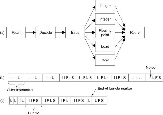
Each machine code word might have two integer
instructions, one floating point instruction, and so forth. Modern designs issue bundles with an
end–of–bundle mark.
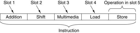
The TriMedia
VLIW Central Processing Unit
The
TriMedia processor was designed by Philips, the Dutch electronics company that
also designed the CD, and CD–ROM (Ref. 4).
It is designed for media–intensive applications, such as image
processing, CD and DVD recorders or players, digital video cameras, digital
television sets, etc. The TriMedia is a
true VLIW processor.
Each
machine language instruction commonly specifies five operations. The machine word is divided into five slots,
one per operation to be issued. Each slot
commands one or more function units; so that some slots are “special purpose”.
Here is
the format of a typical TriMedia machine instruction.
The
TMS3260 implementation runs at 250 MHz.
Since it can issue five operations per clock cycle, it has an effective
maximum rating of 1250 MIPS.
The TriMedia has a byte–oriented memory. It uses memory–mapped I/O, in which each I/O
device is accessed through registers mapped into the memory address space.
The TriMedia
Processors
Here is
a table taken from the Wikipedia article on the history of TriMedia processors.
|
Core |
year 1st silicon |
ISA |
Features |
Cache (I/D) KB |
frequency (worst case) |
introduction
technology |
|
TM1000 |
1997 |
TMA0 |
|
32/16 |
100 MHz |
500 nm |
|
TM1100 |
1998 |
TMA1 |
|
32/16 |
133 MHz |
350 nm |
|
TM1300 |
1999 |
TMA1 |
|
32/16 |
166 MHz |
250 nm |
|
TM3260 |
2002 |
TMA2 |
binary compatible with TM1300 |
64/16 |
250 MHz |
130 nm |
|
TM5250 |
2004 |
TMA3 |
128 KB L2 data cache, allocate on
write miss, hardware prefetching, super pipelined (high speed) |
64/16 |
450 MHz |
130 nm |
|
TM2270 |
2006 |
TMA3 |
96 GPRs (small area) |
32/16 |
290 MHz |
90 nm |
|
TM3270/1 |
2006 |
TMA4 + ASE |
low power |
64/128 64/32 32/16 |
350 MHz |
90 nm |
The
Tanenbaum textbook is based on the TM3260.
Note the successor processors.
1. The
TM5250, operating at 450 MHz. It is more
powerful.
2. The
TM2270 and TM3270, designed to be small and/or low in power consumption.
The two common market pressures are high performance
and low power usage.
The TriMedia
CPU: Details
The CPU
has 128 general purpose registers, each holding a 32–bit number. Two of the registers store constant values:
R0 stores 0 and R1 stores 1. All others
are general purpose and can store integers (8, 16, or 32 bits) or IEEE–754
floating point values.
The
TMS3260 has 12 functional units, a control unit and eleven for doing
arithmetical, logical, and control flow operations. Some of these units respond only to
instructions in specific instruction slots; others can be commanded from any instruction
slot.
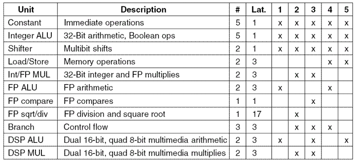
The latency is the number of steps to move a result
through the functional unit.
The last five columns show the placement of commands for each functional unit.
The TriMedia
CPU: Mathematical Units
The
standard arithmetic units use the two’s–complement standard for integer arithmetic,
but the DSP (Digital Signal Processor) units use saturation arithmetic.
In saturation arithmetic, an operation
that produces a result not representable due to overflow saturates at the
maximum value rather than generating an exception.
For
example, the range of numbers representable by 8–bit unsigned integer
arithmetic is
0 through 255 inclusive. In saturation
arithmetic, 180 + 180 = 255, the maximum value.
With two
minor exceptions, all operations in the TriMedia are predicated.
In a
predicated instruction, each operation specifies a register that is to be
tested before the operation is executed.
The low–order bit of the register is examined.
0. If
that bit is 0, the operation is skipped.
1. If
that bit is 1, the operation is executed.
IF R2 IADD R4, R5 ® R8 //
Add R4 to R5 and place result into R8.
//
But only if bit 0 of R2 is a 1; otherwise do nothing.
Using R1
as the predicate register makes it unconditional as R1 º 1.
Using R0 as a predicate register makes is a no–op as
R0 º 0.
Heterogeneous
Processor Example: The DVD Player
The
computer controlling the DVD player has a number of very different functions.
Each of these is assigned to a specialized processor.
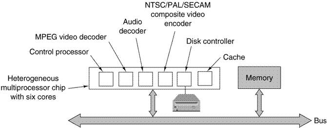
This
design uses multiple cores on a single large chip. A core
is a large circuit, such as a CPU, I/O controller, or cache, that can be placed
on a chip in a modular way. Some modern
processors are dual–core in that
they have two cores, each being a full CPU.
This design might be called “heterogeneous multi–core”.
Each of the closely–coupled cores has a dedicated function related to
the format of the data it must process.
This design was found to be more economical than a single
general–purpose CPU.
Computers
From “Piece Parts”
We now
face the issue of how to design computers and their major components.
Main
components, such as the CPU, will continue to be designed from basic gates in
the traditional way for some time. Here
the advantage in performance gained from a single integrated design justifies
the cost and effort involved.
We now
have another attractive option for the design of computing machines. This one is made attractive by the
availability of a variety of cores, each with a dedicated function. This collection of cores can be considered
essentially as a set of libraries of functions, only that these functions are
implemented in hardware.
IBM has produced a design, called CoreConnect, which
is an architecture for connecting cores on a single–chip heterogeneous
multiprocessor. Here is an example.
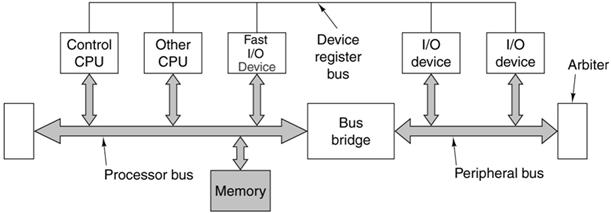
Note the
two busses; one is faster than the other.
The Global
Internet and the Network Interface Card (NIC)
You may
think that your computer is connected to the Internet, but it is not. The computer is connected to a NIC; it is
that NIC that is connected to the Internet.
The NIC
is a dedicated I/O coprocessor, which communicates with the computer’s CPU via
interrupts and DMA (Direct Memory Access).
Except when the NIC is operated in “promiscuous mode” (for network
snooping), it filters all packets by MAC address.
The
standard of transmission that we shall discuss is called “Ethernet”. Packets in this
protocol possess two 48–bit MAC (Media Access Control) addresses, one for the
source and one for the destination NIC (Interface Card).
Here is
the format of an Ethernet packet containing an IP packet.

The
Ethernet header contains the two MAC addresses.
Each NIC has a unique MAC address assigned to it under a protocol
administered by the IEEE. In normal use,
the NIC will recognize messages sent to its MAC address and pass only those to
the CPU.
The NIC
(Network Processor)
The NIC
is programmable device that can handle incoming and outgoing packets
at the full network speed. It is plugged
into a standard slot in the computer motherboard.
One or
more network lines connect to the board and are routed to the network
processor.
Most setups have only a single network line attached, but computers used as
switches, routers, and the like must have at least two network lines attached.
Here is a diagram of a typical network processor,
using a PCI slot on the motherboard.
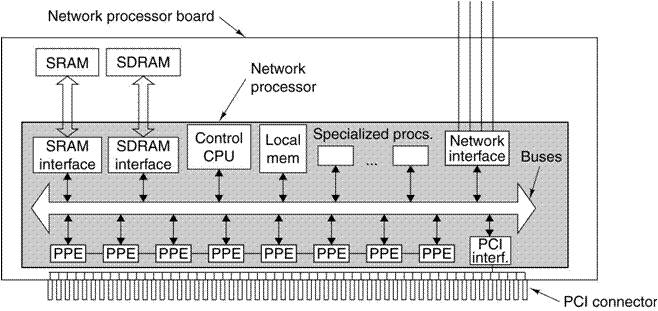
Note the multiple PPE (Packet Processing
Engines). Each is a specialized core
with a dedicated task; the set forms a packet processing pipeline.
The Nexperia
Media Processor
Ordinary
general–purpose processors are not especially good at the massively parallel
computations required to process high–resolution audio and video streams.
The
Nexperia is a single–chip heterogeneous multiprocessor designed by Philips,
using its TriMedia chip. It comprises a
heterogeneous collection of cores, each with a dedicated function for which it
has been optimized. Here is the PNX
1500.
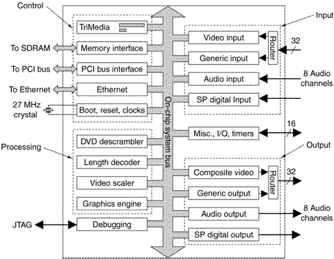
More on the
Nexperia
The
Nexperia is designed for use either as a coprocessor in a PC or as a
stand–alone main processor in an appliance such as a DVD player, digital TV
set, video camera, etc.
Other
than the SRAM and SDRAM internal to the TriMedia processor, the Nexperia
contains no main memory on the chip. The
PNX 1500 implementation has an interface to external memory, allowing for 8 to
256 MB of DDR SDRAM.
The
width of the memory interface is 32 bits (4 bytes). This allows the DDR memory to transfer 8
bytes per clock pulse; at 200 MHz the data rate is 1.6 GB/second.
The
processing units (DVD Descrambler, Length Decoder, Video Scaler, and Graphics
Engine) perform computations related to the display of encrypted video as found
on a commercial DVD.
Note
that there is a core dedicated to debugging.
It follows the JTAG (Joint Test Action Group) protocols, defined in IEEE
Standard 1149.1 – the industry standard.
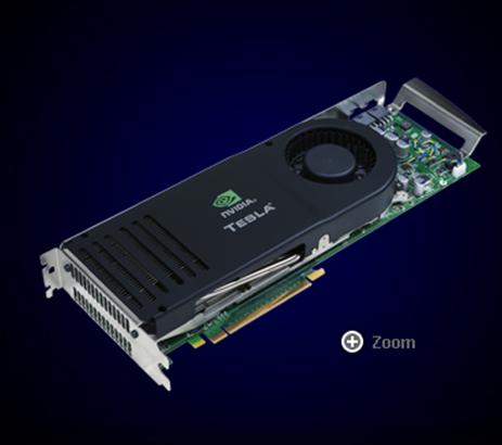
A High–End
Graphics Coprocessor
Here are
some data on the NVIDIA GeForce 9 Series (9800 GX2 and 9800 GTX). The table is taken from the web site (Ref.
6).
|
|
Core Clock (MHz) |
Shader Clock (MHz) |
Memory Clock (MHz) |
Memory Amount |
Memory Interface |
Memory Bandwidth
(GB/sec) |
Texture Fill Rate
(billion/sec) |
|
9800 GX2 |
600 |
1500 |
1000 |
1 GB |
512-bit |
128 |
76.8 |
|
9800 GTX |
675 |
1688 |
1100 |
512MB GDDR3 |
256-bit |
70.4 |
43.2 |
|
9600 GT |
650 |
1625 |
900 |
512MB |
256-bit |
57.6 |
20.8 |
The 9800
GX2 is a multi–core design with 256 stream processors. It has a 512 bit
(64 byte) memory interface operating at a peak rate of 128 gigabytes per
second.
This
produces video at resolutions up to 2560 by 1600 pixels.
The cost
of the 9800 GX2 is $520 (Ref. 6, 4/16/2008).
A High–End
Audio Processor
Here are
some data on the SoundBlaster XtremeGamer Fatal1ty Pro Series.
It is an audio attached coprocessor for use with a PC.
24–bit
Analog to Digital conversion 96 kHz
sample rate
24–bit
Digital to Analog conversion 96 kHz
rate to either 7.1 audio or standard stereo.
64 MB
random access memory, called “XRAM”.
Signal–to–Noise
Ratio 109 dB for stereo output
Total
Harmonic Distortion 0.004%
Frequency
Response 10 Hz to 46 kHz (–3
dB points)
Note: These audio specifications would be considered
extremely good
for a high–priced audio system
for home use.
The cost
of this coprocessor is $150.00 (Ref. 7, 4/16/2008)
Cryptographic
Coprocessors
Suppose
two workstations that are to communicate over the public Internet in a secure
mode. The provision of industrial–grade
cryptography is very compute intensive.
Again,
cryptography does not lend itself to solution by a general–purpose
processor. For this reason, and also to
offload the computational burden from the primary CPU, many secure
communication systems use attached cryptographic processors.
Here are
some data on a cryptographic processor marketed by IBM (Ref. 8). The product described is the IBM PCI
Cryptographic Coprocessor.
The
coprocessor provides DES, triple–DES, RSA, and DSA encryption, all national
standards. The hardware is certified
under FIPS PUB 140–1 (Security Requirements for Cryptographic Modules), at
level 3. The mainframe version is
certified to level 4.
The
coprocessor has a “tamper–sensing and tamper–responding environment” to limit
and report unauthorized access to the processor itself.
The
price of this unit was not quoted.
Game Engines
as Supercomputers
It may
surprise students to learn that many of these high–end graphics processors are
actually export controlled as munitions.
In this case, the control is due to the possibility of using these
processors as high–performance computers.
In the
next slide, we present a high–end graphics coprocessor that can be viewed as a
vector processor. It is capable of a
sustained rate of 4,300 Megaflops.
Compare
this to the CRAY–1 supercomputer of 1976, with a sustained computing
rate of 136 Megaflops and a peak rate of 250 Megaflops. This is about 3.2% of the performance of the
current graphics coprocessor at about 500 times the cost.
The Cray
Y–MP was a supercomputer sold by Cray Research beginning in 1988.
Its peak performance was 2.66 Gigaflops (8 processors at 333 Megaflops each).
Its memory comprised 128, 256, or 512 MB of static RAM.
The
earliest supercomputer that could outperform the current graphics processor
seems to have been the Cray T3E–1200E™, a MPP (Massively Parallel Processor) introduced
in 1995 (Ref. 9). In 1998, a joint
scientific team from Oak Ridge National Lab, the University of Bristol (UK) and
others ran a simulation related to controlled fusion at a sustained rate of
1.02 Teraflops (1020 Gigaflops).
The next
slide shows this current graphics coprocessor.
The NVIDIA
Tesla C870
Data
here are from the NVIDIA web site (Ref. 6).
I quote from their advertising copy.
 The C870 processor is a “massively multi–threaded
processor architecture that is ideal for high performance computing (HPC)
applications”.
The C870 processor is a “massively multi–threaded
processor architecture that is ideal for high performance computing (HPC)
applications”.
This has
128 processor cores, each operating at 1.35 GHz. It supports the IEEE–754 single–precision
standard, and operates at a sustained rate of 430 gigaflops (512 GFlops peak).
The typical
power usage is 120 watts. Note the
dedicated fan for cooling.
The
price is $1300, with an introductory offer at $650.
The
processor has 1.5 gigabytes of DDR SDRAM, operating at 800 MHz. The data bus to memory is 384 bits (48 bytes)
wide, so that the maximum sustained data rate is
48 2 800 106 = 76.8 Gigabytes per second.
References
In this lecture, material from one or more of the
following references has been used.
1. Computer
Organization and Design, David A. Patterson & John L. Hennessy,
Morgan Kaufmann, (3rd
Edition, Revised Printing) 2007, (The course textbook)
ISBN 978 – 0 – 12 – 370606 – 5.
2. Computer
Architecture: A Quantitative Approach, John L. Hennessy and
David A. Patterson, Morgan
Kauffman, 1990. There is a later
edition.
ISBN 1 – 55860 – 069 – 8.
3. High–Performance
Computer Architecture, Harold S. Stone,
Addison–Wesley (Third Edition),
1993. ISBN 0 – 201 – 52688 – 3.
4. Structured
Computer Organization, Andrew S. Tanenbaum,
Pearson/Prentice–Hall (Fifth
Edition), 2006. ISBN 0 – 13 – 148521 – 0
5. http://en.wikipedia.org/wiki/TriMedia
7. http://www.soundblaster.com