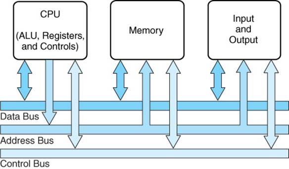
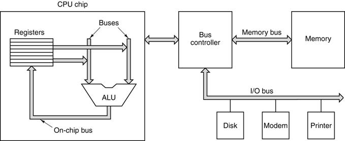
The CPU
Interacts Via the System Bus
The System Bus
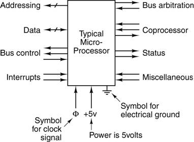
allows the CPU to interact with the rest of the system. Each of the logical pinouts on the previous
figure is connected to a line in the system bus.
Ground lines on the bus have two purposes
1. To complete the electrical circuits
2. To minimize cross–talk between the signal lines.
Here is a small bus with three data lines (D2,
D1, D0), two address lines (A1, A0),
a system clock (F) and a voltage line (+ V).
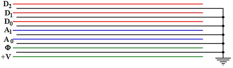
In our considerations, we generally ignore the
multiple grounds, and the power lines.
Notations
Used for a Bus
Here is the way that we would commonly represent the
small bus shown above.
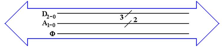
The big “double arrow” notation indicates a bus of a number of
different signals.
Our author calls this a “fat arrow”.
Lines with similar function are grouped together. Their count is denoted with the
“diagonal slash” notation.
From top to bottom, we have
1. Three
data lines D2,
D1, and D0
2. Two address lines A1 and A0
3. The clock signal for the bus F
Power and ground lines usually are not shown in this
diagram.
Computer
Systems Have Multiple Busses
Early computers had only a single bus, but this could
not handle the data rates.
Modern computers have at least four types of busses
1. A video bus to the display unit
2. A memory bus to connect the CPU to memory, which
is often SDRAM.
3. An I/O bus to connect the CPU to Input/Output
devices.
4. Busses internal to the CPU, which generally
has at least three busses.
Often the proliferation of busses is for backward
compatibility with older devices.
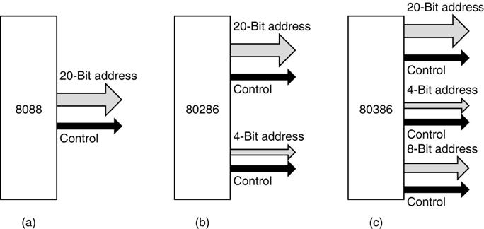
Backward
Compatibility in PC Busses
Here is a figure that shows how the PC bus grew from a
20–bit address through
a 24–bit address to a 32–bit address while retaining backward compatibility.
Backward
Compatibility in PC Busses (Part 2)
Here is a picture of the PC/AT bus, showing how the
original configuration was kept and augmented, rather than totally revised.
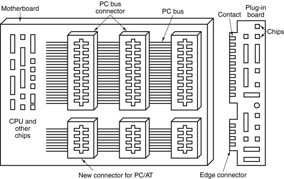
Note that the top slots can be used by the older 8088
cards, which do not have the
“extra long” edge connectors.
Notation for
Bus Signal Levels
The system clock is represented as a trapezoidal wave
to emphasize the fact that it does not change instantaneously.
Here is a typical depiction. Others may be seen, but this is what our
author uses.
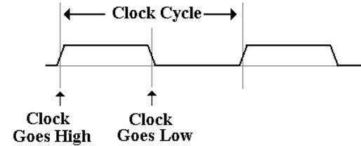
Single control signals are depicted in a similar
fashion, except (of course) that they
may not vary in “lock step” with the bus clock.
Notation for
Multiple Signals
A single control signal is either low or high (0 volts
or 5 volts).
A collection, such as 32 address lines or 16 data
lines cannot be represented with such a simple diagram. For each of address and data, we have two
important states
address or data is valid
address or data is not valid
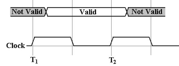
For example, consider the address lines on the
bus. Imagine a 32–bit address.
At some time after T1, the CPU asserts an
address on the address lines. This means
that each of the 32 address lines is given a value.
When the CPU has asserted the address, it is valid
until the CPU ceases assertion.
Reading Bus
Timing Diagrams
Sometimes,
we need to depict signals on a typical bus.
Here we are looking at a
synchronous bus, of the type used
for connecting memory.
This
figure, taken from the textbook, shows the timings on a typical bus.
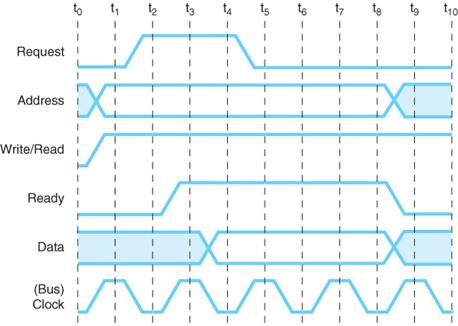
Note
the form used for the Address Signals: between t0 and t1
they change value.
According to the figure, the address signals remain valid from t1
through the end of t7.
Read Timing
on a Synchronous Bus
The bus protocol calls for certain timings to be met.
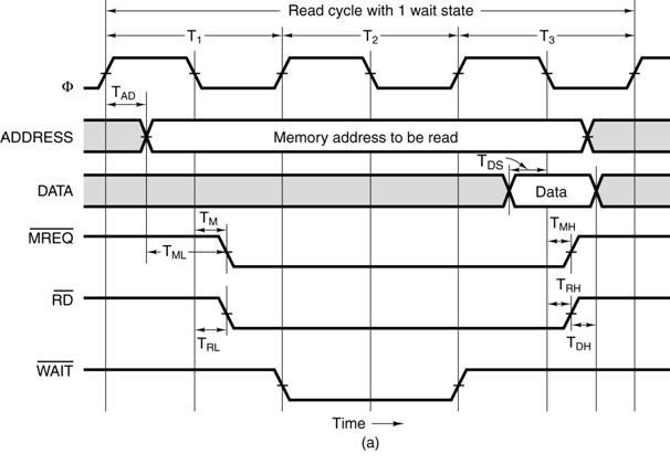
TAD the
maximum allowed delay for asserting the address after the clock pulse
TML the minimum time that the
address is stable before the MREQ is asserted.
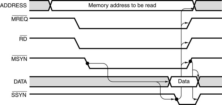
Read
Sequences on an Asynchronous Bus
Here the focus is on the protocol by which the two
devices interact.
This is also called the “handshake”.
The bus master asserts MSYN and the bus slave responds with SSYN when done.
Attaching an
I/O Device to a Bus
This
figure shows a DMA Controller for a disk attached to a bus.
It is only slightly more complex than a standard controller.
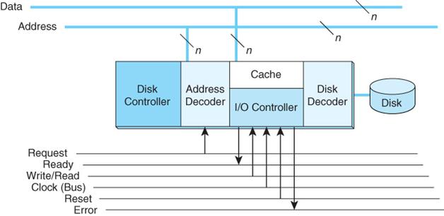
Each
I/O Controller has a range of addresses to which it will respond.
Specifically,
the device has a number of registers, each at a unique address.
When
the device recognizes its address, it will respond to I/O commands sent on the
command bus.
Bus
Arbitration
A number of I/O devices are usually connected to a
bus.
Each I/O device can generate an Interrupt, called “INT”
when it needs service.
The CPU will reply with an acknowledgement,
called “ACK”.
The handling by the CPU is simple. There are two signals only
INT some
device has raised an interrupt
ACK the
CPU is ready to handle that interrupt.
We need an arbitrator to take the ACK and pass it to
the correct device.
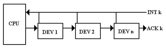
The common architecture is to use a “daisy chain”, in which the ACK is
passed
from device to device until it reaches the device that raised the interrupt.
Details of
the Device Interface
Each device has an Interrupt Flip–Flop that is set
when the device raises the interrupt.
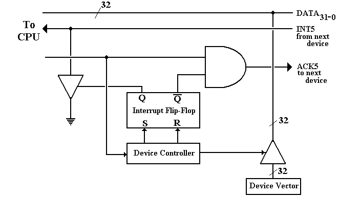
Note that the interrupt line is grounded out as a
signal to the CPU.
The ACK comes from the left of the figure and is
trapped by the AND gate.
The device identifies itself by a “vector”, a pointer
to the address of the device
controller that will handle the I/O.