PCI Express
This lecture is
based on the Peripheral Component Interconnect Express,
which is a standard for computer expansion cards.
More
specifically, this is a standard for the communication link by which a
PCIe device communicates with the CPU.
According to
Wikipedia, PCIe 3.0 (August 2007) is the latest standard.
The PCIe
standard is an outgrowth of the original PCI standard, but is not
compatible with PCI at the hardware level.
The PCIe
standard is based on a new protocol for electrical signaling.
This protocol is built on the concept of a lane, which we must define.
Here are some
capacity quotes from Wikipedia
Per Lane 16–Lane Slot
Version 1 250 MB/s 4 GB/s
Version 2 500 MB/s 8 GB/s
Version 3 1 GB/s 16 GB/s
What is a Lane?
A lane is pair
of point–to–point serial links.
It is a
full–duplex link, able to communicate in two directions simultaneously.
Each of the serial links in the pair handles one of the two directions.
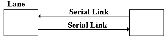
By definition, a
serial link transmits one bit at a
time.
By extension, a lane may transmit two bits at any one
time,
one bit in each direction.
One may view a parallel link, transmitting multiple
bits in one direction
at any given time, as a collection of serial links.
The only
difference is that a parallel link must provide for synchronization
of the bits sent by the individual links.
Data Transmission Codes
The PCIe
standard is byte oriented, in that it should be viewed logically
as a full–duplex byte stream. What is
actually transmitted?
The association
of bits (transmitted or received) with bytes is handled at the
Data Link layer. Suppose a byte is to be
transmitted serially.
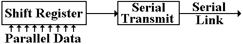
The conversion
from byte data to bit–oriented data for serial transmission
is done by a shift register. The
register takes in eight bits at a time and
shifts out one bit at a time.
The bits, as
shifted out, are still represented in standard logic levels.
The serial
transmit unit takes the standard logic levels as input, and
converts them to voltage levels appropriate for serial transmission.
Three Possible Transmission Codes
The serial
transmit unit sends data by asserting a voltage on the serial link.
On simple method
would be as follows.
To transmit a
logic 1, assert +5 volts on the transmission line.
To transmit a
logic 0, assert 0 volts on the transmission line.
This simple
method has so many difficulties in practice that it cannot be used.
Two of the most obvious are transmission of power and lack of data framing.
Standard methods
for link management use codes that avoid these problems.
Two of the more common methods used are NRZ and NRZI.
Non–Return–to–Zero coding transmits by asserting
the following voltages:
For a logic
1, it asserts a positive voltage (3.0 – 5.0 volts) on the link.
For a logic 0, it asserts a
negative voltage (–3.0 to –5.0 volts).
Non–Return–to–Zero–Invert is a
modification of NRZ, using the same
voltage levels.
The Problem of Noise
One problem with
these serial links is that they function as antennas.
They will pick up any stray electromagnetic radiation if in the radio range.
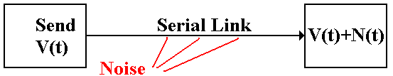
In other words,
the signal received at the destination might not be what
was actually transmitted. It might be
the original signal, corrupted by noise.
The solution to
the problem of noise is based on the observation that two links
placed in close proximity will receive noise signals that are almost identical.
To make use of
this observation, we use differential
transmitters to send the
signals and differential receivers
to reconstruct the signals.
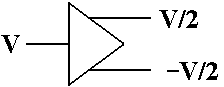
Differential Transmitters and
Receivers
In differential
transmission, rather than asserting a voltage on a single output
line, the transmitter asserts two voltages: +V/2 and –V/2.
A +6 volt signal
would be asserted as two: +3 volts and –3 volts.
A –8 volt signal
would be asserted as two: –4 volts and +4 volts.
Here is a
standard diagram of a differential transmitter.
The standard
differential receiver is an analog subtractor.
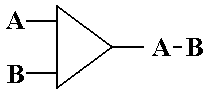
For
a 6 volt transmitted signal, we have A = 3, B = –3; A – B = 3 – (–3) = 6.
Noise in a Differential Link
We now assume
that the lines used to transmit the differential signals are
physically close together, so that each line is subject to the same noise
signal.
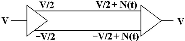
Here the
received signal is the difference of the two voltages input to
the differential receiver.
The value
received is V/2 – (–V/2) = V, the desired value.
Ground Offsets in Standard Links
All voltages are
measured relative to a standard value, called “ground”.
Here is the
complete version of the simple circuit that we want to implement.
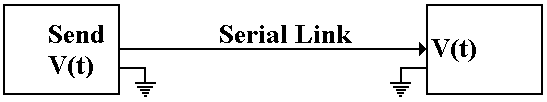
Basically, there
is an assumed second connection between the two
devices. This second connection fixes
the zero level for the voltage.
There is no
necessity for the two devices to have the same ground. Suppose
that the ground for the receiver is offset from the ground of the transmitter.
The signal sent
out as +V(t) will be received as V(t) – VO.
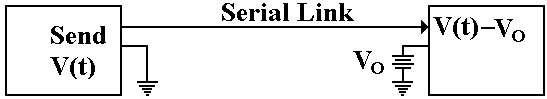
Ground Offsets in Differential
Links
Here again, the
subtractor in the differential receiver handles this problem.
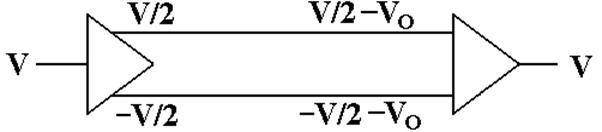
The signal
originates as a given voltage, which can be positive, negative, or 0.
The signal is
transmitted as the pair (+V/2, –V/2).
Due to the
ground offset for the receiver, the signal is taken in as
(+V/2 – VO, –V/2 – VO).
The signal is interpreted as
(+V/2 – VO) – (–V/2 – VO) = +V/2 – VO + V/2 +
VO = V.
The differential
link will correct for both ground offset and line noise
at the same time.
References
1. Wikipedia http://en.wikipedia.org/wiki/PCI_Express
2. Wikipedia http://en.wikipedia.org/wiki/File:Differential_Signaling.png
3. Web Site http://www.interfacebus.com/Design_Connector_RS422.html
4. Wikipedia http://en.wikipedia.org/wiki/RS-422