The
Microprogrammed Control Unit
Up to this point, we have studied:
1. The microoperation sequence associated with
each assembly language instruction
2. The control signals associated with those
microoperations.
3. The use of combinational logic in the form of
a signal generation tree
to generate these control
signals.
We now consider another option for generating the
control signals.
This is the microprogramming option, in which
representations of the control signals
are stored in a micro–memory and read into a mMBR (micro–memory buffer register) from whence they
are issued.
Consider the control signal PC ® B1. When this
is asserted, the contents of the Program Counter are copied onto bus B1. The method of generating this signal has no
effect on the action it takes.
We have two options for generating each control
signal:
Hardwired: The signal is output from an
AND gate
Microprogrammed: The signal is output from a D flip–flop.
Survey of
Bus Usage and Other Control Signals
In order to structure the micro–memory properly, we
must tabulate the control signals used and arrange them by use: bus transfer,
ALU operation, memory operation, etc.
|
Option |
Bus 1 |
Bus 2 |
Bus 3 |
ALU |
Other |
|
0 |
|
|
|
|
|
|
1 |
PC ® B1 |
1 ® B2 |
B3 ®PC |
tra1 |
L / R’ |
|
2 |
MAR ® B1 |
– 1 ® B2 |
B3 ® MAR |
tra2 |
A |
|
3 |
R ® B1 |
R ® B2 |
B3 ® R |
shift |
C |
|
4 |
IR ® B1 |
MBR ® B2 |
B3 ® IR |
not |
READ |
|
5 |
SP ® B1 |
IOD ® B2 |
B3 ® SP |
add |
WRITE |
|
6 |
|
|
B3 ® MBR |
sub |
extend |
|
7 |
|
|
B3 ® IOD |
and |
0 ® RUN |
|
8 |
|
|
B3 ® IOA |
or |
|
|
9 |
|
|
|
xor |
|
Note
the important option 0.
We must have the following options: Place nothing on bus B1, leaving it
undefined.
Place
nothing on bus B2, leaving it undefined.
Do
not transfer bus B3 to any destination register.
The
ALU is not active.
Microprogramming
Example
In a microprogrammed control unit, binary encodings of
the microoperations
are stored in a micro–memory, one microoperation per micro–memory word.
The control signals are generated when the
micro–memory word is read
into a micro–memory buffer register (mMBR).
The structure of micro–memory is independent of that
for the main memory.
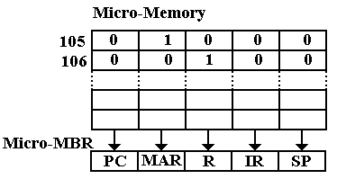
Consider a section of micro–memory associated with bus
B1.

The microoperation at address 105 corresponds to MAR ® B1.
The microoperation at address 106 corresponds to R ® B1.
Horizontal
and Vertical Microcoding
In horizontal
microcoding, each control signal is represented by a single bit
in each micro–memory word. The signal is
asserted if and only if that bit is 1.
Horizontal microcoding demands a “wide micro–memory”,
with each word having
a large number of bits. In earlier
designs this was a problem.
In horizontal microcoding, there would be five bits in
each micro–memory word
corresponding to actions on bus B1; one for each possible data source.
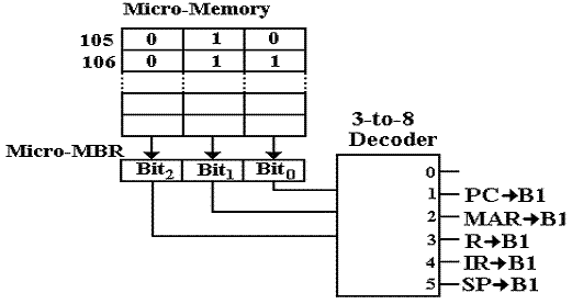
In vertical microcoding, each control signal is
assigned a binary code, and
it is that binary code that is stored in the micro–memory word.
There are six options for bus B1: five data sources
and the undefined option.
This requires three binary bits to encode.
Here are the encodings for B1.
|
Code |
Signal |
|
000 |
|
|
001 |
PC ® B1 |
|
010 |
MAR ® B1 |
|
011 |
R ® B1 |
|
100 |
IR ® B1 |
|
101 |
SP ® B1 |
Advantages
of Vertical Microcoding
There are a number of advantages to the use of
vertical microcoding,
not all of which are important today.
One advantage is that it allows a “narrower micro–memory”,
fewer bits per word in the micro–memory.
The
major advantage is that it prevents the assertion of two or more
data sources on a given bus or two or more simultaneous ALU operations.
For bus B1, each data source is assigned a binary
code.
At most one data source can be placed on this bus for any microoperation.
For the ALU, each action is assigned a binary code.
At most one ALU action can be invoked by any microoperation.
Bus B1:
Horizontal vs. Vertical Microcoding
Here is the horizontal microcode design for 105: MAR ® B1, 106: R ® B1.
Here is the vertical microcode design for 105: MAR ® B1, 106: R ® B1.
Structure of
the Boz–5 Microcode
The Boz–5 microprogrammed control unit will be
implemented using a mix of vertical and horizontal microcode.
The fields that specify the source register for busses
B1 and B2, the destination register for bus B3 and the ALU function will be
encoded to disallow two or more functions.
Thus vertical microcoding is used for these fields.
The seven control signals, labeled as “Other” and
associated with a field of that name,
can each be issued simultaneously with the others. For these bits, no encoding is necessary and
horizontal microcoding is used.
The following table shows the allocation of bits in
the microcode to these fields.
|
Field |
Bits Required |
Bits Allocated |
|
B1 |
3 |
4 |
|
B2 |
3 |
4 |
|
B3 |
4 |
4 |
|
ALU |
4 |
4 |
|
Other |
7 |
8 |
The
reason for allocating multiples of 4 bits to each field is purely for teaching
purposes.
In the microcode, each field will be represented by
one or two hexadecimal digits.
The
Micro–Opcode
At this point, we use prior experience, including both
standard programming and that gained in design of the hardwired control unit,
to postulate the necessity for opcodes in the microprogram.
Some microinstructions will cause control signals to
be emitted.
However, our previous experience leads us to expect
that we shall need certain specific microinstructions to sequence the
microprogram.
These specific instructions might be compared to the
conditional branch instruction found in the assembly language and reflected in
control structures of higher level languages.
We might ask about the idea of
“micro–subroutines”. While these might
appear to be a good solution, they waste too much time and are overly complex.
Here are options for handling the Defer state. Recall that only four instructions use it. In microcode Defer needs only 3
microinstructions; a micro–return brings that up to 4.
The In–Line microcode option requires 12
microinstructions, 3 for each possible use.
The “micro–subroutine” requires expansion of Defer to
4 microinstructions, but requires only one additional microoperation per call:
4·1 + 4 = 8.
For
this reason, the design avoids micro–subroutines.
The
Microinstruction Format at This Point
While we do not yet know the required number of
micro–opcodes, we suspect that it is probably going to be small.
To facilitate teaching this microarchitecture, the
design calls for a 4–bit micro–opcode.
Far fewer will actually be needed.
At this point, the structure of the micro–word has
evolved to that shown in the figure.
|
Micro–Op |
B1 |
B2 |
B3 |
ALU |
Other |
|
4 bits |
4 bits |
4 bits |
4 bits |
4 bits |
8 bits |
We
shall find it convenient to split the field called “Other” into two distinct
4–bit fields, tentatively called “M1” and “M2”.
Field M1 will hold the shift control signals.
|
Micro–Op |
B1 |
B2 |
B3 |
ALU |
M1 |
M2 |
|
4 bits |
4 bits |
4 bits |
4 bits |
4 bits |
4 bits |
4 bits |
Now each
field can be specified by a single hexadecimal digit.
This is done for teaching purposes only.
What else do we need?
The requirements come from the Fetch and Defer cycles that appear
explicitly in the hardwired design and implicitly here.
Fetch
Reconsidered
Recall the microoperations and control signals
associated with the Fetch phase.
F, T0: PC ® B1, tra1, B3 ® MAR, READ. // MAR ¬ (PC)
F, T1: PC ® B1, 1 ® B2, add, B3 ® PC. // PC ¬ (PC) + 1
F, T2: MBR ® B2, tra2, B3 ® IR. // IR ¬ (MBR)
F, T3: Do
something that is specific to the assembly language instruction
This
sequence maps almost effortlessly into a sequence of four microinstructions in
the microprogrammed control unit, except that the latter needs an explicit
dispatch.
F, T0: PC ® B1, tra1, B3 ® MAR, READ. // MAR ¬ (PC)
F, T1: PC ® B1, 1 ® B2, add, B3 ® PC. // PC ¬ (PC) + 1
F, T2: MBR ® B2, tra2, B3 ® IR. // IR ¬ (MBR)
F, T3: Jump to
the microprogram that is specific to this assembly language instruction.
First Try at
the Microcode Structure
We start with a preliminary design and evolve it as
necessary.
At this point in the design, the microcode will be
written as the equivalent control signals.
Assume a micro–memory of 256 words, with addresses
0x00 through 0xFF.
Any addresses used will need to be 8–bit addresses (two hexadecimal digits).
We shall arbitrarily specify that micro–opcode 0 is
reserved for emitting control signals.
We shall use the micro–opcode 1 for the dispatch based
on the op–code found in the machine language instruction in the Instruction
Register (IR).
Address Micro–Op Control
Signals Comment
0x20 0 PC ® B1, tra1, B3 ® MAR, READ. //
F, T0
0x21 0 PC ® B1, 1 ® B2, add, B3 ® PC. // F,
T1
0x22 0 MBR ® B2, tra2, B3 ® IR. // F, T2
0x23 1 No control signals. // F, T3
Dispatch
based on op–code.
First Trial
Implementation
Let’s look at the consequences of this first try.
Assume that the assembly language instruction AND is
being executed, and
that the execute microcode for that instruction is at address 0x80.
The structure to this point will play out as follows.
Address Micro–Op Control
Signals Comment
0x20 0 PC ® B1, tra1, B3 ® MAR, READ. //
F, T0
0x21 0 PC ® B1, 1 ® B2, add, B3 ® PC. // F,
T1
0x22 0 MBR ® B2, tra2, B3 ® IR. // F, T2
0x23 1 No control signals. // F, T3
Dispatch
based on op–code.
0x80 0 R ® B1, R ® B2, and,
B3 ® R
0x81 2 No control signals.
Go
to address 0x20 for the next Fetch.
This design has two major problems:
1. It
allocates two clock pulses to execute the instruction.
2. It
requires some sort of dispatch table to find the microprogram address.
Executing in
One Clock Pulse
Note here that our main concern is time efficiency of
the microcode execution.
A faster microcode interpretation of the assembly
language
yields a faster execution of that assembly language; thus a faster computer.
We are not at all worried about efficient use of
micro–memory as it is so small.
Any reasonable design will leave much of a micro–memory unused.
Observations
1. Many of the assembly language instructions
require only one clock pulse
for the execution itself.
2. Encoding the address of the next
microinstruction into each micro–word
can remove the additional
instruction to execute a branch.
This design modifies the structure of each micro–word
to be as follows.
|
Micro–Op |
B1 |
B2 |
B3 |
ALU |
M1 |
M2 |
Next Address |
|
4 bits |
4 bits |
4 bits |
4 bits |
4 bits |
4 bits |
4 bits |
8 bits |
Second Trial
Implementation
Let’s look at the consequences of this second try.
Assume that the assembly language instruction AND is
being executed, and
that the execute microcode for that instruction is at address 0x80.
The structure to this point will play out as follows.
Address Micro–Op Control
Signals Next
Address
0x20 0 PC ® B1, tra1, B3 ® MAR, READ. 0x21
0x21 0 PC ® B1, 1 ® B2, add, B3 ® PC. 0x22
0x22 0 MBR ® B2, tra2, B3 ® IR. 0x23
0x23 1 No control signals. Not used
Dispatch
based on op–code.
0x80 0 R ® B1, R ® B2, and,
B3 ® R 0x20
We have solved
the problem associated with the extra microinstruction for the
explicit jump to the beginning of the Fetch sequence.
It turns out that we have also solved the “dispatch
table” problem; that is, the
association of an address in micro–memory with the execution of each opcode.
Solution of
the Dispatch Problem
At present, microinstructions in addresses 0x20
through 0x22 correspond to (F, T0) through (F, T2) in determining what assembly
language instruction is being executed.
The microinstruction at 0x23 is a dispatch
instruction; it jumps to the code appropriate to execute that assembly language
instruction.
With the explicit encoding of the next address in
micro–memory, we have a very simple dispatch mechanism; just place the execute
for a given op–code at that address.
In the ISA, we use opcodes 0x00 through 0x1F (0
through 31).
We allocate micro–memory addresses 0x00 through 0x1F
to the first step in executing each instruction. This will correspond to (F, T3).
For the logical AND instruction (Opcode = 10111 =
0x17) we have this situation.
Address 0x17 contains
the control signals that were associated with (F, T3)
Address 0x20 contains
the control signals that were associated with (F, T0)
Address 0x21 contains
the control signals that were associated with (F, T1)
Address 0x22 contains
the control signals that were associated with (F, T2)
Address 0x23 contains
the dispatch, here equivalent to a Jump to 0x17.
Example:
Dispatching the AND
Assembly Language Instruction
Address Micro–Op Control
Signals Next
Address
0x17 0 R ® B1, R ® B2, and,
B3 ® R 0x20
0x20 0 PC ® B1, tra1, B3 ® MAR, READ. 0x21
0x21 0 PC ® B1, 1 ® B2, add, B3 ® PC. 0x22
0x22 0 MBR ® B2, tra2, B3 ® IR. 0x23
0x23 1 No control signals. Not used
Jump
to address 0x17
What about the unused opcodes in the ISA?
As an example, the opcode 00100 (0x04) has no assembly
language instruction
associated with it. It should just do
nothing and return to Fetch. That is
what it does.
Address Micro–Op Control
Signals Next
Address
0x04 0 None issued 0x20
What About
the Execute Phase?
This structure works well for instructions that can
execute in one clock pulse.
What about those that require two or more clock pulses
to execute?
It is for these instructions that we developed the execute phase in the hardwired
design.
We use the explicit next address to solve this
problem.
Consider the GET instruction, used for input from an
I/O device.
We had written the following sequence.
GET Op-Code = 01000 (Hexadecimal 0x08)
F, T0: PC ® B1, tra1, B3 ® MAR, READ. //
MAR ¬ (PC)
F, T1: PC
® B1, 1 ® B2, add, B3 ® PC. // PC ¬ (PC) + 1
F, T2: MBR
® B2, tra2, B3 ® IR. // IR ¬ (MBR)
F, T3: WAIT.
E, T0: IR
® B1, tra1, B3 ® IOA. // Send out the I/O address
E, T1: WAIT.
E, T2: IOD
® B2, tra2, B3 ® R. // Get the
results.
E, T3: WAIT.
What
goes at micro–memory location 0x08 and how do we handle the execution?
Microprogramming
the GET Assembly Language Operation
We get the desired microprogram structure by first
omitting any major state references.
T0: PC ® B1, tra1, B3 ® MAR, READ. //
Address = 0x20
T1: PC
® B1, 1 ® B2, add, B3 ® PC. // Address
= 0x21
T2: MBR
® B2, tra2, B3 ® IR. //
Address = 0x22
T3: IR
® B1, tra1, B3 ® IOA. // Address
= 0x08
T4: IOD
® B2, tra2, B3 ® R. // Where?
We now just start filling the micro–memory addresses
that follow the common fetch.
Address Micro–Op Control
Signals Next
Address
0x08 0 IR ® B1, tra1, B3 ® IOA 0x24
0x20 0 PC ® B1, tra1, B3 ® MAR, READ. 0x21
0x21 0 PC ® B1, 1 ® B2, add, B3 ® PC. 0x22
0x22 0 MBR ® B2, tra2, B3 ® IR. 0x23
0x23 1 No control signals. Jump to 0x08 Not
used
0x24 0 IOD ® B2, tra2,
B3 ® R 0x20
This explicit “next address” structure does solve a
lot of problems, but not all of them.
What About
the Defer Phase?
Consider the fetch sequence for LDR (Load Register)
completely written out
with explicit reference to what the major state register does.
LDR Op-Code
= 01100 (Hexadecimal 0x0C)
F, T0: PC
® B1, tra1, B3 ® MAR, READ. // MAR ¬ (PC)
F, T1: PC
® B1, 1 ® B2, add, B3 ® PC. // PC ¬ (PC) + 1
F, T2: MBR
® B2, tra2, B3 ® IR. // IR ¬ (MBR)
F, T3: IR
® B1, R ® B2, add, B3 ® MAR. // Do the indexing.
Here the
major state register takes control.
1) If the I–bit (bit 26) is 1, then the Defer
state is entered.
2) If
the I–bit is 0, then the E state is entered.
The
current microprogram solution calls for the following.
Address Micro–Op Control
Signals Next
Address
0x0C 0 IR ® B1, R ® B2, add,
B3 ® MAR Depends on I26.
Suddenly we need two “next instruction” addresses; one
for D = 0 and another for D = 1.
Selection
Problem for the Next Address
This need for encoding two possible addresses leads to
the final
format of the microinstruction.
|
Micro–Op |
B1 |
B2 |
B3 |
ALU |
M1 |
M2 |
No |
Yes |
|
4 bits |
4 bits |
4 bits |
4 bits |
4 bits |
4 bits |
4 bits |
8 bits |
8 bits |
We now have two address fields that are used for
conditional branching:
No the address for the next microinstruction
if the condition is not met,
Yes the address for the next microinstruction
if the condition is met.
The width of the micro–memory word is 44 bits.
For the case we are examining, we have the following
association.
No the address for the next microinstruction
when IR26 = 0.
Yes the address for the next microinstruction
when IR26 = 1.
We keep the generic names, because there is another
condition to be considered.
Before we complete the microprogramming for LDR, we
need to return to two control signals that were called S1 and S2
in the hardwired control unit.
The Signals
S1 and S2
These are related to the signals S1 and S2
designed for the hardwired control unit.
While these two new signals serve much the same
purpose as those for the hardwired control unit, their definition is slightly
different.
S2
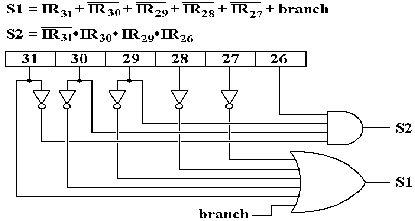
We now define this signal as S2 = ![]() · IR29 · IR26.
· IR29 · IR26.
This is the original definition for signal S2
in the hardwired control unit.
S2 = 1 if and only if the instruction can enter defer and has the indirect bit
set.
S1
We now define this signal as S1 = 1 if and only if the
instruction is to be dispatched
by the microinstruction at address 0x23.
The only instruction that should not be dispatched is
the branch instruction, BR, when the branch condition is 0. Dispatch under one of two conditions; either
1. IR31IR30IR29IR28IR27
¹ 01111, or
2. IR31IR30IR29IR28IR27
= 01111 and branch = 1.
Our circuit design sets S1 = 0 if and only if
IR31IR30IR29IR28IR27
= 01111 and branch = 0.
Generating
Signals S1 and S2
We still use hardwired logic to generate signals used
by the microprogram.
S2 = 1 if and only if the next microinstruction should
implement defer.
Newly
Labeled “Type 0” Microinstruction
By the label “type 0” we mean instructions with
micro–opcode = 0
that exist only to emit control signals.
Here is the format with the new labels.
|
Micro–Op |
B1 |
B2 |
B3 |
ALU |
M1 |
M2 |
S2 = 0 |
S2 = 1 |
|
4 bits |
4 bits |
4 bits |
4 bits |
4 bits |
4 bits |
4 bits |
8 bits |
8 bits |
A
little thought will lead to the conclusion that most microinstructions do not
test this
S2 bit, which is used only to test for entering the Defer phase.
Despite
being unused, the bit S2 will always have a value; either S2 = 0 or S2 = 1.
For these microinstructions, the address of the next
microinstruction will not depend on the value of S2. In these cases the address for S2 = 0 will
duplicate that for S2 = 1.
As an example, we show the microinstructions for the
first four instructions.
|
Address |
Micro-Op |
B1 |
B2 |
B3 |
ALU |
M1 |
M2 |
S2 = 0 |
S2 = 1 |
|
0x00 |
0 |
0 |
0 |
0 |
0 |
0 |
1 |
0x20 |
0x20 |
|
0x01 |
0 |
4 |
0 |
3 |
1 |
0 |
2 |
0x20 |
0x20 |
|
0x02 |
0 |
4 |
3 |
3 |
7 |
0 |
0 |
0x20 |
0x20 |
|
0x03 |
0 |
1 |
3 |
3 |
5 |
0 |
2 |
0x20 |
0x20 |
Instruction
Fetch and Dispatch
Here is what we have so far on the “common fetch”
microprogram segment.
Next
Address
Address Micro–Op Control Signals S2
= 0 S2 = 1
0x20 0 PC ® B1, tra1, B3 ® MAR, READ. 0x21 0x21
0x21 0 PC ® B1, 1 ® B2, add, B3 ® PC. 0x22 0x22
0x22 0 MBR ® B2, tra2, B3 ® IR. 0x23 0x23
0x23 1 Dispatch based on the opcode. 0x20 0x20
The
instruction in address 0x23 is the only “type 1” microinstruction in the whole
design.
More than that, it is the only microinstruction that
is not a “type 0”.
The micro–control unit will be designed to execute
this type of instruction as follows.
If S1 = 1 the next address is the opcode, found in
the IR (Instruction Register)
If S1 = 0 the next address will be found in the NA 0
field.
This
will be the first address of the fetch sequence. We leave this
as
a field in the microcode to allow for flexibility in design.
The
Micro–Control Unit
The function of the micro–control unit is to sequence
the execution of the microprogram. Its
only function is to select the address to be placed into the mMAR, the address for the micro–memory. All of the logic is contained in a Select
unit, a modified multiplexer.
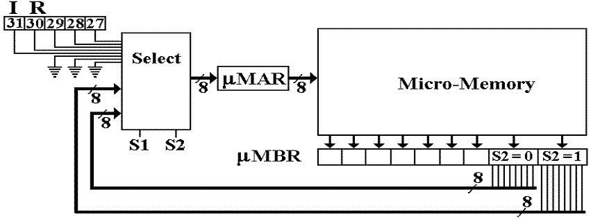
If S1 = 1 then
000¢IR31–27 is placed into the mMAR.
If S1 = 0 and S2 = 0 then
the address associated with field S2 = 0 is used.
If S1 = 0 and S2 = 1 then
the address associated with field S2 = 1 is used.
All that is missing is a provision to jam 0x20 into
the mMAR upon system startup.
Summary of
the Microinstruction Format
Here is the format of the microinstruction.
|
Micro–Op |
B1 |
B2 |
B3 |
ALU |
M1 |
M2 |
S2 = 0 |
S2 = 1 |
|
4 bits |
4 bits |
4 bits |
4 bits |
4 bits |
4 bits |
4 bits |
8 bits |
8 bits |
Here are
the bus and ALU assignments
|
Code |
Bus 1 |
Bus 2 |
Bus 3 |
ALU |
|
0 |
|
|
|
|
|
1 |
PC ® B1 |
1 ® B2 |
B3 ®PC |
tra1 |
|
2 |
MAR ® B1 |
– 1 ®B2 |
B3 ® MAR |
tra2 |
|
3 |
R ® B1 |
R ® B2 |
B3 ®R |
shift |
|
4 |
IR ® B1 |
|
B3 ® IR |
not |
|
5 |
SP ® B1 |
|
B3 ® SP |
add |
|
6 |
|
MBR ® B2 |
B3 ® MBR |
sub |
|
7 |
|
IOD ®B2 |
B3 ® IOD |
and |
|
8 |
|
|
B3 ® IOA |
or |
|
9 |
|
|
|
xor |
|
A |
|
|
|
|
Summary of
the Microinstruction Format (Part 2)
Here again is the format of the microinstruction.
|
Micro–Op |
B1 |
B2 |
B3 |
ALU |
M1 |
M2 |
S2 = 0 |
S2 = 1 |
|
4 bits |
4 bits |
4 bits |
4 bits |
4 bits |
4 bits |
4 bits |
8 bits |
8 bits |
The bits associated with the M1 field are
those specifying the shift parameters
Bit 3 L
/ ![]() (1 for a
left shift, 0 for a right shift)
(1 for a
left shift, 0 for a right shift)
Bit 2 A (1
for an arithmetic shift)
Bit 1 C (1 for circular shift)
Bit 0 Not used
The bits
associated with the M2 field are
Bit 3 READ (Indicates a memory reference)
Bit 2 WRITE (Unless
READ = 1)
Bit 1 extend (Sign–extend contents of IR when
copying to B1)
Bit 0 0
® RUN (Stop the computer)
Microprogram
Example 1: Instructions 0x00 – 0x07
HLT Op-Code
= 00000 0 ® RUN.
|
Address |
Micro-Op |
B1 |
B2 |
B3 |
ALU |
M1 |
M2 |
S2 = 0 |
S2 = 1 |
|
0x00 |
0 |
0 |
0 |
0 |
0 |
0 |
1 |
0x20 |
0x20 |
LDI Op-Code
= 00001 IR ® B1, extend, tra1, B3 ® R.
|
Address |
Micro-Op |
B1 |
B2 |
B3 |
ALU |
M1 |
M2 |
B = 0 |
B = 1 |
|
0x01 |
0 |
4 |
0 |
3 |
1 |
0 |
2 |
0x20 |
0x20 |
ANDI Op-Code
= 00010 IR ® B1, R ® B2, and, B3 ® R.
|
Address |
Micro-Op |
B1 |
B2 |
B3 |
ALU |
M1 |
M2 |
B = 0 |
B = 1 |
|
0x02 |
0 |
4 |
3 |
3 |
7 |
0 |
0 |
0x20 |
0x20 |
ADDI Op-Code
= 00011 IR ® B1, R ® B2, extend, add, B3 ® R.
|
Address |
Micro-Op |
B1 |
B2 |
B3 |
ALU |
M1 |
M2 |
B = 0 |
B = 1 |
|
0x03 |
0 |
1 |
3 |
3 |
5 |
0 |
2 |
0x20 |
0x20 |
Opcodes 00100 through 00111
|
Address |
Micro-Op |
B1 |
B2 |
B3 |
ALU |
M1 |
M2 |
B = 0 |
B = 1 |
|
|
0 |
0 |
0 |
0 |
0 |
0 |
0 |
0x20 |
0x20 |
Micro–memory
Layout: Instructions 0x00 – 0x07
Based on the tables above, we state the contents of
the first eight micro–words.
|
Address |
Contents |
|
0x00 |
0x
000 0001 2020 |
|
0x01 |
0x
040 3102 2020 |
|
0x02 |
0x
043 3700 2020 |
|
0x03 |
0x
013 3502 2020 |
|
0x04 |
0x
000 0000 2020 |
|
0x05 |
0x
000 0000 2020 |
|
0x06 |
0x
000 0000 2020 |
|
0x07 |
0x
000 0000 2020 |
Each
micro–memory word contains 44 bits, expressed as 11 hexadecimal digits.
This design allows for future definition of assembly
language instructions for
the opcodes 0x04 through 0x07.
The current design calls for each of these four
opcodes to be a NOP, doing nothing.
Microprogram
for LDR (Load Register)
IR ® B1, R ® B2, add, B3 ® MAR
|
Address |
Micro-Op |
B1 |
B2 |
B3 |
ALU |
M1 |
M2 |
S2 = 0 |
S2 = 1 |
|
0x0C |
0 |
4 |
3 |
2 |
5 |
0 |
0 |
0x2F |
0x2C |
Defer
Begins: READ
|
Address |
Micro-Op |
B1 |
B2 |
B3 |
ALU |
M1 |
M2 |
S2 = 0 |
S2 = 1 |
|
0x2C |
0 |
0 |
0 |
0 |
0 |
0 |
8 |
0x2D |
0x2D |
WAIT
|
Address |
Micro-Op |
B1 |
B2 |
B3 |
ALU |
M1 |
M2 |
S2 = 0 |
S2 = 1 |
|
0x2D |
0 |
0 |
0 |
0 |
0 |
0 |
0 |
0x2E |
0x2E |
MBR ® B2, tra2, B3 ® MAR
|
Address |
Micro-Op |
B1 |
B2 |
B3 |
ALU |
M1 |
M2 |
S2 = 0 |
S2 = 1 |
|
0x2E |
0 |
0 |
6 |
2 |
2 |
0 |
0 |
0x2F |
0x2F |
Execute
Begins: READ.
|
Address |
Micro-Op |
B1 |
B2 |
B3 |
ALU |
M1 |
M2 |
S2 = 0 |
S2 = 1 |
|
0x2F |
0 |
0 |
0 |
0 |
0 |
0 |
8 |
0x30 |
0x30 |
WAIT.
|
Address |
Micro-Op |
B1 |
B2 |
B3 |
ALU |
M1 |
M2 |
S2 = 0 |
S2 = 1 |
|
0x30 |
0 |
0 |
0 |
0 |
0 |
0 |
0 |
0x31 |
0x31 |
MBR ® B2, tra2, B3 ® R
|
Address |
Micro-Op |
B1 |
B2 |
B3 |
ALU |
M1 |
M2 |
S2 = 0 |
S2 = 1 |
|
0x31 |
0 |
0 |
6 |
3 |
2 |
0 |
0 |
0x20 |
0x20 |
Structure of
the Microprogram for LDR (Part 1)
We now show the entire sequence, beginning at the
common fetch.
The common fetch with the new dispatch instruction is
shown first.
|
Address |
Micro-Op |
B1 |
B2 |
B3 |
ALU |
M1 |
M2 |
S2 = 0 |
S2 = 1 |
|
0x20 |
0 |
1 |
0 |
2 |
1 |
0 |
8 |
0x21 |
0x21 |
|
0x21 |
0 |
1 |
1 |
1 |
5 |
0 |
0 |
0x22 |
0x22 |
|
0x22 |
0 |
0 |
6 |
4 |
2 |
0 |
0 |
0x23 |
0x23 |
|
0x23 |
1 |
0 |
0 |
0 |
0 |
0 |
0 |
0x20 |
0x20 |
The
Dispatch Instruction, at address 0x023, represents a design change from the
original Boz–5. In the new design, the
next address depends on the discrete signal S1.
If S1 = 0, the address of the next instruction will be
0x20 (the contents of S2 = 0)
This
causes an immediate fetch of the next instruction when the conditions
for a branch are
not met.
If S1 = 1, the address of the next instruction will be
the 5–bit opcode,
extended to eight bits
by prefixing it with “000”.
The opcode for LDR is 01100, or 0x0C.
Structure of
the Microprogram for LDR (Part 2)
The instruction at address 0x0C (the opcode for LDR)
completes the indexing and does a conditional branch, depending on the value of
the flag S2.
If S2 = 1, indirect addressing is used, and the
If S2 = 0, indirect addressing is not used, and the
IR ® B1, R ® B2, add, B3 ® MAR
|
Address |
Micro-Op |
B1 |
B2 |
B3 |
ALU |
M1 |
M2 |
S2 = 0 |
S2 = 1 |
|
0x0C |
0 |
4 |
3 |
2 |
5 |
0 |
0 |
0x2F |
0x2C |
Earlier
designs of the Boz–5 performed the “branch test” at this point.
The “branch test”, in which it is determined if the
instruction is a conditional branch for which the condition has not been met,
is now assigned to the dispatch instruction (0x23).
For all “type 0” instructions, the two addresses
determine the next instruction whenever indirect addressing is used and
whenever it is not used.
The Defer microcode for LDR begins at address 0x2C.
The Execute microcode for LDR begins at address 0x2F.
Note that the Defer microprogram always “falls
through” into the Execute microprogram, as the Defer phase is always followed
by the Execute phase.
Structure of
the Microprogram for LDR (Part 3)
Defer
Begins:
READ
|
Address |
Micro-Op |
B1 |
B2 |
B3 |
ALU |
M1 |
M2 |
S2 = 0 |
S2 = 1 |
|
0x2C |
0 |
0 |
0 |
0 |
0 |
0 |
8 |
0x2D |
0x2D |
WAIT
|
Address |
Micro-Op |
B1 |
B2 |
B3 |
ALU |
M1 |
M2 |
S2 = 0 |
S2 = 1 |
|
0x2D |
0 |
0 |
0 |
0 |
0 |
0 |
0 |
0x2E |
0x2E |
MBR ® B2, tra2, B3 ® MAR
|
Address |
Micro-Op |
B1 |
B2 |
B3 |
ALU |
M1 |
M2 |
S2 = 0 |
S2 = 1 |
|
0x2E |
0 |
0 |
6 |
2 |
2 |
0 |
0 |
0x2F |
0x2F |
Execute
Begins:
READ.
|
Address |
Micro-Op |
B1 |
B2 |
B3 |
ALU |
M1 |
M2 |
S2 = 0 |
S2 = 1 |
|
0x2F |
0 |
0 |
0 |
0 |
0 |
0 |
8 |
0x30 |
0x30 |
WAIT.
|
Address |
Micro-Op |
B1 |
B2 |
B3 |
ALU |
M1 |
M2 |
S2 = 0 |
S2 = 1 |
|
0x30 |
0 |
0 |
0 |
0 |
0 |
0 |
0 |
0x31 |
0x31 |
MBR ® B2, tra2, B3 ® R
|
Address |
Micro-Op |
B1 |
B2 |
B3 |
ALU |
M1 |
M2 |
S2 = 0 |
S2 = 1 |
|
0x31 |
0 |
0 |
6 |
3 |
2 |
0 |
0 |
0x20 |
0x20 |
Upgraded
Handling of the Defer Phase
The
textbook design focuses on the proper handling of the BR (Branch) instruction
but did not place that decision in the proper context. Only the dispatch microinstruction at address
0x23 needs to handle this condition. The
new design reflects this.
The
structure of the textbook microprogram reflects a much older design that had to
use explicit branching instructions to handle the Defer state. This structure predates your instructor’s
introduction to explicit inclusion of the next micro–address.
Your
instructor discovered this newer design while reading the textbook Structured
Computer Organization by Andrew S. Tanenbaum (ISBN 0–13–148521–0).
The
older design called for coding such as the following for the LDR.
0x0C 0 IR
® B1, R ® B2, add,
B3 ® MAR; Go to 0x2C
0x2C 2 If
D = 0 Go to 0x30. If D = 1 Go to 0x2D.
0x2D 0 The
defer state begins here. Execute begins
at 0x30.
The newer design
eliminates the explicit conditional branch and its associated wasted time by
using the two–next–address structure that is now part of the design.
0x0C 0 IR
® B1, R ® B2, add,
B3 ® MAR;
Go
to 0x2C if D = 1, else go to 0x2F.
Note that Execute for LDR in the new design begins at
address 0x2F.
Two
Different Handlings of LDR
Older
Version (as in the textbook)
Address Micro–Op Instruction
0x0C 0 IR
® B1, R ® B2, add,
B3 ® MAR; Go to 0x2C
0x2C 2 If
D = 0 Go to 0x30. If D = 1 Go to 0x2D.
0x2D 0 READ;
Go to 0x2E
0x2E 0 WAIT;
Go to 0x2F
0x2F 0 MBR
® B2, tra2, B3 ® MAR; Go to 0x30
0x30 0 READ;
Go to 0x31
0x31 0 WAIT;
Go to 0x32
0x32 0 MBR
® B2, tra2, B3 ® R; Go to 0x20
Newer
Version
Address Micro–Op Instruction
0x0C 0 IR
® B1, R ® B2, add,
B3 ® MAR;
If
D = 0 Go to 0x2F. If D = 1 Go to 0x2C.
0x2C 0 READ;
Go to 0x2D
0x2D 0 WAIT;
Go to 0x2E
0x2E 0 MBR
® B2, tra2, B3 ® MAR; Go to 0x2F
0x2F 0 READ;
Go to 0x30
0x30 0 WAIT;
Go to 0x31
0x31 0 MBR
® B2, tra2, B3 ® R; Go to 0x20