Major and
Minor States
We now consider the micro–operations and control
signals associated
with the execution of each instruction in the ISA.
The execution of each instruction is divided into
three phases.
These phases are called “major states”. They are:
1. Fetch: The
instruction is fetched from memory.
2. Defer: This
phase handles the computation of indirect addresses.
3. Execute: The
instruction is executed and the result stored.
Each major state is broken into a number of minor states,
each with duration of one clock pulse.
In the hardwired control unit, each major state will
comprise four minor states,
called T0, T1, T2, and T3.
This inflexible design is due to the simplicity of the
control unit.
In the microprogrammed control unit, each of these major
states is just suggestive,
corresponding to a section of the microcode.
Each state in the microcode takes as many clock pulses
as necessary.
The
Hardwired Control Unit: Basis for Design
As stated above, the hardwired control unit issues
control signals based on:
1. The op–code in bits 31 – 27 of the IR
(Instruction Register).
2. The ALU condition flags: N, Z, and C.
3. The Major State: one of Fetch, Defer, or
Execute.
4. The Minor State: one of T0, T1, T2, or T3.
The 5–bit op–code is an input to a 5–to–32
decoder. Each of the outputs of this
decoder
is associated with and labeled by an instruction in the ISA.
Boolean control signals emitted by this decoder are
HLT, LDI, ANDI, ADDI, GET, PUT,
RET, RTI, LDR, STR, JSR, BR, LLS, LCS, RLS, RAS, NOT, ADD, SUB, AND, OR,
and XOR. Each of these corresponds to
the related assembly language instruction.
Example: The assembly language instruction ADD has op–code
10101 (decimal 21).
When
the input to the decoder is 10101, then the output Y21 is activated.
This output is the
Boolean control signal ADD; ADD = 1.
When
ADD = 1, the op–code is that for the ADD instruction.
All other signals are Boolean and have value either 0 or 1. Thus we can say Fetch = 1
when the major state is Fetch, T2 = 1 when the minor state is T2, etc.
The Hardwired
Control Unit: Sequencing the States
In the hardwired control unit, each of the major state
and the minor state must progress
in a predictable sequence.
The minor state sequence is fixed and predictable; it
is shown in the figure below.
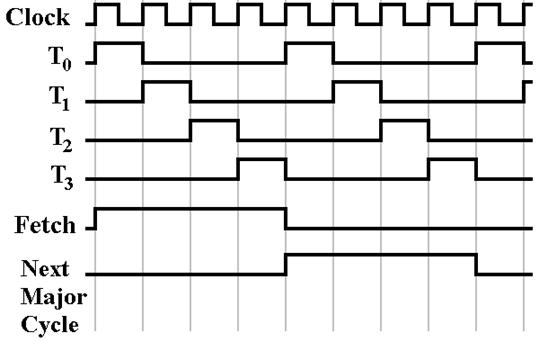
Here we see that each minor state is active for
exactly the duration of one clock pulse.
The
Note that the minor state register continuously
repeats the sequence T0, T1, T2, T3, etc.
It is a modulo–4 counter. Here is the implementation of the minor state
register
as a “one hot” modulo–4 counter. The
signal “Start” initializes the counter.
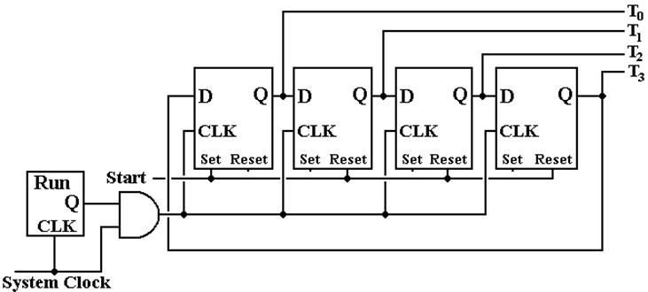
When the run flip–flop is set, the clock pulses get
through to the state register
and cause it to count.
When the run flip–flop is reset (Q = 0), clock pulses are no longer fed
to the counter
and the minor state becomes static.
Sequencing
the Major State Register
The major state register might easily be considered a
modulo–3 counter with values
00 Fetch denoted
by “F” in these notes
01 Defer denoted by “D” in these notes
10 Execute denoted by “E” in these notes
In this design the major states move in sequence: F,
D, E, F, D, E, F, D, E, etc.
This extremely simple design is very wasteful. Why spend four clock times in the Defer
state if the instruction does not use indirect addressing, the only reason for
that state.
So we now consider modification of the minor state
register so that
When
indirect addressing is used, the state following Fetch is Defer
When
indirect addressing is not used, the state following Fetch is not Defer.
Does this modification imply that the state following
Fetch is either Defer or Execute
depending on whether or not indirect addressing is used?
This is not necessarily so. We have another trick up our sleeve.
The Common
Fetch Sequence and Its Implications
Here is a slight restatement of the control signals
for the common fetch sequence.
F, T0: PC ® B1, tra1, B3 ® MAR, READ. // MAR ¬ (PC)
F, T1: PC ® B1, 1 ® B2, add, B3 ® PC. //
PC ¬ (PC) + 1
F, T2: MBR ® B2, tra2, B3 ® IR. // IR ¬ (MBR)
F, T3: // Do something related to the instruction.
As we shall see, many of the instructions can be
executed in one clock pulse.
We
now ask ourselves the following question.
If the execution of an instruction can be
completed in the Fetch phase, why enter the Execute phase and waste four clock
cycles.
The answer is simple: there is no reason.
We
now ask the first question about sequencing the major state register.
What state follows Fetch?
If the instruction
execution can be completed in Fetch, the next state is Fetch.
If it cannot
be completed in Fetch and indirect addressing used, the next state is Defer.
If it cannot
be completed in Fetch and indirect addressing is not used,
the next state is Execute.
More on the
Major State Register
What we have discovered is as follows.
1. The minor state register is a simple
modulo–four counter.
As long
as the computer is running, this counter continues to produce output.
The
sequence is always the same: T0, T1, T2, T3, T0, T1, T2, T3, etc.
Note
that each minor state is labeled by the control signal that is active.
T0: T0 = 1 T1
= 0 T2 = 0 T3 = 0
T1: T0 = 0 T1
= 1 T2 = 0 T3 = 0, etc.
2. The
major state register is a modified modulo–three counter.
The
sequence always begins with Fetch, but the next major state after
a given one depends on the
instruction being executed.
Each
major state has Boolean control signals associated.
Fetch: F = 1 D = 0 E = 0
Defer: F = 0 D = 1 E = 0
Execute: F
= 0 D = 0 E = 1.
In order to design the major state register, we must
first examine the sequence of
microoperations (and control signals) associated with each instruction in the
ISA.
Top–Level
View of the ALU
In our previous discussions, we have seen the need for
the ALU to respond to the
following three control signals.
tra1 transfer
the contents of bus B1 to bus B3.
tra2 transfer
the contents of bus B2 to bus B3.
add add
the contents of busses B1 and B2, place the sum on bus B3.
Examination of the register–to–register operations
shows the necessity of additional
control signals to the ALU in order to execute the instructions.
shift needed
by the shift operations LLS, LCS, RLS, RAS
The type
of shift is determined by additional control signals
not needed
by the logical not operation
sub needed by the subtraction operation
or needed
by the logical OR operation
and needed
by the logical AND operation
xor needed by the logical
exclusive OR operation
Given this, let’s examine the control signals,
beginning with the register operations.
Overview of
Register–To–Register Operations
The structure of the Fetch phase of all
register–to–register operations follows
a simple common pattern.
F, T0 – F, T2: This
is the common fetch sequence.
All
instructions share this part.
F, T3: Source
register or source registers placed on the bus structure
Command
the ALU with the appropriate control signal
Transfer
bus B3 to the destination register.
For dyadic operations, we have SR2 ® B2 and SR1 ® B1.
For monadic operations, we have SR ® B2.
The
ALU commands are one of those listed on the previous slide, but repeated here:
shift (with
the shift type specified by control signals L/![]() , A, and C)
, A, and C)
not
add, sub, or, and, xor
Monadic
Register–To–Register Operations (Part 1)
Each of these instructions can be executed in one
clock pulse, so that
the execution is completed in the Fetch phase, with no Defer or Execute.
The type of shift is determined by three Boolean
control signals.
L / ![]() : If L /
: If L / ![]() = 0, this is a right
shift. If L /
= 0, this is a right
shift. If L / ![]() = 1, it is a left
shift.
= 1, it is a left
shift.
A, C: If C = 1, this is a circular shift. The A flag is not used here.
If
C = 0 and A = 1, this is an arithmetic shift.
If
C = 0 and A = 0, this is a logical shift.
Note that a shift cannot be both circular and arithmetic.
This implies a convention for handling the case in
which A = 1 and C = 1.
The fact that the control unit should never assert
these two signals does not remove
the necessity for designing for this eventuality.
The design decision here is that the circular flag
takes precedence, so that
C = 1,
A = 0 this is a circular shift
C = 1,
A = 1 this is also a circular shift
Monadic
Register–To–Register Operations (Part 2)
Left Shifts
LLS Op-Code = 10000 (Hexadecimal 0x10)
F, T0: PC ® B1, tra1, B3 ® MAR, READ. // MAR ¬ (PC)
F, T1: PC
® B1, 1 ® B2, add, B3 ® PC. //
PC ¬ (PC) + 1
F, T2: MBR
® B2, tra2, B3 ® IR. // IR ¬ (MBR)
F, T3: R
® B2, shift, L / ![]() = 1, A = 0. C = 0, B3 ® R.
= 1, A = 0. C = 0, B3 ® R.
LCS Op-Code = 10001 (Hexadecimal 0x11)
F, T0: PC ® B1, tra1, B3 ® MAR, READ. // MAR ¬ (PC)
F, T1: PC
® B1, 1 ® B2, add, B3 ® PC. //
PC ¬ (PC) + 1
F, T2: MBR
® B2, tra2, B3 ® IR. // IR ¬ (MBR)
F, T3: R
® B2, shift, L / ![]() = 1, A = 0. C = 1, B3 ® R.
= 1, A = 0. C = 1, B3 ® R.
When
we implement the shifter, we shall cause left arithmetic shifts to be
equivalent to left logical shifts, so that for left shifts we have the
following:
C = 0 logical
left shift (without regard to the value of the A flag).
C = 1 circular left shift (without regard to
the value of the A flag).
Monadic
Register–To–Register Operations (Part 3)
Right Shifts and Logical Negation
RLS Op-Code = 10010 (Hexadecimal 0x12)
F, T0: PC ® B1, tra1, B3 ® MAR, READ. // MAR ¬ (PC)
F, T1: PC
® B1, 1 ® B2, add, B3 ® PC. //
PC ¬ (PC) + 1
F, T2: MBR
® B2, tra2, B3 ® IR. // IR ¬ (MBR)
F, T3: R
® B2, shift, L / ![]() = 0, A = 0. C = 0, B3 ® R.
= 0, A = 0. C = 0, B3 ® R.
RAS Op-Code = 10011 (Hexadecimal 0x13)
F, T0: PC ® B1, tra1, B3 ® MAR, READ. // MAR ¬ (PC)
F, T1: PC
® B1, 1 ® B2, add, B3 ® PC. //
PC ¬ (PC) + 1
F, T2: MBR
® B2, tra2, B3 ® IR. // IR ¬ (MBR)
F, T3: R
® B2, shift, L / ![]() = 0, A = 1. C = 0, B3 ® R.
= 0, A = 1. C = 0, B3 ® R.
NOT Op-Code = 10100 (Hexadecimal 0x14)
F, T0: PC ® B1, tra1, B3 ® MAR, READ. // MAR ¬ (PC)
F, T1: PC
® B1, 1 ® B2, add, B3 ® PC. //
PC ¬ (PC) + 1
F, T2: MBR
® B2, tra2, B3 ® IR. // IR ¬ (MBR)
F, T3: R
® B2, not, B3 ® R.
Dyadic
Register–To–Register Operations
Arithmetic Operations
ADD Op-Code = 10101 (Hexadecimal 0x15)
F, T0: PC ® B1, tra1, B3 ® MAR, READ. // MAR ¬ (PC)
F, T1: PC
® B1, 1 ® B2, add, B3 ® PC. //
PC ¬ (PC) + 1
F, T2: MBR
® B2, tra2, B3 ® IR. // IR ¬ (MBR)
F, T3: R
® B1, R ® B2, add,
B3 ® R.
SUB Op-Code = 10110 (Hexadecimal 0x16)
F, T0: PC ® B1, tra1, B3 ® MAR, READ. // MAR ¬ (PC)
F, T1: PC
® B1, 1 ® B2, add, B3 ® PC. //
PC ¬ (PC) + 1
F, T2: MBR
® B2, tra2, B3 ® IR. // IR ¬ (MBR)
F, T3: R
® B1, R ® B2, sub,
B3 ® R.
Dyadic
Register–To–Register Operations
Boolean Operations
AND Op-Code = 10111 (Hexadecimal 0x17)
F, T0: PC ® B1, tra1, B3 ® MAR, READ. // MAR ¬ (PC)
F, T1: PC
® B1, 1 ® B2, add, B3 ® PC. //
PC ¬ (PC) + 1
F, T2: MBR
® B2, tra2, B3 ® IR. // IR ¬ (MBR)
F, T3: R
® B1, R ® B2, and,
B3 ® R.
OR Op-Code = 11000 (Hexadecimal 0x18)
F, T0: PC ® B1, tra1, B3 ® MAR, READ. // MAR ¬ (PC)
F, T1: PC
® B1, 1 ® B2, add, B3 ® PC. //
PC ¬ (PC) + 1
F, T2: MBR
® B2, tra2, B3 ® IR. // IR ¬ (MBR)
F, T3: R
® B1, R ® B2, or, B3
® R.
XOR Op-Code = 11001 (Hexadecimal 0x19)
F, T0: PC ® B1, tra1, B3 ® MAR, READ. // MAR ¬ (PC)
F, T1: PC
® B1, 1 ® B2, add, B3 ® PC. //
PC ¬ (PC) + 1
F, T2: MBR
® B2, tra2, B3 ® IR. // IR ¬ (MBR)
F, T3: R
® B1, R ® B2, xor, B3 ® R.
Immediate
Mode Operations (Part 1)
HLT Op-Code = 00000 (Hexadecimal 0x00)
F, T0: PC ® B1, tra1, B3 ® MAR, READ. // MAR ¬ (PC)
F, T1: PC
® B1, 1 ® B2, add, B3 ® PC. //
PC ¬ (PC) + 1
F, T2: MBR
® B2, tra2, B3 ® IR. // IR ¬ (MBR)
F, T3: 0
® RUN. // Reset the RUN Flip-Flop
At
this point, the sequencing of the major and minor states stops.
Memory and register contents are preserved for manual
debugging.
The next state will be (F, T0) whenever the computer
is restarted.
LDI Op-Code = 00001 (Hexadecimal 0x01)
F, T0: PC ® B1, tra1, B3 ® MAR, READ. //
MAR ¬ (PC)
F, T1: PC
® B1, 1 ® B2, add, B3 ® PC. // PC ¬ (PC) + 1
F, T2: MBR
® B2, tra2, B3 ® IR. //
IR ¬ (MBR)
F, T3: IR
® B1, extend, tra1, B3 ® R. // Copy IR19-0
as signed integer
Immediate
Mode Operations (Part 2)
ANDI Op-Code = 00010 (Hexadecimal 0x02)
F, T0: PC ® B1, tra1, B3 ® MAR, READ. //
MAR ¬ (PC)
F, T1: PC
® B1, 1 ® B2, add, B3 ® PC. //
PC ¬ (PC) + 1
F, T2: MBR
® B2, tra2, B3 ® IR. //
IR ¬ (MBR)
F, T3: IR
® B1, R ® B2, and,
B3 ® R. // Copy IR19-0 as 20 bits.
// The 20 bits IR19-0
are copied without extension, so we have in reality
// 0000 0000 0000 ¢ IR19-0
® B1. This may be changed in a future design.
ADDI Op-Code = 00011 (Hexadecimal 0x03)
F, T0: PC ® B1, tra1, B3 ® MAR, READ. //
MAR ¬ (PC)
F, T1: PC
® B1, 1 ® B2, add, B3 ® PC. //
PC ¬ (PC) + 1
F, T2: MBR
® B2, tra2, B3 ® IR. //
IR ¬ (MBR)
F, T3: IR
® B1, R ® B2, extend,
add, B3 ® R. // Add signed integer
NOTE: Up to this
point, every instruction examined can be executed in one clock
cycle
following the three clock cycles needed to fetch it.
Fourteen
of the twenty–two instructions can be so executed.
RISC Design:
A Side Note
Let us imagine a standard Reduced Instruction Set Computer
(RISC) design with a
well–functioning instruction prefetch unit.
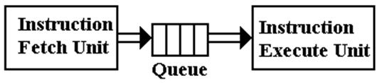
Here we assume that the prefetch
unit maintains a queue of instructions that are ready
to be run by the execution unit and immediately available for transfer to the
IR.
Under these circumstances, there is no fetch penalty
for an instruction.
Put another way, the common fetch sequence discussed
above goes away and
each of the previous fourteen instructions could be executed in one clock cycle
total time.
Whenever one sees the design goal of one instruction
executed per clock cycle in the
early RISC designs, it is this phenomenon that is being described.
Later superscalar
designs, with multiple execution units, aim to execute multiple
instructions per clock cycle.
Instructions
That Use the Execute Cycle
Here we note a division in the instruction set.
There
are 14 instructions that can be executed in one clock cycle.
These can be completed in the
Fetch phase.
The
remaining 8 instructions require more than one clock cycle to
complete execution. These 8 must be extended into the Execute
Cycle.
These eight that require “extra time” for execution
are:
01000 GET Input
into a general purpose register.
01001 PUT Output
from a general purpose register.
01010 RET Return
from subroutine.
01011 RTI Return
from an interrupt handler.
01100 LDR Load
general purpose register from memory.
01101 STR Store
general purpose register into memory.
01110 JSR Call
subroutine.
01111 BR Branch
(Jump), either conditionally or unconditionally.
The fact that these instructions share the “01” prefix will be used
later in
the design of the part of the control unit that sequences the major state
register.
The Input
and Output Instructions: Assumptions
At some point in the implementation of these two
instructions, we must allow for the
fact that these two operations are basically asynchronous to the CPU.
To illustrate this point, consider two instructions
STR and PUT.
STR store
register to memory.
The
memory timings are known and fixed. The
microoperation sequence
that implements this
instruction is designed to allow for the memory cycle time.
PUT copy
register to an output device.
The
timings for the output device are quite variable, and can appear random.
The
microoperation sequence must depend on a signal from the output device
that it is ready to accept
data; otherwise output data will be lost.
One way to handle this is to set up a “handshaking protocol” using one or
more
D flip–flops to signal availability of data and readiness to transfer that
data.
The Boz–5 design is based on device interrupts.
An
input device interrupts when it has data ready for input.
An
output device interrupts when it can accept more data.
This removes the complexity of the handshake.
The Input
and Output Instructions: Implementation
For
each of these two instructions, the design calls for execution that requires
two clock cycles. Neither can be
completed within the Fetch phase.
Since
completion in the Fetch phase is not possible, we remove all of the execution
steps
to the Execute phase. This will simplify
the control unit in that Fetch will be simpler.
We
now ask ourselves how to place two microoperations into four time slots. Placement
into slots T0 and T2 is somewhat arbitrary, though less likely to cause
difficulties.
GET Op-Code = 01000 (Hexadecimal 0x08)
F, T0: PC ® B1, tra1, B3 ® MAR, READ. //
MAR ¬ (PC)
F, T1: PC
® B1, 1 ® B2, add, B3 ® PC. // PC ¬ (PC) + 1
F, T2: MBR
® B2, tra2, B3 ® IR. //
IR ¬ (MBR)
F, T3: WAIT.
E, T0: IR ® B1, tra1,
B3 ® IOA. // Send out the I/O address
E, T1: WAIT.
E, T2: IOD
® B2, tra2, B3 ® R. // Get the
results.
E, T3: WAIT.
Again, note the assumption in (E, T2) that the input
data has data ready to transfer.
Implementation
of the Put Instruction
PUT Op-Code = 01001 (Hexadecimal 0x09)
F, T0: PC ® B1, tra1, B3 ® MAR, READ. //
MAR ¬ (PC)
F, T1: PC
® B1, 1 ® B2, add, B3 ® PC. // PC ¬ (PC) + 1
F, T2: MBR
® B2, tra2, B3 ® IR. //
IR ¬ (MBR)
F, T3: WAIT.
E, T0: R ® B2, tra2,
B3 ® IOD // Get the data ready
E, T1: WAIT.
E, T2: IR
® B1, tra1, B3 ® IOA. //
Sending out the address
E, T3: WAIT. // causes the output of data.
Here again, we assume that the output device can
accept the data when it is sent out.
The control sequence in (E, T2) may be incomplete. Were this actually implemented,
we might discover the need for another control signal to affect the output.
Output causes the addressed output unit to
copy the data from its
bus data
register into its internal data registers.
NOTE: Neither GET nor PUT involve a memory address.
Three
Instructions: JSR, RET, and RTI
We shall postpone the discussion of the
subroutine–related instructions (JSR and RET)
until we have developed a strategy for subroutine linkage.
We mention in passing the difference between the two
instructions RET and RTI.
At one level, the two instructions seem to be
identical. Each involves a return from
a subprogram that was executed to achieve a specific purpose.
The main difference is due to the nature of an
interrupt and depends on the details
of handling an interrupt.
It is possible to specify a structure in which
interrupts are handled in the same way
as subroutine calls. In that case we do
not need two return instructions.
On the Boz–5, the implementation of the RTI instruction
is yet to be defined.
We specify two return instructions, RET and RTI, just
to show that there might
be a difference.
Address
Computation: Preconditions on the Execute Phase
We have four instructions that use an Effective Address in memory.
LDR Load a general–purpose register from the
memory at the effective address.
STR Store a general–purpose register into
memory at the effective address.
JSR Jump to the subroutine at the effective
address.
BR Branch to the memory at the effective
address.
What these instructions have in common is the use of
an effective address.
We stipulate a simple precondition on the Execute
Phase.
The Effective Address will be in the MAR (Memory Address Register).
This gives rise to a postcondition on the Fetch phase:
it must leave an address in
the MAR.
Design of
the Defer State: Preconditions and Postconditions
Due to the precondition on Execute, each of Fetch and
Defer must
leave an address in the MAR.
Our scheme is based on two assumptions:
1. Pre–indexed addressing is used; indexing is
done before indirection.
2. The Defer State handles only computation of
indirect addressing.
These observations lead to conditions on both Fetch
and Defer.
Fetch Postcondition A properly indexed address is placed
into the MAR.
Defer Precondition The MAR holds an address.
Postcondition The MAR holds an address that
correctly implements
the
indirection.
If indirect addressing is not used,
the
If indirect addressing is used,
the
based on the indexed address computed
in Fetch.
Control
Signals for the Defer State
The
The I–bit is IR26.
The common “signature” of these four instructions is
the prefix “011”.
When IR31 = 0, IR30 = 1, and IR29 = 1, we have
one of these four instructions.
The
Here
are the control signals for Defer.
D, T0: READ. //
Address is already in the MAR.
D, T1: WAIT. //
Cannot access the MBR just now.
D, T2: MBR
® B2, tra2, B3 ® MAR. // MAR ¬ (MBR)
D, T3: WAIT. //
Effective Address is now in the MAR.
Remember
the precondition on the
The condition is that the properly indexed address is
in the MAR.
If indirect addressing is used, then the MAR contains not the address
of the argument,
but the address of a pointer to the argument.
The memory at that address must be read
in order to obtain the address of the argument, which is then deposited into
the MAR.
Control
Signals for Load Register
Here is the complete set of control signals for LDR.
LDR Op-Code = 01100 (Hexadecimal 0x0C)
F, T0: PC ® B1, tra1, B3 ® MAR, READ. // MAR ¬ (PC)
F, T1: PC
® B1, 1 ® B2, add, B3 ® PC. //
PC ¬ (PC) + 1
F, T2: MBR
® B2, tra2, B3 ® IR. // IR ¬ (MBR)
F, T3: IR
® B1, R ® B2, add,
B3 ® MAR. //
Do the indexing.
Here the
major state register takes control.
1) If the I–bit (bit 26) is 1, then the Defer
state is entered.
2) If
the I–bit is 0, then the E state is
entered.
D, T0: READ. //
Address is already in the MAR.
D, T1: WAIT. // Cannot
access the MBR just now.
D, T2: MBR
® B2, tra2, B3 ® MAR. // MAR ¬ (MBR)
D, T3: WAIT.
The Execute
state is entered either from Fetch or Defer.
E,
T0: READ. //
The Effective Address is in the MAR.
E, T1: WAIT. // Just
read the memory at that address, wait,
E, T2: MBR
® B2, tra2, B3 ® R. // and then
transfer its contents to the register.
E, T3: WAIT.
Control
Signals for Store Register
Here is the complete set of control signals for STR.
STR Op-Code = 01101 (Hexadecimal 0x0D)
F, T0: PC ® B1, tra1, B3 ® MAR, READ. // MAR ¬ (PC)
F, T1: PC
® B1, 1 ® B2, add, B3 ® PC. //
PC ¬ (PC) + 1
F, T2: MBR
® B2, tra2, B3 ® IR. // IR ¬ (MBR)
F, T3: IR
® B1, R ® B2, add,
B3 ® MAR. //
Do the indexing.
D, T0: READ.
D, T1: WAIT.
D, T2: MBR
® B2, tra2, B3 ® MAR.
D, T3: WAIT.
E, T0: WAIT.
E, T1: R
® B1, tra1, B3 ® MBR, WRITE. // This could be
in T0 or T2.
E, T2: WAIT. //
Do not place the WRITE in T3
E, T3: WAIT. //
we want it done by the end of T3.
In (E, T1) we send the contents of the source register
to bus B1.
The reason given in the textbook is that bus B2 has been allocated for
the index register.
However, the indexed addressing has already been computed; this allocation to
B1 may
not be required. We shall just use it
anyway as it causes no problems.
Conditional
Branching: Use of the Major State Register
The branch instruction starts execution just as every
other instruction that uses a
memory address and might use an indirect memory address.
Here is the complete fetch sequence for the BR
instruction.
BR Op-Code = 01111 (Hexadecimal 0x0F)
F, T0: PC ® B1, tra1, B3 ® MAR, READ. // MAR ¬ (PC)
F, T1: PC
® B1, 1 ® B2, add, B3 ® PC. //
PC ¬ (PC) + 1
F, T2: MBR
® B2, tra2, B3 ® IR. // IR ¬ (MBR)
F, T3: IR
® B1, R ® B2, add,
B3 ® MAR. //
Do the indexing.
At
the end of (F, T3) two things are known.
1. We have a conditional branch instruction.
Remember an unconditional branch
is branch if 1 = 1, which always holds.
2. We have the values of the flags (N, Z, and C)
from the previous operation,
so we know whether or not the
branch will be taken.
If branch =
0, the state following Fetch is again
Fetch.
The branch is not
taken; the next instruction is fetched.
If branch =
1, the state following Fetch is either Defer or Execute; the branch is taken.
Control
Signals for the Branch Instruction
BR Op-Code = 01111 (Hexadecimal 0x0F)
F, T0: PC ® B1, tra1, B3 ® MAR, READ. // MAR ¬ (PC)
F, T1: PC
® B1, 1 ® B2, add, B3 ® PC. //
PC ¬ (PC) + 1
F, T2: MBR
® B2, tra2, B3 ® IR. // IR ¬ (MBR)
F, T3: IR
® B1, R ® B2, add,
B3 ® MAR. //
Do the indexing.
Here the Major State Register takes control. If the control signal Branch = 1, then the
following is executed. If the control
signal Branch = 0, the next instruction is fetched.
D, T0: READ.
D, T1: WAIT.
D, T2: MBR
® B2, tra2, B3 ® MAR.
D, T3: WAIT.
E, T0: WAIT.
E, T1: WAIT.
E, T2: WAIT.
E, T3: MAR
® B1, tra1, B3 ® PC. // To jump, place a
new address into the PC.