The
General–Purpose Register Set
A
schematic of the general–purpose registers of the Boz–5 is shown below.
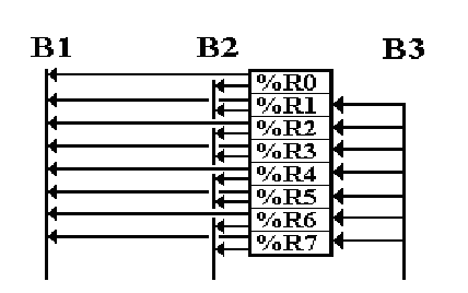
Connection
of these registers to the CPU data busses is controlled as follows:
Signal Field Comment
R ® B1 B1S When R ® B1 is asserted, the three–bit field B1S
selects
the register to be connected to bus B1.
R ® B2 B2S When
R ® B2 is asserted, the three–bit field B2S
selects
the register to be connected to bus B2.
B3
® R B3D When B3 ® R is asserted,
the three–bit field B3D
selects
the register to receive the contents of bus B3.
How to
Generate the Register Selector Fields?
The
question for this lecture concerns the generation of each of these three–bit
fields
B1S, B2S, and B3D.
Obviously,
these will be based on bit fields in the Instruction Register.
The
actual circuitry for generating each of these fields depends on the
structure of the binary machine instructions.
Outline for this lecture:
1. Determine the register usage for each class
of assembly language instructions.
2. Discuss one simple microarchitecture with a
very simple structure.
Mention why that one was not
selected.
3. Discuss the part of the Boz–5
microarchitecture that actually
generates the fields B1S, B2S,
and B3D.
In
determining the register usage, we shall consider:
First,
the simple register operations, and
then,
the memory reference operations that complicate the situation.
Register Use
Survey: Dyadic Register Operations
These
operations involve two source registers and one destination register.
The
generic machine code template for these instructions is as follows:
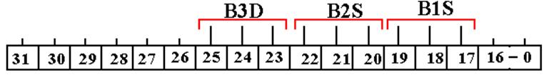
|
31 |
30 |
29 |
28 |
27 |
26 |
25 |
24 |
23 |
22 |
21 |
20 |
19 |
18 |
17 |
16
– 0 |
|
Op–Code |
|
Destination Register |
Source Register 2 |
Source Register 1 |
Not used |
||||||||||
This “reverse numbering” of
Source Register 2 and Source Register 1 was
made in order to make the design of the control unit hardware easier to read.
The
operations in this class are ADD DR ¬ (SR2) + (SR1)
SUB DR ¬ (SR2) – (SR1)
AND DR ¬ (SR2) Ù (SR1)
OR DR ¬ (SR2) Ú (SR1)
XOR DR ¬ (SR2) Å (SR1)
Here
the generation of the fields is obvious: B3D
= IR25–23
B2S
= IR22–20
B1S
= IR19–17
Register Use
Survey: Monadic Register Operations
These
operations involve one source register and one destination register.
The
generic machine code template for these instructions is as follows:
|
31 |
30 |
29 |
28 |
27 |
26 |
25 |
24 |
23 |
22 |
21 |
20 |
19 |
18 |
17 |
16 |
15 |
14 – 0 |
|
Op–Code |
|
Destination Register |
Source Register |
Shift Count |
Not Used |
||||||||||||
The operations in this class
are LLS DR ¬ Left logical shift of SR
LCS DR ¬ Left circular shift of SR
RLS DR
¬ Right logical shift of
SR
RAS DR ¬ Right arithmetic shift of SR
NOT DR ¬ One’s complement of SR
The
destination register is fed by bus B3, so one choice is simple: B3D = IR25–23.
We
now ask which bus will the source register feed?
The
simple answer comes from the fact that the source register is specified in IR22–20,
so we allocate this source register to bus B2 and again let B2S = IR22–20.
Register Use
Survey: Register Load and Store
The
register–to–register instructions seem to suggest and simple, almost trivial,
way to generate the fields B1S, B2S, and B3D.
The
only problem with this occurs with the Store
Register to Memory instruction.
Consider
the two instructions LDR and STR.
LDR (Load Register from Memory)
This
requires two registers: a destination
register for the load, and
an
index register for use in computing the address.
STR (Store Register into Memory)
This
requires two registers: a source
register for the data to go into memory, and
an
index register for use in computing the address.
We
can place the index register on either bus B1 or bus B2, using either B1S or
B2S to identify it as appropriate.
Note: LDR has a destination
register
STR has a source register.
Memory
Reference Operations: Option 1
Here
we shall present a design decision that lead to the current microarchitecture.
The
simplest option is to have each instruction have fields for three registers;
call them DR, SR2, and SR1. Arbitrarily
let SR1 indicate the Index Register.
Here
is what the situation for LDR would be.
|
Op–Code |
I–bit |
DR |
SR2 |
SR1 |
Address |
|
01100 |
|
Destination |
Not Used |
Index Register |
Address Field |
Here is what the situation for
STR would be
|
Op–Code |
I–bit |
DR |
SR2 |
SR1 |
Address |
|
01101 |
|
Not Used |
Source |
Index Register |
Address Field |
The advantage of this design is
extremely simple logic for generating B1S, B2S, & B3D.
The
disadvantage of this design is either fewer registers or a smaller address
space.
(More on this later).
Memory
Reference Operations: Option 2
The
next option is to have a single field, called “Source / Destination”, that
contains the destination register for LDR and the source register for STR.
Here
is what the situation for LDR would be.
|
Op–Code |
I–bit |
Source / Destination |
SR2 |
Address |
|
01100 |
|
Destination Register |
Index Register |
Address Field |
Here is what the situation for
STR would be
|
Op–Code |
I–bit |
Source / Destination |
SR2 |
Address |
|
01101 |
|
Source Register |
Index Register |
Address Field |
This design allows more
bits for the address field, but leads to a slight increase
in the complexity of the control circuitry for B1S and B3D.
We
now consider each design option in turn.
The one given is easily stated:
1. We
have a 32–bit instruction word
2. We
have allocated five bits for the op–codes and one bit for the I–bit.
3. This
leaves us 26 bits to specify the registers and address field.
More on
Instruction Format 1
Here
is the first option considered, in which each instruction contains fields for
all three register selector fields: B1S, B2S, and B3D.
|
Bits |
31 – 27 |
26 |
25 – 0 (Twenty six bits) |
|||
|
Use |
Op–Code |
I-Bit |
DR |
SR2 |
SR1 |
Address Field |
The eight–register option
This
requires three bits to select each register.
This
means nine bits for the register selection, so allows 17 bits for the address
field.
The
direct address space is 0 through 217 – 1 or 0 through 131, 071.
This
leads to an interesting number of registers, but a very small address space.
The four–register option
This
requires two bits to select each register.
This
means six bits for the register selection, so allows 20 bits for the address
field.
The
direct address space is 0 through 220 – 1 or 0 through 1, 048, 576.
This
preserves the Boz–5 address space, but cuts the number of registers.
Register
Selection Fields for Instruction Format 1
(Assuming eight general–purpose registers)
In
this arrangement, the generation of the three register select fields is easy.
Here
is the diagram for the circuitry.
Here is the RTL description of
the generation of these register–select fields.
B3D ¬ IR25–23
B2S ¬ IR22–20
B1S ¬ IR19–17
Register
Selection Fields for Instruction Format 1
(Continued)
Here
are some register allocations for instructions under this assumption.
Instruction IR25–23 IR22–20 IR19–17 IR16–0
HLT 000 000 000 Not
used
LDI Destination Not Used Not
Used 17–bit signed integer
ANDI DR SR2 SR1 17–bit
mask
ADDI DR SR2 SR1 17–bit
signed integer
GET DR Not used Not used 17–bit
I/O address
PUT Not
used Source Not used 17–bit I/O address
LDR Destination Not used Index
Register 17–bit address field
STR Not
used Source Index Register 17–bit address field
JSR Not
used Not used Index Register 17–bit address field
BR Branch Not used Index Register 17–bit
address field
Condition
Monadic Destination Source Shift
Count Not used
Dyadic Destination SR2 SR1 Not used
Register
Selection Fields for Instruction Format 2
(Assuming eight general–purpose registers)
We
return to the option of having a single
field, called “Source / Destination”.
Here
is what the situation for LDR would be.
|
Op–Code |
I–bit |
Source / Destination |
SR2 |
Address |
|
01100 |
|
Destination Register |
Index Register |
Address Field |
Here is what the situation for
STR would be
|
Op–Code |
I–bit |
Source / Destination |
SR2 |
Address |
|
01101 |
|
Source Register |
Index Register |
Address Field |
Assuming eight general–purpose registers, the IR
layout becomes
|
Bits |
31 – 27 |
26 |
25 – 23 |
22 – 20 |
19 – 0 |
|
Use |
Op–Code |
I–bit |
Source / Destination |
Index |
Address |
This
is the basic structure of the machine language instructions in the present
design.
The
additional complexity in the control unit is due to the necessity of
interpreting
IR25–23 as a source register for exactly one instruction – STR.
Register
Selection Fields for the Boz–5
We
now work our way through the instruction set and see how the structure of the
machine language for each instruction will dictate the generation of the three
fields used to select the general–purpose registers: B1S, B2S, and B3D.
Immediate Addressing
|
31 |
30 |
29 |
28 |
27 |
26 |
25 |
24 |
23 |
22 |
21 |
20 |
19 – 0 |
|
Op–Code |
|
Destination Register |
Source |
Immediate Argument |
||||||||
Here are the four
immediate–mode instructions
Op–Code
00000 HLT Halt (Actually, this has no operands)
00001 LDI Load
Immediate (Does not use Source Register)
00010 ANDI Immediate
logical AND
00011 ADDI Add
Immediate
For
each of these, we have B3D = IR25–23
The
last two instructions, ANDI and ADDI, use a source register designated by bits
IR22–20 in the Instruction Register.
We have two possible source busses, so that this could indicate either
bus B1 or B2.
For
compatibility with the register–to–register instructions, we say B2S = IR22–20.
Register
Selection Fields for the Boz–5 (Part 2)
Input/Output Instructions
This design calls for isolated I/O,
so it has dedicated input and output instructions.
Input
Op-Code 01000 GET Get a 32–bit word into a destination
register from an input.
|
31 |
30 |
29 |
28 |
27 |
26 |
25 |
24 |
23 |
22 |
21 |
20 |
19 |
18 |
17 |
16 |
15 – 0 |
|
0 |
1 |
0 |
0 |
0 |
|
Destination |
Not Used |
Not Used |
I/O Address |
|||||||
Use
B3D = IR25–23
Output
Op-Code 01001 PUT Put a 32–bit word from a source register to an
output register.
|
31 |
30 |
29 |
28 |
27 |
26 |
25 |
24 |
23 |
22 |
21 |
20 |
19 |
18 |
17 |
16 |
15 – 0 |
|
0 |
1 |
0 |
0 |
1 |
|
Not Used |
Source |
Not Used |
I/O Address |
|||||||
Use
B2S = IR22–20
Register
Selection Fields for the Boz–5 (Part 3)
We
now examine the register instructions that reference memory.
Load
Register
|
31 |
30 |
29 |
28 |
27 |
26 |
25 |
24 |
23 |
22 |
21 |
20 |
19 – 0 |
|
0 |
1 |
1 |
0 |
0 |
I bit |
Destination Register |
Index Register |
Address |
||||
The obvious option for the
destination register field is to set B3D = IR25–23.
If we place the index register
contents onto bus B2, we can retain B2S = IR22–20.
Store
Register
|
31 |
30 |
29 |
28 |
27 |
26 |
25 |
24 |
23 |
22 |
21 |
20 |
19 – 0 |
|
0 |
1 |
1 |
0 |
1 |
I bit |
Source Register |
Index Register |
Address |
||||
Here we also retain the choice
of bus B2 for the index register, so B2S = IR22–20.
Note that bits IR25–23
specify a source register. We have only
one more source bus,
so we must say that B1S = IR25–23.
Register
Selection Fields for the Boz–5 (Part 4)
We
now consider the subroutine call and branch instructions.
Subroutine
Call
|
31 |
30 |
29 |
28 |
27 |
26 |
25 |
24 |
23 |
22 |
21 |
20 |
19 – 0 |
|
0 |
1 |
1 |
1 |
0 |
I bit |
Not Used |
Index |
Address |
||||
This is rather easy to
handle, as there is no source or destination register.
The
index register transfer is easily handled by setting B2S = IR22–20.
Branch
|
31 |
30 |
29 |
28 |
27 |
26 |
25 |
24 |
23 |
22 |
21 |
20 |
19 – 0 |
|
0 |
1 |
1 |
1 |
1 |
I bit |
Branch |
Index |
Address |
||||
Again, we set B2S = IR22–20
to handle the indexing.
The
three–bit branch condition, stored in IR25–23, is sent directly to
the control unit.
More on the
Branch Conditions
The
branch condition codes for the design are as follows.
Code Action Code Action
000 Branch
Always 100 Branch if carry–out is 0
001 Branch
on negative result 101 Branch if result not negative
010 Branch
on zero result 110 Branch if result is not zero
011 Branch
if result not positive 111 Branch on positive result
Note that the conditions are arranged in pairs. With the exception of the first row
(for codes 000 and 100) each row contains opposite conditions.
This “opposite structure” is a result of an attempt to
simplify the logic in the control unit.
The control unit operates based on a signal, called “Branch”, that is output from an
8–to–1 multiplexer with selector input from IR25–23.
When
the output of the MUX is Branch = 1, the branch is taken.
Implementation
of the Branch Condition
The
branch instruction is implemented using a multiplexer in the control unit.
The
input to this multiplexer includes the following:
+1 this
is always true, used for unconditional branches,
N the
negative bit from the ALU, set if the last ALU result was negative,
Z the
zero bit from the ALU, set if the last ALU result was zero,
C the
carry bit from the ALU, set if there was a carry–out from the ALU

Register
Selection Fields for the Boz–5 (Part 5)
Unary Register-To-Register
|
31 |
30 |
29 |
28 |
27 |
26 |
25 |
24 |
23 |
22 |
21 |
20 |
19 |
18 |
17 |
16 |
15 |
14 – 0 |
|
Op–Code |
|
Destination Register |
Source Register |
Shift Count |
Not Used |
||||||||||||
Here we
have B3D = IR25-23 and B2S = IR22-20.
Opcode = 10000 LLS Logical
Left Shift
10001 LCS Circular
Left Shift
10010 RLS Logical
Right Shift
10011 RAS Arithmetic
Right Shift
10100 NOT Logical
NOT (Shift count ignored)
Register
Selection Fields for the Boz–5 (Part 6)
|
31 |
30 |
29 |
28 |
27 |
26 |
25 |
24 |
23 |
22 |
21 |
20 |
19 |
18 |
17 |
16 – 0 |
|
Op–Code |
|
Destination Register |
Source Register 2 |
Source Register 1 |
Not used |
||||||||||
Opcode = 10101 ADD Addition
10110 SUB Subtraction
10111 AND Logical AND
11000 OR Logical
OR
11001 XOR Logical
Exclusive OR
This
uses the complete set of register selection fields.
B3D = IR25–23
B2S = IR22–20
B1S = IR19–17
Summary of
the Register Selector Fields
The following table summarizes the requirements levied
by the instructions on the generation of the control signals B1S, B2S, and B3D.
|
|
B1S |
B2S |
B3D |
|
HLT |
|
|
|
|
LDI |
|
|
IR25-23 |
|
ANDI |
|
IR22-20 |
IR25-23 |
|
ADDI |
|
IR22-20 |
IR25-23 |
|
GET |
|
|
IR25-2 |
|
PUT |
|
IR22-20 |
|
|
LDR |
|
IR22-20 |
IR25-23 |
|
STR |
IR25-23 |
IR22-20 |
|
|
BR |
|
IR22-20 |
|
|
JSR |
|
IR22-20 |
|
|
RET |
|
|
|
|
RTI |
|
|
|
|
Monadic Register |
|
IR22-20 |
IR25-23 |
|
Dyadic Register |
IR19-17 |
IR22-20 |
IR25-23 |
The only design issue is that B1S = IR25–23
for the STR instruction,
and B1S = IR19–17 for every other instruction, even it if is not
used.
Generating
the Register Selector Fields
Here
is the complete circuit.
It
is rather busy, so we show two simplifications.
For some instructions, the
logic generates values for a field that is not used by the control logic. If the field is not used, it does not matter
if its value is nonsensical.
Generating
the Register Selector Fields (Part 2)
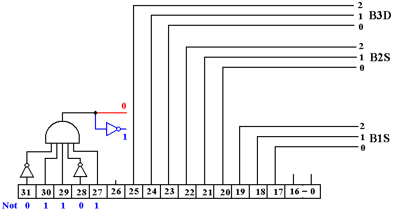
STR Op–Code = 01101
Here is the effective circuit when IR31-27
= 01101.
The selector B3D is not used as the control signal B3 ® R is not asserted.
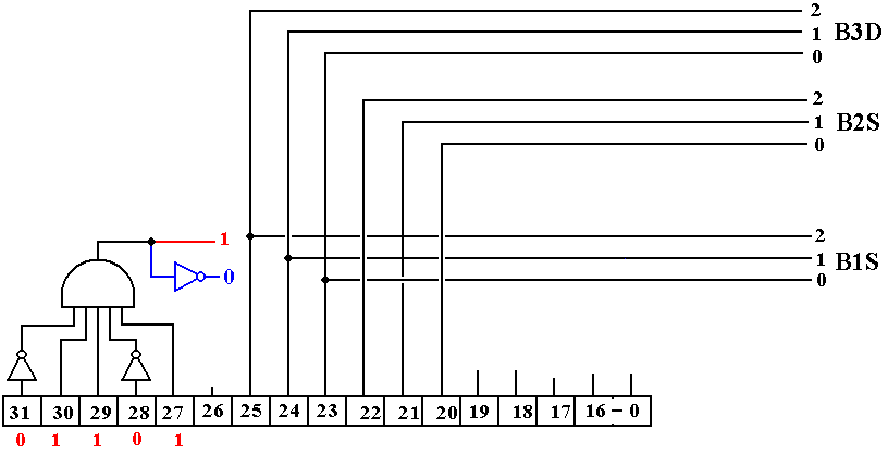
Note:
The field B3D is generated here, but is not used.
Generating
the Register Selector Fields (Part 3)
Other
Op–Codes
Here is the effective circuit for
other instructions.
Two
Addressing Modes: Direct and Indexed
Remember
that register R0 is defined to be exactly 0; %R0 º 0.
Consider
direct addressing and indexed addressing.
The syntax of the assembly language calls for indexed addressing to be
used when the index field is not 0.
Put
one way: If IR22IR21IR20
= 000, then direct addressing is used, and
if IR22IR21IR20
¹ 000, then indexed
addressing is used.
Put
another way, we have
IR22IR21IR20
= 000 MAR ¬ IR19–0 + 0
IR22IR21IR20
= 001 MAR ¬ IR19–0 + (%R1)
IR22IR21IR20
= 010 MAR ¬ IR19–0 + (%R2)
IR22IR21IR20
= 011 MAR ¬ IR19–0 + (%R3)
IR22IR21IR20
= 100 MAR ¬ IR19–0 + (%R4)
IR22IR21IR20
= 101 MAR ¬ IR19–0 + (%R5)
IR22IR21IR20
= 110 MAR ¬ IR19–0 + (%R6)
IR22IR21IR20
= 111 MAR ¬ IR19–0 + (%R7)
Summary of
the Reduction in Addressing Modes
Using
the %R0 º 0 trick, the four
addressing modes collapse into two modes.
|
|
Indexed by %R0 |
Indexed by another register |
|
Indirection Not Used, IR26 = 0 |
Direct |
Indexed |
|
Indirection Used, IR26 = 1 |
Indirect |
Indexed-Indirect |