Review of
Instruction Fetch
We
have discussed the common fetch sequence in previous lectures.
We
have given both the sequence of microoperations and the corresponding sequence
of control signals. Remember that memory
timings restrict access to memory during the
(Fetch, T1) time slot, so we elect to update the Program Counter during this
time.
Fetch,
T0: (PC) ® B1, tra1,
B3 ® MAR, READ.
Fetch,
T1: (PC) ® B1, 1 ® B2, add,
B3 ® PC.
Fetch,
T2: (MBR) ® B2, tra2,
B3 ® IR.
This lecture focuses on the
impact of incrementing the program counter on
1) the design of the ALU, and
2) the bus structure of the CPU.
It
is immediately obvious that the ALU must have either an addition operation or
an increment (add 1) operation. For
simplicity, the design uses a simple addition operation, associated with the
control signal “add”.
We
have always assumed that the CPU has three internal data busses.
We now show why such a
configuration is desirable.
Constraints
Due to the ALU
Recall
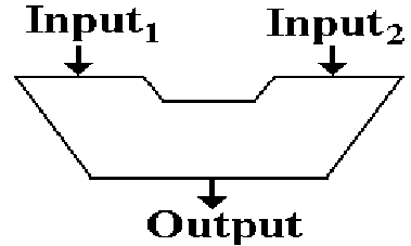
that the ALU itself has two inputs and one output.
We
consider how to create a bus structure for the CPU that will make efficient
use of this ALU. For this discussion, we
focus on the addition operation
associated with updating the PC (Program Counter).
One–Bus
Design for the CPU
The
simplest design for the CPU calls for one common internal bus.
The
restriction that only one binary data set can be on a single bus at
any given time gives rise to severe timing problems.
Specifically,
it will take two clock pulses to put the two arguments (PC and 1)
on the bus and one clock pulse to transfer the updated value to the PC.
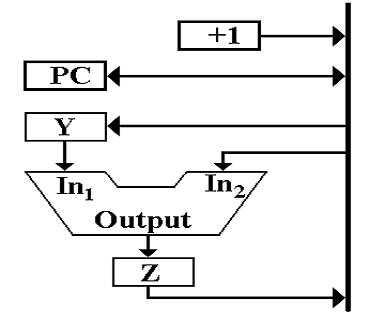
This
one–bus design calls for two holding registers, here called “Y” and “Z”.
 The control signals required for this structure are:
T1: 1 ® Bus, Bus ® Y.
T2: PC ® Bus, add.
T3: Z ® Bus, Bus ® PC.
The
addition takes three clock pulses.
It
is easy to show that a 2–bus design requires
two clock pulses to perform the addition.
Efficient
Addition Requires a Three–Bus Structure
With
this structure, the CPU can complete the addition in one clock cycle.
This
example is only one case in which the CPU design is considerably simplified
by having a three bus structure.
It can be seen that having
three internal busses only modestly increases the design
complexity of the CPU. This is considered
a good trade–off.
Immediate
Implications of the Three–Bus Design
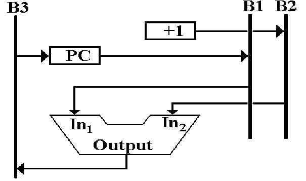
The
design of the CPU calls for it to have three internal busses.
These
are called B1, B2, and B3.
B1
and B2 serve as input busses for the ALU.
B3
serves as an output bus for the ALU.
This design can be seen
in another light.
B1
and B2 are the only busses to which any register can transfer data directly.
B3
is the only bus that can transfer data directly to any register.
The protocol for
register–to–register transfer becomes as follows:
1. Transfer from the source register to either
bus B1 or bus B2 (but not both).
2. Signal the ALU to connect the appropriate
input bus to bus B3.
3. Transfer the contents of bus B3 to the
destination register.
This
implies two additional ALU control signals: tra1
and tra2
tra1 transfer
the contents of B1 to B3
tra2 transfer
the contents of B2 to B3
More
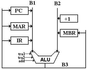
Requirements of the Common Fetch Sequence
Let’s repeat the common fetch
sequence and examine it for more requirements.
Fetch, T0: (PC) ® B1, tra1,
B3 ® MAR, READ.
Fetch, T1: (PC) ® B1, 1 ® B2, add,
B3 ® PC.
Fetch,
T2: (MBR) ® B2, tra2,
B3 ® IR.
T0: We have handled the requirements for bus
transfer. This demands the signal
tra1 to the ALU. The READ
control signal goes to the memory interface.
T1: We have handled these requirements completely.
T2: Here we have two more registers to be assigned
to input busses.
My earlier designs required that
the Memory Buffer Register and Instruction
Register be assigned to different
busses, so this design reflects that.
Connecting
the IR to Bus B1
The
structure of the IR (Instruction Register) calls for bits to be sent directly
to the Control Unit and bits to be sent to the bus B1.
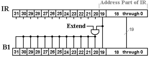
We
focus on the twenty lower order bits of the IR: IR19 – IR0.
In
some instructions these bits IR19 – IR0 form an address
for accessing memory.
In
some instructions these bits IR19 – IR0 are interpreted
as an immediate operand,
either a 20–bit (five hexadecimal digit) bit mask,
or a 20–bit two’s–complement
signed integer.
In
some instructions, bits IR19
– IR17 are part of the instruction and
bits
IR16 – IR0 are not used.
In
any case, provision is made to transfer only bits IR19 – IR0
to bus B1.
This
transfer is enabled by the signal IR ® B1.
Sign
Extension in Connecting the IR to Bus B1
Two
of the immediate instructions, LDI and ADDI, require the contents of bits IR19
– IR0 to be sign extended and treated as a 32–bit two’s–complement
integer.
The
other instructions that use bits IR19 – IR0 treat them as
an unsigned integer.
To
handle this we have a control signal “Extend”,
which is emitted by the control unit.
Here
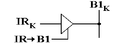
is a representation of the transfer mechanism for the IR.
Labeling
Control Signals
Control
signals are Boolean signals with two values:
Logic 1 Usually
asserted as + 5 volts.
Logic 0 Usually asserted as 0 volts.
Each
control signal is labeled by the action that it enables.
IR ® B1 This
signal enables the transfer of IR19 – IR0 to bus B1.
It might
be called IR19–0 ® B1
Extend When
IR ® B1 is asserted, this
causes the transfer to
be sign
extended.
Control
signals that enable data transfers to either bus B1 or bus B2 will take
effect by enabling a tri–state buffer.
The IR is one of many possible inputs to B1.
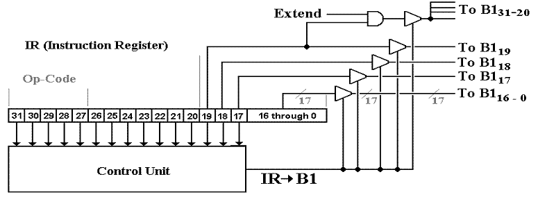
The Complete
Connection Scheme for the Instruction Register
Here
is a schematic that shows the basic processes associated with the transfer.
The
Control Unit emits both signals (Extend and IR ® B1). Only the
latter is shown explicitly, due to a desire to keep the figure uncluttered.
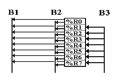
The General
Purpose Registers
In
this version of the design, the CPU has eight general–purpose registers.
R0 This
register is read–only, holding the value 0.
R1 – R7 These seven registers are read/write and can be used for any
purpose.
They are often
used as index registers.
Each
of these eight registers can output to either bus B1 or bus B2.
Bus
B3 can place data into any of the seven registers R1 – R7, but is not connected
to R0.
The Complete
Register Set
Here
is the complete register set and bus structure for the CPU. Note the two special purpose constant
registers +1 and –1, used by the Control Unit.
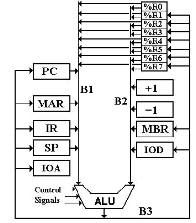
Attaching
the General Purpose Registers to the Bus Structure
There
are only three control signals emitted by the Control Unit that enable these
transfers. These are:
R ® B1 The selected register is copied to bus B1.
R ® B2 The selected register is copied to bus B2.
B3 ® R The contents of bus B3 are copied into the selected
register.
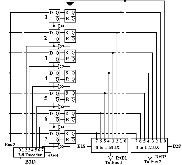
We
now ask how each of these registers is selected.
The
Control Unit uses three selector registers, each based on bit fields in the IR.
The generation of these selector registers will be discussed later.
B1S This
selects the register to be placed on B1 when R ® B1 is asserted.
B2S This
selects the register to be placed on B2 when R ® B2 is asserted.
B3D This
selects the register to copy the contents of B3
when B3 ® R is asserted.
If B3D = 000, no transfer occurs.
Each
of the signals B1S and B2S is the control input to an 8–to–1 multiplexer that
outputs to a bus through a tri–state buffer enabled by the appropriate control
signal.
The signal B3D is the 3–bit
input to an active–high 3–to–8 decoder that is
enabled by the control signal B3 ® R.
Figure:
Connecting a Single Bit to the Busses
Comments on
the Connection
Transfer to a register.
When
control signal B3 ® R is asserted, the 3–to–8 decoder is activated and asserts the clock
input of all flip–flops associated with the selected register.
Each
flip–flop associated with the selected register takes input from its bit line
on B3.
Output
0 of the decoder is not connected to any register, so that asserting
B3 ® R when B3D = 000 has no
effect.
If
B3 ® R is not asserted, all
decoder outputs are 0 and nothing happens.
Transfer from a register.
Note
that the selector registers B1S and B2S always have values, so that the output
of the multiplexer associated with each bus always copies some general–purpose
register.
When
control signal R ® B1 is asserted the selected register is output to bus B1.
If it is not asserted, either B1 is not active or a special purpose register is
feeding it.
When
control signal R ® B2 is asserted the selected register is output to bus B2.
If it is not asserted, either B2 is not active or a special purpose register is
feeding it.
It
is expected that the two signals R ® B1 and R ® B2 can be asserted simultaneously.