Operation of the Control Unit
Topics:
1. Structure and Function of the Control Unit.
2. Review of the Common Fetch Sequence.
2. Structure of the ALU and Its Impact on Control Signals.
3. The Control Signals for the Common Fetch Sequence.
4. A Hardwired Control Unit and Its Common Fetch Sequence.
5. A Microprogrammed Control Unit and Its Common Fetch Sequence.
The Central Processing Unit (CPU)
The
CPU has four main components:
1. The Control Unit (along with the IR) interprets the machine language instruction
and issues the control signals to make the CPU execute it.
2. The ALU (Arithmetic Logic Unit) that does the arithmetic and logic.
3. The Register Set (Register File) that stores temporary results related
to the
computations. There are also Special Purpose Registers used by
the Control Unit.
4. An internal bus structure for communication.
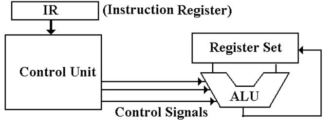
The function of the control
unit is to decode the binary machine word in the IR
(Instruction Register) and issue appropriate control signals, mostly to the
CPU.
Design of the Control Unit
There are two related issues when considering the design of the control unit:
1) the complexity of the Instruction Set Architecture, and
2) the microarchitecture used to implement the control unit.
The
ISA (Instruction Set Architecture) of a computer is
the set of assembly language
commands that the computer can execute. It can be seen as the interface
between the
software (expressed as assembly language) and the hardware.
The
complexity of the ISA is usually driven by programming–language factors. We
shall discuss these factors in a future lecture.
Experience,
beginning with the IBM S/360 in 1964, has shown that a given ISA may
have many distinct implementations. Indeed, this choice is preferable from a business
viewpoint: faster implementations can have more complex and costly control
units.
The
control unit is difficult to design and test. Once that task is complete, the
design
of the rest of the computer is rather simple.
The ISA is a functional specification of the control unit. Let’s follow that specification.
The Fetch–Execute Cycle
This cycle is the logical basis of all stored program computers.
Instructions are stored in memory as machine language.
Instructions are fetched from memory and then executed.
The
fetch sequence of control signals is common to all instructions. It ends
when the instruction has been decoded (identified) and the control unit is
ready to issue control signals specific to that instruction.
This
cycle is described in many different ways, most of which serve to highlight
additional steps required to execute the instruction. Examples of additional
steps are: Decode the Instruction, Fetch the Arguments, Store the Result, etc.
A
stored program computer is often called a “von Neumann Machine” after one
of the originators of the EDVAC.
This Fetch–Execute cycle is
often called the “von Neumann bottleneck”, as the
necessity for fetching every instruction from memory slows the computer.
Common Fetch Sequence: Top–Level Description
Here
is a top–level description of the common fetch sequence,
written in RTL (Register Transfer Language).
At
this point, we use the vague idea of steps to note that these operations
must be done in a fixed sequence.
Step 1: (PC) ® MAR, READ. // Start a memory read to get instruction
Step 2: (PC) + 1 ® PC. // Update the program counter
Step 3: (MBR) ® IR. // Get instruction into the IR
These steps must be translated
into control signals, which actually operate the
basic gates in the CPU. To do this, we must understand the ALU.
Each
of these steps is often called a microoperation, in that it represents
an
instruction to the microarchitecture level.
Note that step 2 in this sequence invokes addition; it uses the ALU.
Constraints Due to the ALU
Recall from an earlier lecture that the ALU has two inputs and one output.
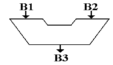
The inputs to the ALU come from two data busses, named “B1” and “B2”.
The
output from the ALU goes to the data bus named “B3”.
Please note that other authors have different names for these internal busses.
At
any one time, only one source register may be placing signals on any given
bus. The use of two input busses implies a maximum of two source registers.
At
any one time, bus B3 can supply more than one destination register. This is
rarely necessary and possibly complex; this design does not use that feature.
More Constraints Due to The ALU
The
only way to communicate via busses is to place data on one of the two
busses (B1 or B2) that input to the ALU, have the ALU transfer the data to bus
B3, and have bus B3 place the data in the destination register.
This
constraint is due to the desire to avoid the complexity associated with
multiple point–to–point transfers of data. The control signals for transfer
are:
tra1 Copy the contents of bus B1 to bus B3
tra2 Copy the contents of bus B2 to bus B3
Thus
the high–level RTL (PC) ® MAR
becomes (PC) ® B1, tra1,
B3 ® MAR.
Aside: A Comment on the Notation
We
use the RTL (Register Transfer Language) both for writing the top–level
microoperations, such as PC ® MAR, and the control signals
that implement
those microoperations, such as PC ® B1, tra1, B3 ® MAR.
The
basic rules for writing RTL are simple:
1. Each line contains one or more transfers that can take place in
any
order or at the same time. Each line ends with a period.
2. We
usually associate each line of RTL with one “time step” and
assume that the transfers take place simultaneously.
3. The
direction of the arrows should be consistent and
indicative of the transfers to take place.
Note that each of the following lines of RTL has the same effect.
(PC) ® B1, tra1, B3 ® MAR.
B1 ¬ (PC), tra1, MAR ¬ B3.
MAR ¬ B3, tra1, B1 ¬ (PC).
Several other variants are possible; each of those is hard to read.
Control Signals for the Common Fetch Sequence
Remember the microoperations for the common fetch sequence.
Step 1: (PC) ® MAR, READ.
Step 2: (PC) + 1 ® PC.
Step 3: (MBR) ® IR.
We
have two source registers shown here: PC and MBR. Each source register
must be associated with exactly one of the input ALU busses, B1 or B2.
At this point we assign the PC to bus B1 and the MBR to bus B2.
The control signals for these three microoperations are as follows.
Step 1: (PC) ® B1, tra1, B3 ® MAR, READ.
Step 2: (PC) ® B1, 1 ® B2, add, B3 ® PC.
Step 3: (MBR) ® B2, tra2, B3 ® IR.
Incrementing the Program Counter
Consider the sequence of control signals to increment the PC.
(PC) ® B1, 1 ® B2, add, B3 ® PC.
We need the ALU to add 1 to the PC and store the value back into the PC.
The
control signal called “add” causes the ALU to add the inputs from the
two
busses B1 and B2. For this reason, we need a constant register in the register
set, called “1” and containing the constant value 1.
Since the PC feeds bus B1, this constant register 1 must feed bus B2.
Another
option would be to create a special ALU instruction, called either
“inc” or “add1”, which adds 1 to the contents of bus B1. We
avoid this as
adding a complexity to the ALU.
Sequencing the Microoperations
We
may infer that the control unit of the CPU executes any given assembly
language instruction by issuing a sequence of microoperations.
The timing of these microoperations is controlled by the system clock.
By
definition, the CPU executes one microoperation (or sequence of control
signals for that microoperation) per clock period.

For
our computer, the rising edge of the system clock will initiate
another microoperation.
The
design question now becomes one of how to organize the “phases” of the
instruction execution so that the control signals can be issued correctly.
We have two options: A hardwired control unit, and
A microprogrammed control unit.
Timing Considerations: Setting the Clock Rate
It
should be obvious that we want the CPU to run at the fastest possible clock
rate
consistent with its ability to cool itself. Faster clocks generate more heat.
Absent
the cooling issue, the controlling factor arises from the signal propagation
times
in the datapath. Mostly these are due to the gate delays of the flip–flops.
Consider
the following diagram, which shows a typical step in the control unit. A
signal
is read from a data storage unit, processed, and placed into a data storage
unit.
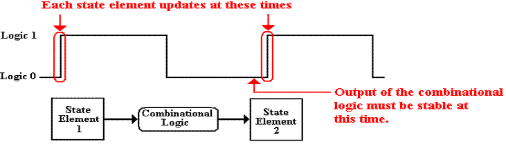
Each
state element is updated on the rising edge of the clock pulse. The clock time
must
be sufficient for the state element to settle, send its output to the
combinational logic
used, and for that combinational logic to generate its output before the next
rising edge.
Timing Considerations: Feedback Loops
Some
of the more important microoperations in the CPU involve a feedback loop: the
output of a register is processed and fed back to that register.
One example is the updating of the Program Counter.
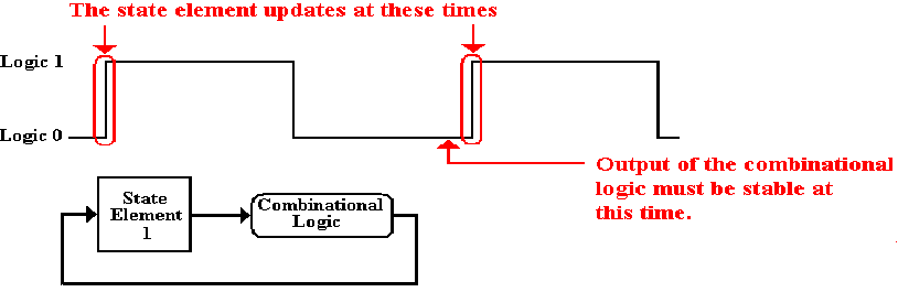
Here
the edge–triggered design allows us to read a register, compute a new value for
it,
and write the contents back in the same clock cycle. By the time that the new
value
arrives at the input of the state element, it is no longer sensitive to its
input. It will not
update from its input until the rising edge of the next clock pulse.
The Logical Basis of the Control Unit
Each
of the two approaches, hardwired control unit and microprogrammed
control unit, addresses the same basic design basis.
Question: What are the inputs to the control unit and what are its outputs?
Inputs
to the control unit must include 1) the instruction being executed, and
2) the condition flags from the ALU. Neither of these is used for this
example.
In
this computer design, the instruction execution is divided into three major
phases, called “Fetch”, “Defer”, and “Execute”.
Fetch the
instruction is fetched and decoded.
If possible, execution is completed in this phase.
Defer the more complex addresses are computed in this phase.
Execute Instructions with memory references complete execution here.
Each
major state is divided into a number of minor states. The duration of a
minor state is, by definition, the clock time of the system clock.
The Hardwired Control Unit (Part 1)
One
common way to generate the control signals is through the use of standard
combinational gates ( AND, OR, NOT ), which output the control signals.
Such
a design will use two special purpose registers:
the Major State Register, and
the Minor State Register.
We
have stipulated three major states: Fetch, Defer, and Execute.
The Major State Register will be implemented as a modulo–3 counter, with
00 = Fetch, 01 = Defer, and 10 = Execute
We
shall see later that the design required four minor states per major state
(although the common fetch uses only three minor states).
These
states will be called T0, T1, T2, and T3; they are generated by a fast
variant of a modulo–4 counter.
This
control unit will use notation such as “Fetch · T0” (logical
AND), which is
1 (TRUE) if and only if Fetch = 1 the major state is Fetch
T0 = 1 the minor state is T0.
The Hardwired Control Unit (Part 2)
Here
is the progression of major states and minor states in a hardwired control
unit, beginning with (Fetch, T0).
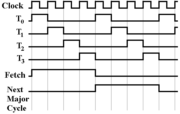
The
top line represents the system clock. The next four represent the states of
the minor state register; each is asserted for one clock period and then
remains at
logic 0 for the next 3. At the end of T3, the next major state is triggered.
Hardwire Control Unit: Control Signals for Common Fetch
Here are the RTL statements for this sequence of control signals.
Fetch, T0: (PC) ® B1, tra1, B3 ® MAR, READ.
Fetch, T1: (PC) ® B1, 1 ® B2, add, B3 ® PC.
Fetch, T2: (MBR) ® B2, tra2, B3 ® IR.
The
conditions to the left of the colon must hold for the control signals on the
line to be executed. These can be read as follows:
If (Fetch = 1) AND (T0 = 1), then (PC) ® B1, tra1, B3 ® MAR, READ.
If (Fetch = 1) AND (T1 = 1), then (PC) ® B1, 1 ® B2, add, B3 ® PC.
If (Fetch = 1) AND (T2 = 1), then (MBR) ® B2, tra2, B3 ® IR.
Another way to read the (Fetch, T0) line is as follows:
If
the major state is Fetch and the minor state is T0, then issue the following
four control signals: (PC) ® B1, tra1, B3 ® MAR, READ.
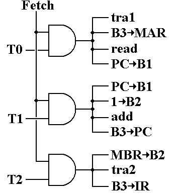
Hardwire Control Unit
Generation of Control Signals for Common Fetch
Here
is the signal generation tree for the control signals associated with the
common Fetch sequence.
The Microprogrammed Control Unit (Part 1)
In
a microprogrammed control unit, the control signals correspond to bits in a
micromemory, which are read into a micro–MBR and emitted.
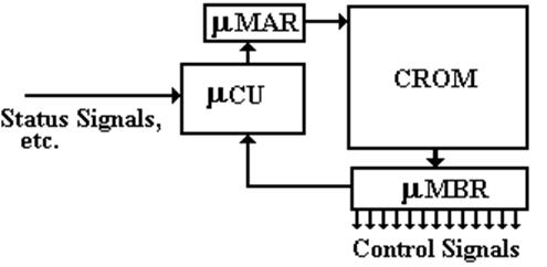
The
micro–control unit ( mCU )
1) places an address into the micro–Memory Address Register ( mMAR ),
2) the control word is read from the Control Read–Only Memory (CROM),
3) into the micro–Memory Buffer Register, and
4) the control signals are issued.
The Microprogrammed Control Unit (Part 2)
In
order to design the control program, we must list the control signals that must
be issued. Restricting ourselves to the common fetch sequence, we have:
PC ® Bus1 Copy the contents of the PC (Program Counter) onto Bus1
+1 ® Bus2 Copy the contents of the constant register +1 onto Bus2.
MBR ® Bus2 Copy the contents of the MBR onto Bus2
tra1 Causes the ALU to copy the contents of Bus1 onto Bus3
tra2 Causes the ALU to copy the contents of Bus2 onto Bus3
add Causes the ALU to add the
contents of Bus1 and Bus2,
placing the sum onto Bus3.
read Causes the memory to be read; place the results in the MBR
Bus3 ® MAR Copy the contents of Bus3 to the MAR
Bus3 ® PC Copy the contents of Bus3 to the PC (Program Counter)
Bus3 ® IR Copy the contents of Bus3 to the IR (Instruction Register)
The Microprogrammed Control Unit (Part 3)
The Microprogram for Common Fetch
Here is the microprogram for the common fetch sequence.
It
is labeled with the minor state register labels (T0, T1, T2) for convenience
only; the microprogrammed unit does not use state registers.
|
|
PC ® Bus1 |
+1 ® Bus2 |
MBR ® Bus2 |
Bus3 ® MAR |
Bus3 ® PC |
Bus3 ® IR |
add |
tra1 |
tra2 |
read |
|
T0 |
1 |
0 |
0 |
1 |
0 |
0 |
0 |
1 |
0 |
1 |
|
T1 |
1 |
1 |
0 |
0 |
1 |
0 |
1 |
0 |
0 |
0 |
|
T2 |
0 |
0 |
1 |
0 |
0 |
1 |
0 |
0 |
1 |
0 |
The microprogram can be
written as
10 0100 0101 0x245
11 0010 1000 0x328
00 1001 0010 0x092