Overview of
Computer Architecture
Again,
the topic of our study is a Stored Program Computer, also called a
“von Neumann Machine”. The top–level
logical architecture is as follows.
Recall
that the actual architecture of a real machine will be somewhat different, due
to the necessity of keeping performance at an acceptable level.
The
Fetch–Execute Cycle
This cycle is the logical basis of all stored program computers.
Instructions are stored in memory as machine language.
Instructions are fetched
from memory and then executed.
The common fetch cycle can be expressed in the
following control sequence.
MAR ¬ PC. //
The PC contains the address of the instruction.
READ. // Put the address into the
MAR and read memory.
IR ¬ MBR. //
Place the instruction into the MBR.
This cycle is described in many different ways, most
of which serve to highlight additional steps required to execute the
instruction. Examples of additional
steps are: Decode the Instruction, Fetch the Arguments, Store the Result, etc.
A stored program computer is often called a “von
Neumann Machine” after one of the originators of the EDVAC.
This
Fetch–Execute cycle is often called the “von
Neumann bottleneck”, as the necessity for fetching every instruction from
memory slows the computer.
Modifications
to Fetch–Execute
As we have seen before, there are a number of
adaptations that will result in significant speed–up in the Fetch–Execute
Cycle.
Advanced techniques include Instruction Pre–Fetch and
Pipelining.
We may discuss these later.
For the moment, we discuss an early strategy based on
two facts:
1. Instructions
are most often executed in linear sequence.
2. Memory
requires at least two cycles to return the instruction.
Here is the RTL (Register Transfer Language) for the
common fetch sequence.
At the beginning of fetch, the PC contains the address of the next instruction.
1. MAR ¬ PC, READ. //
Initiate a READ of the next instruction.
2. PC ¬ (PC) + 1. //
Must wait on the memory to respond.
//
Update the PC to point to the next instruction.
3. IR ¬ MBR. //
Get the current instruction into the Instruction
//
Register, so that it can be executed.
NOTE: In almost all computers, when an instruction
is being executed, the
PC has already been updated
to point to the following instruction.
The Data
Path
Imagine the flow of data during an addition, when all
arguments are in registers.
1. Data flow from the two source registers into
the ALU.
2. The
ALU performs the addition.
3. The
data flow from the ALU into the destination register.
The term “data
path” usually denotes the ALU, the set of registers, and the bus.
This term is often used to mean “data
path timing”, as illustrated below.
Here is a real timing diagram for an addition of the
contents of MBR to R1.
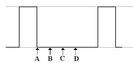
A: The
operation starts.
B: The
inputs to the ALU are stable
C: The
ALU output is stable.
D: The
result is stable in the R1.
The ALU (Arithmetic Logic Unit)
The ALU performs all of the arithmetic and logical
operations for the CPU.
These include the following:
Arithmetic: addition, subtraction, negation, etc.
Logical: AND, OR, NOT, Exclusive OR, etc.
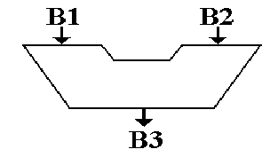
This symbol has been used for the ALU since the mid
1950’s.
It shows two inputs and one output.
The reason for two inputs is the fact that many operations,
such as addition and logical AND, are dyadic;
that is, they take two input arguments.
For
operations with one input, such as logical NOT, one of the input busses will be
ignored and the contents of the other one used.
The Data
Path of a Typical Stored Program Computer
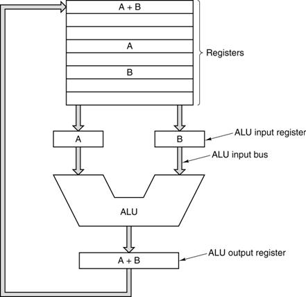
Note the standard way of depicting an ALU. It has two inputs and one output.
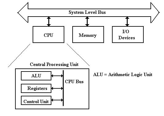
The Central Processing Unit (CPU)
The CPU has four main components:
1. The
Control Unit (along with the IR) interprets the machine language instruction
and issues the control signals to
make the CPU execute it.
2. The
ALU (Arithmetic Logic Unit) that does the arithmetic and logic.
3. The
Register Set (Register File) that stores temporary results related to the
computations. There are also Special Purpose Registers used by the Control Unit.
4. An
internal bus structure for communication.
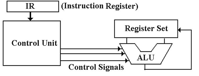
The
function of the control unit is to
decode the binary machine word in the IR (Instruction Register) and issue
appropriate control signals, mostly to the CPU.
Design of the Control Unit
There are two related issues when considering the
design of the control unit:
1) the complexity of the Instruction Set
Architecture, and
2) the microarchitecture used to implement the
control unit.
In order to make decisions on the complexity, we must
place the role of the control unit within the context of what is called the DSI (Dynamic Static Interface).
The ISA (Instruction Set Architecture) of a
computer is the set of assembly language commands that the computer can
execute. It can be seen as the interface
between the software (expressed as assembly language) and the hardware.
A more complex ISA requires a more complex control
unit.
At some point in the development of computers, the
complexity of the control unit became a problem for the designers. In order to simplify the design, the
developers of the control unit for the IBM–360 elected to make it a microprogrammed unit.
This
design strategy, which dates back to the Manchester Mark I in the early 1950’s,
turns the control unit into an extremely primitive computer that interprets the
contents of the IR and issues control signals as appropriate.
The Dynamic–Static Interface
In order to understand the DSI, we must place it
within the context of a compiler for a higher–level language. Although most compilers do not emit assembly
language, we shall find it easier to under the DSI if we pretend that they do.
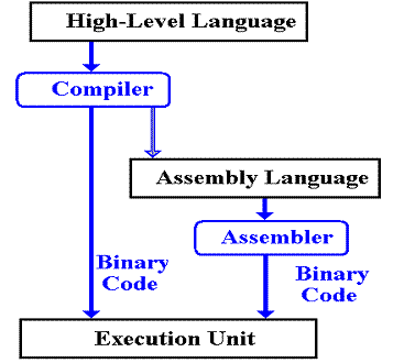
What does the compiler output? There are two options:
1. A very simple assembly language. This requires a sophisticated compiler.
2. A
more complex assembly language. This may
allow a simpler compiler,
but it requires a more complex
control unit.
The Dynamic–Static Interface (Part 2)
The DSI really defines the division between what the
compiler does and what the microarchitecture does. The more complexity assigned to the compiler,
the less that is assigned to the control unit, which can be simpler, faster,
and smaller.
Consider code for the term used in solving quadratic
equations
D = B2 – 4·A·C
In assembly language, this might become
1 LR %R1 A // Load the value into R1
2 LR %R2 B // Load the value into R2
3 LR %R3 C // Load the value into R3
4 MUL %R1, %R3, %R5 // R5 has A·C
5 SHL %R5, 2 //
Shift left by 2 is multiplication by 4
6 MUL %R2, %R2, %R6 // R6 has B2
7 SUB %R6, %R5, %R7 // R7 has B2 – 4·A·C
8 SR %R7 D // Now D = B2 – 4·A·C
Many
of these operations can be performed in parallel. For example, there are no dependencies among
the first three instructions.
Dependency Analysis
The proper sequencing of instructions depends on the
dependencies present.
The following is a dependency graph of this set of 8
assembly language instructions.
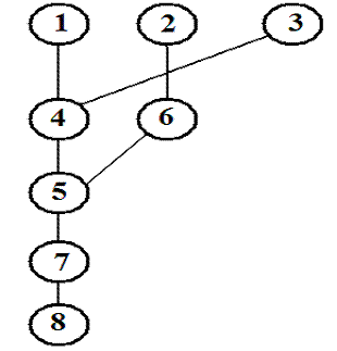
This analysis is much more easily done in software by
the compiler than in hardware by any sort of reasonably simple control unit.
An EPIC Compiler
The compiler for Explicitly Parallel Instruction
Computing is complex.
It might emit the equivalent of the following code.
|
Instruction |
Thread 1 |
Thread 2 |
|
I |
(1) LR %R1 A |
(3) LR %R3 C |
|
II |
(2) LR %R2 B |
(4) MUL %R1, %R3, %R5 |
|
III |
(5) MUL %R2, %R2, %R6 |
(6) SHL %R5, 2 |
|
IV |
(7) SUB %R6, %R5, %R7 |
NOP |
|
V |
(8) SR %R7 D |
NOP |
Again,
the compiler needed some sophisticated analysis to postpone the instruction
“LR %R2 B” to the second instruction slot.
Nevertheless, creating a compiler of such complexity
is much easier that creating a control unit of equivalent complexity.
The Register
File
There are two sets of registers, called “General
Purpose” and “Special Purpose”.
The origin of the register set is simply the need to
have some sort of memory on the computer and the inability to build what we now
call “main memory”.
When reliable technologies, such as magnetic cores,
became available for main memory, the concept of CPU registers was retained.
Registers are now implemented as a set of flip–flops
physically located on the CPU chip.
These are used because access times for registers are two orders of
magnitude faster than access times for main memory: 1 nanosecond vs. 80
nanoseconds.
General
Purpose Registers
These are mostly used to store intermediate results of computation. The count of such registers is often a power
of 2, say 24 = 16 or 25 = 32, because N bits address 2N
items.
The registers are often numbered and named with a
strange notation so that the assembler will not confuse them for variables;
e.g. %R0 … %R15. %R0 is often fixed at
0.
NOTE: It used
to be the case that registers were on the CPU chip and memory was not.
The advent of multi–level
cache memory has erased that distinction.
The Register
File
Special
Purpose Registers
These are often used by the control
unit in its execution of the program.
PC the Program
Counter, so called because it does not count anything.
It is also called the IP (Instruction Pointer), a much better
name.
The
PC points to the memory location of the instruction to be executed next.
IR the Instruction
Register. This holds the machine
language version of
the instruction currently
being executed.
MAR the Memory
Address Register. This holds the
address of the memory word
being referenced. All execution steps begin with PC ® MAR.
MBR the Memory
Buffer Register, also called MDR (Memory Data Register).
This holds the data being
read from memory or written to memory.
PSR the Program
Status Register, often called the PSW (Program Status Word),
contains a collection of
logical bits that characterize the status of the program
execution: the last result
was negative, the last result was zero, etc.
SP on machines that use a stack
architecture, this is the Stack Pointer.
Another
Special Purpose Register: The PSR
The
PSR (Program Status Register) is actually a collection of
bits that describe the running status of the process. The PSR is generally divided into two parts.
ALU Result
Bits: C the carry–out from the last arithmetic
computation.
V set if the last arithmetic operation
resulted in overflow.
N set if the last arithmetic operation gave a
negative number.
Z set it the last arithmetic operation
resulted in a 0.
Control Bits: I set if interrupts are enabled. When I = 1, an I/O device can
raise
an interrupt when it is ready for a data transfer.
Priority A multi–bit field showing the execution
priority of the
CPU;
e.g., a 3–bit field for priorities 0 through 7.
This
facilitates management of I/O devices that have
different
priorities associated with data transfer rates.
Access
Mode The privilege level at which
the current program is
allowed
to execute. All operating systems
require at
least
two modes: Kernel and User.
The CPU Control
of Memory
The
CPU controls memory by asserting control signals.
Within
the CPU the control signals are usually called READ and WRITE.
Reading Memory First place an address in the MAR.
Assert
a READ control signal to command memory to be read.
Wait
for memory to produce the result.
Copy
the contents of the MBR to a register in the CPU.
Writing Memory First place and address in the MAR
Copy
the contents of a register in the CPU to the MBR.
Assert
a WRITE control signal to command the memory.
The
memory control unit might convert these control signals into the Select and R/![]() .
.
In
interleaved memory systems, the memory control unit selects only the addressed
bank of memory. The other banks remain
idle.
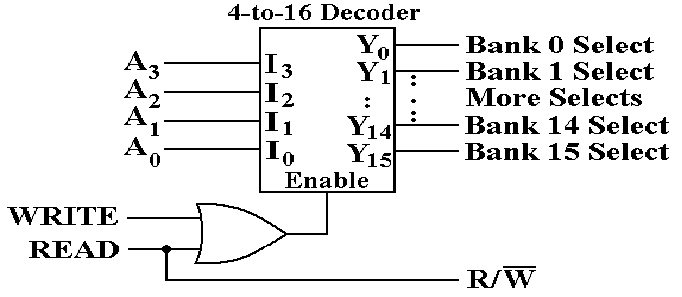
Example: The
CPU Controls a 16–Way Interleaved Memory
Assume
a 64 MB (226 byte) memory with 16 banks that are low–order
interleaved.
The address format might look like the following.
|
Bits |
25 – 4 |
3 – 0 |
|
Use |
Address to the chip |
Bank Select |
Address bits 25 – 4 and
the R/![]() are sent to each of the 16 banks.
are sent to each of the 16 banks.
This shows an
enabled–high decoder used to select the bank when (READ + WRITE) = 1
Input/Output
System
Each I/O device is connected to the system bus through
a number of registers.
Collectively, these form part of the device
interface.
These fall into three classes:
Data Contains data to be written to the
device or just read from it.
Control Allows the CPU to control the
device. For example, the CPU
` might instruct a printer to insert a CR/LF after each line
printed.
Status Allows the CPU to monitor the status
of the device. For example
a printer might
have a bit that is set when it is out of paper.
There are two major strategies for interfacing I/O
devices.
Memory
Mapped I/O is designated
through specific addresses
Load Reg KBD_Data This
would be an input, loading into the register
Store Reg LP_Data This
would be an output, storing into a special address
Isolated I/O
(Instruction–Based I/O) Uses
special instructions.
Input Reg Dev Read
from the designated Input Device into the register.
Output Reg Dev Write
from the register to the designated Output Device
As we shall see, Isolated I/O can also use addresses
for the I/O devices.