Combinational
vs. Sequential Circuits.
Basically,
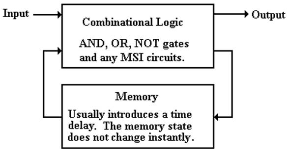
sequential circuits have memory and combinational circuits do not.
Here
is a basic depiction of a sequential circuit.
All
sequential circuits contain combinational logic in addition to the memory
elements.
We
now consider the analysis and design of sequential circuits.
Finite State
Machines: Notation
In
this course, we represent sequential circuits as finite state machines.
A
Finite State Machine (FSM) is a
circuit that can exist in a finite number of states, usually a rather small
number. Finite State Machines with more
than 32 states are rare.
The
FSM has a memory that stores its state.
If
the FSM has N states, then its memory can be implemented with P flip–flops
where
2P–1
< N £ 2P
Typical
values: 3 states 2 flip–flops
4 states 2 flip–flops
5 states 3 flip–flops
8 states 3 flip–flops
Tools
to describe finite states machines include
1) The state diagram
2) The state table
3) The transition table
State
Diagram for a Sequence Detector
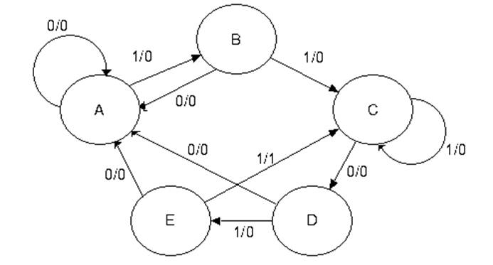
NOTE: We have five states, labeled “A”, “B”, “C”,
“D”, and “E”.
We have labeled edges connecting
the states. Each is labeled Input /
Output.
This is a directed graph with
labeled edges and loops.
More Notes
on the State Diagram
1. The main function of the state diagram for
the FSM is to indicate what the
next state will be given the
present state and input.
2. Here the input is labeled X. Were the input two bits at a time,
the input would be labeled as X1
X0, with X1 the more significant bit.
3. The labeling of the arcs between the states
indicates that there is output
associated with each
transition. Not all Finite State
Machines have
output associated with the
transition. This one does.
4. This and all typical FSM represents a synchronous
machine.
Transitions between states and
production of output (if any) takes place at a fixed
phase of the clock, depending on
the flip–flops used to implement the circuit.
5.
Were we pressed to be more specific,
we would associate the transitions
with the rising edge of the
clock. This is usually an unnecessary
detail.
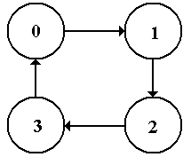
State
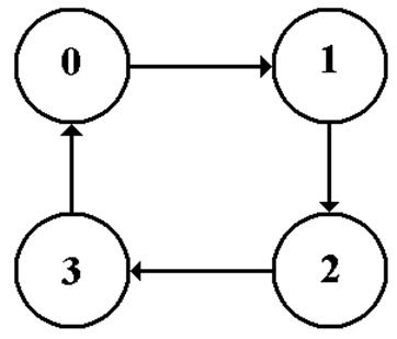
Diagram for a Modulo–4 Counter
Here
is the state diagram for a modulo–4 counter.
There
is no input but the clock. It just
counts clock pulses.
Note
the direction of the arrows; this is an up–counter.
State Tables
The
state table is a tabular form of the state diagram. It is easier to work with.
Here
is the state table for the sequence detector.
|
Present State |
Next State / Output |
|
|
|
X = 0 |
X = 1 |
|
A |
A / 0 |
B / 0 |
|
B |
A / 0 |
C / 0 |
|
C |
D / 0 |
C / 0 |
|
D |
A / 0 |
E / 0 |
|
E |
A / 0 |
C / 1 |
Here is the state table for the
modulo–4 counter.
|
Present State |
Next State |
|
0 |
1 |
|
1 |
2 |
|
2 |
3 |
|
3 |
0 |
Transition
Tables
Transition
tables are just state tables in which the labels have been replaced by binary
numbers. Often the labels are retained
to facilitate translation to binary.
Here
is the transition table for the sequence detector.
|
Present State |
Next State / Output |
|
|
|
X = 0 |
X = 1 |
|
A = 000 |
000 / 0 |
001 / 0 |
|
B = 001 |
000 / 0 |
010 / 0 |
|
C = 010 |
011 / 0 |
010 / 0 |
|
D = 011 |
000 / 0 |
100 / 0 |
|
E = 100 |
000 / 0 |
010 / 1 |
Here is the transition table
for the modulo–4 counter. There is no
output table.
|
Present State |
Next State |
|
0 = 0 0 |
0 1 |
|
1 = 0 1 |
1 0 |
|
2 = 1 0 |
1 1 |
|
3 = 1 1 |
0 0 |
Sample
Circuit for Analysis
The
analysis of such a circuit follows a fixed set of steps.
1) Determine the inputs and outputs of the
circuit. Assign variables to represent
these.
2) Characterize the inputs and outputs of the
flip-flops. Show as Boolean expressions.
3) Construct the Next State and Output Tables.
4) Construct the State Diagram.
5) If possible, identify the circuit. There are no good rules for this step.
Step 1:
Determine the inputs and outputs of the circuit.
The
circuit has one input and one output, with one internal variable of interest.
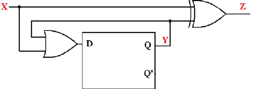
The input is labeled as
X.
The
output is labeled as Z.
The
internal line that is fed back into the flip–flop is labeled as Y.
NOTE: There is output associated with the input because we see the gate
producing
Z based on the input X.
Step 2: Show
the inputs and outputs as Boolean expressions.
Input: X
Output: Z = X Å Y
Input
to Flip–Flop: D = X +Y
Output
of Flip–Flop: Y
Step 3: Construct
the Next State and Output Tables
Here
is the next state table.
|
X |
Q(t) = Y |
D = X + Y |
Q(t+1) |
|
0 |
0 |
0 |
0 |
|
0 |
1 |
1 |
1 |
|
1 |
0 |
1 |
1 |
|
1 |
1 |
1 |
1 |
We know the present
state of the flip–flop; call it Y.
Given
Y and X, the input, we can compute D.
This determines the next state.
Here
is the output table. It depends on the
input and present state.
|
X |
Y = Q(t) |
Z |
|
0 |
0 |
0 |
|
0 |
1 |
1 |
|
1 |
0 |
1 |
|
1 |
1 |
0 |
Step 3A:
Construct the Next State / Output Table
Just
combine the two tables into one table.
|
X |
Q(t) = Y |
D = X + Y |
Q(t+1) / Z |
|
0 |
0 |
0 |
0 / 0 |
|
0 |
1 |
1 |
1 / 1 |
|
1 |
0 |
1 |
1 / 1 |
|
1 |
1 |
1 |
1 / 0 |
We then put the table into a
standard form that will lead to the state diagram.
|
Present State |
Next State/Output |
|
|
|
X = 0 |
X = 1 |
|
0 |
0 / 0 |
1 / 1 |
|
1 |
1 / 1 |
1 / 0 |
We
use this to build a state diagram. The
two states are Q = 0 and Q = 1.
The outputs are associated with the transitions.
Step 4:
Construct the State Diagram.
Here
again is the state table with output.
|
Present State |
Next State/Output |
|
|
|
X = 0 |
X = 1 |
|
0 |
0 / 0 |
1 / 1 |
|
1 |
1 / 1 |
1 / 0 |
Here is the state
diagram.
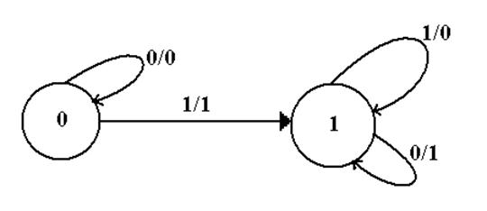
This
is the required answer.
Step 5:
Identify the Circuit if Possible
This
is often hard to do.
The
key here is that the circuit stays in state 0 until the first 1 is input.
When the first 1 is input it goes to state 1 and stays there for all input.
We
now characterize the output as a function of the input for each of the two
states.
Input Q(T) Output
0 0 0 For Q(t)
= 0, the output is X
1 0 1
0 1 1 For Q(t)
= 1, the output is ![]() .
.
1 1 0
It
can be shown that this is a serial generator for a two’s–complement.
The
binary integer is read from Least Significant Bit to Most Significant Bit.
Up
to and including the first (least significant) 1, the input is copied.
After
that it is complemented.
0001
1100 becomes 1110 0100
0010 1101 becomes 1101 0011. Try this, it works.
Design of a
Sequential Circuit
We
begin with the rules for a simple procedure to do the design.
1) Derive
the state diagram and state table for the circuit.
2) Count
the number of states in the state diagram (call it N) and calculate the
number of flip-flops
needed (call it P) by solving the equation
2P–1 < N £ 2P.
This is best solved by guessing the value of P.
3) Assign
a unique P-bit binary number (state vector) to each state.
Often, the first state =
0, the next state = 1, etc.
4) Derive
the state transition table and the output table.
5) Separate
the state transition table into P tables, one for each flip-flop.
WARNING: Things can get
messy here; neatness counts.
6) Decide
on the types of flip-flops to use. When
in doubt, use all JK’s.
7) Derive
the input table for each flip-flop using the excitation tables for the type.
8) Derive
the input equations for each flip-flop based as functions of the input
and current state of all
flip-flops.
9) Summarize
the equations by writing them in one place.
10) Draw
the circuit diagram. Most homework assignments
will not go this far,
as the circuit diagrams
are hard to draw neatly.
Design a
Modulo–4 Counter
Step 1: Derive the state diagram and
state table for the circuit.
Here
is the state diagram. Note that it is
quite simple and involves no input.
Here is the state table for the
modulo–4 counter
|
Present State |
Next State |
|
0 |
1 |
|
1 |
2 |
|
2 |
3 |
|
3 |
0 |
Step 2:
Count the Number of States
Obviously,
there are only four states, numbered 0 through 3.
Determine the number of flip–flops
needed.
Solve
2P–1 < N £ 2P. If N = 4, we
have P = 2 and 21 < 4 £ 22.
We
need two flip–flops for this design.
Number them 1 and 0.
Their
states will be Q1 and Q0 or Y1 and Y0,
depending on the context.
Remember:
21 = 2, 22 = 4, 23 = 8, 24 = 16, 25
= 32, 26 = 64, 27 = 128, etc.
Step 3 Assign a unique P-bit binary number (state
vector)
to each state.
Here
P = 2, so we assign a unique 2–bit number to each state.
For
a number of reasons the first state, state 0, must be assigned Y1 =
0 and Y0 = 0.
For
a counter, there is only one assignment that is not complete nonsense.
|
State |
2-bit Vector |
|
0 |
0 0 |
|
1 |
0 1 |
|
2 |
1 0 |
|
3 |
1 1 |
The 2–bit vectors are
just the unsigned binary equivalent of the decimal state numbers.
Step 4 Derive the state transition table.
|
Present State |
Next State |
|
|
0 |
00 |
01 |
|
1 |
01 |
10 |
|
2 |
10 |
11 |
|
3 |
11 |
00 |
Strictly speaking, we
should have dropped the decimal labels in this step.
However,
this representation is often useful for giving the binary numbers.
The
state transition table tells us what the required next state will be
for each present state.
Step 5 Separate the state transition table into P
tables,
one for each flip-flop.
Here
P = 2, so we need two tables.
|
Flip-Flop 1 |
|
Flip-Flop 0 |
||
|
Present State |
Next State |
|
Present State |
Next State |
|
Y1 Y0 |
Y1( t+1 ) |
|
Y1 Y0 |
Y0( t+1 ) |
|
0 0 |
0 |
|
0 0 |
1 |
|
0 1 |
1 |
|
0 1 |
0 |
|
1 0 |
1 |
|
1 0 |
1 |
|
1 1 |
0 |
|
1 1 |
0 |
Each flip–flop is
represented with the complete present state and its own next state.
Step 6 Decide on the types of flip-flops to use.
When in doubt, use all JK’s.
Our
design will use JK flip–flops.
For
design work, it is important that we remember the excitation table.
Here
it is.
|
Q( t ) |
Q( t+1 ) |
J |
K |
|
0 |
0 |
0 |
d |
|
0 |
1 |
1 |
d |
|
1 |
0 |
d |
1 |
|
1 |
1 |
d |
0 |
Step 7 Derive the input table for each flip-flop using
the excitation tables for the type.
Here
is the table for flip–flop 1.
|
PS |
NS |
Input |
|
|
Y1 Y0 |
Y1 |
J1 |
K1 |
|
0 0 |
0 |
0 |
d |
|
0 1 |
1 |
1 |
d |
|
1 0 |
1 |
d |
0 |
|
1 1 |
0 |
d |
1 |
Here is the table for
flip–flop 0.
|
PS |
NS |
Input |
|
|
Y1 Y0 |
Y0 |
J0 |
K0 |
|
0 0 |
1 |
1 |
d |
|
0 1 |
0 |
d |
1 |
|
1 0 |
1 |
1 |
d |
|
1 1 |
0 |
d |
1 |
Step 8 Derive the input equations for each flip-flop
I
use a set of intuitive rules based on observation and not on formal methods.
1) If a column does not have a 0 in it, match
it to the constant value 1.
If a column does not have a 1 in it,
match it to the constant value 0.
2) If the column has both 0’s and 1’s in it,
try to match it to a single variable,
which must be part of the present
state. Only the 0’s and 1’s in a column
must match the suggested function.
3) If every 0 and 1 in the column is a
mismatch, match to the complement
of a function or a variable in the
present state.
4) If all the above fails, try for simple
combinations of the present state.
NOTE: The use of the complement of a state in step
3 is due to the fact that
each flip–flop outputs
both its state and the complement of its state.
Step 8 Derive the input equations for each flip-flop
Here
is the input table for Flip–Flop 1
|
PS |
NS |
Input |
|
|
Y1 Y0 |
Y1 |
J1 |
K1 |
|
0 0 |
0 |
0 |
d |
|
0 1 |
1 |
1 |
d |
|
1 0 |
1 |
d |
0 |
|
1 1 |
0 |
d |
1 |
J1
= Y0 K1 = Y0
Here is the input table for
Flip–Flop 0
|
PS |
NS |
Input |
|
|
Y1 Y0 |
Y0 |
J0 |
K0 |
|
0 0 |
1 |
1 |
d |
|
0 1 |
0 |
d |
1 |
|
1 0 |
1 |
1 |
d |
|
1 1 |
0 |
d |
1 |
J0
= 1 K0 = 1
Step 9 Summarize the equations by writing them in one
place.
Here
they are.
J1 = Y0 K1
= Y0
J0 = 1 K0 = 1
For
homework and tests, this is required so that I can easily find the answers.
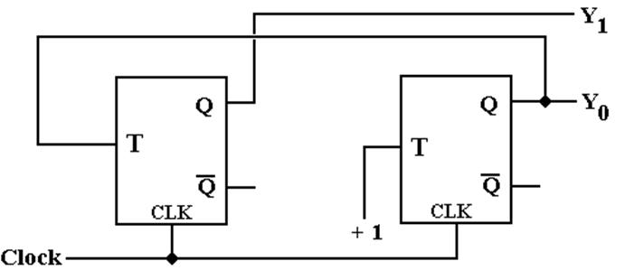
Step 10 Draw the circuit diagram.
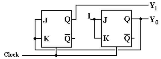
But
note that each flip–flop has input J = K.
This suggests a simplification.
Step 10A Draw the circuit diagram again.
Here
is a simpler version.