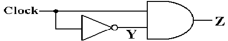
Another
Circuit Dependent on Gate Delay
The
following is a statement of the Inverse Law of Boolean Algebra

But
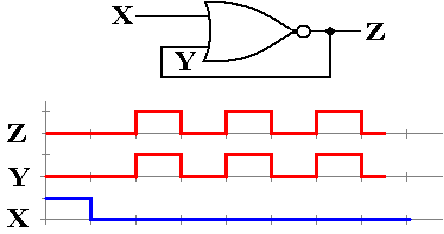
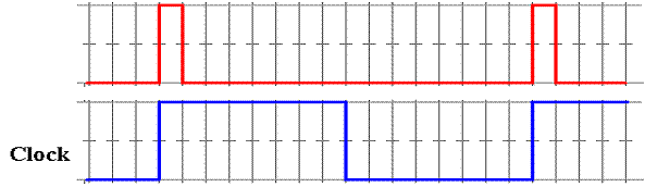
consider the following circuit and its timing diagram
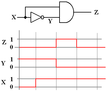
Note
that for a short time (one gate delay) we have Z = 1.
This
is a pulse generator.
A NOR Gate
with Feedback
We
consider yet another circuit that is based on gate delays.
This
is based on the NOR gate, which is an OR gate followed by a NOT gate.

Now
consider the truth table for the NOR gate, which we build from the truth tables
for the OR gate and the NOT gate.
|
X
|
Y
|
W
|
Z
|
|
0
|
0
|
0
|
1
|
|
0
|
1
|
1
|
0
|
|
1
|
0
|
1
|
0
|
|
1
|
1
|
1
|
0
|
The important thing to
note is can be expressed in two equations.
A NOR Gate
with Feedback (Part 2)
Consider
the following circuit. When X = 1, Z =
0, and Y = 0. It is stable.
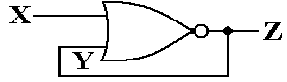
The
behavior becomes interesting when X = 0.
Just after X becomes 0, we still
have Z = 0 and Y = 0 due to gate delays.
But NOR(0, 0) = 1, so after one gate delay,
we have Z = 1 and Y = 1. But NOR(0, 1) =
0, so after another gate delay, we have Z = 0.
This
might be used to generate a system clock, though it probably lacks the stability
and accuracy that are normally expected of such a device.
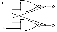
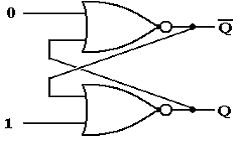
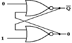
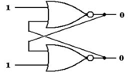
Cross–Coupled
NOR Gates: The SR Latch
Consider
the following circuit. Each of the two
NOR gates has two inputs, one from an external source and one that is fed back
from the other NOR gate.
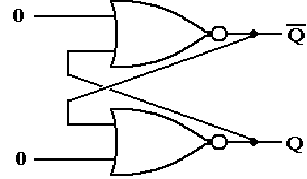
Here
the two external inputs are 0 and 0. We
do not specify the outputs, except to require that one is the complement of the
other; if Q = 1, then  = 0, and vice versa.
The two inputs to the top NOR
gate are 0 and Q. But
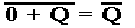
so
this part of the circuit is stable.
The two inputs to the bottom
NOR gate are 0 and . But
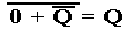
so
this part of the circuit is also stable.
The
circuit is stable with external inputs of 0 and 0.
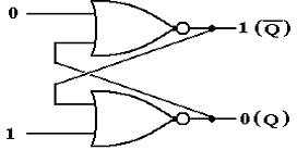
The SR Latch
(Part 2)
Let the above be in either
state (Q = 0 or Q = 1) and change the external input.
At first, the output does not change (remember the gate delays).
After one gate delay, the
output of the top NOR gate changes to 0.
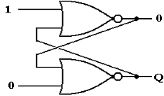
The inputs to the bottom NOR
gate are now 0 and 0. After another gate
delay it changes.
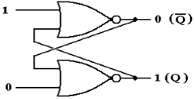
The SR Latch
(Part 3)
Let the above be in either
state (Q = 0 or Q = 1) and change the external input.
At first, the output does not change (remember the gate delays).
After one gate delay, the
output of the bottom NOR gate changes to 0.
The inputs to the top NOR
gate are now 0 and 0; its output changes to 1.
The SR Latch
(Part 4)
We
now have a basic memory device, which stores one bit denoted as Q.
Here is the general circuit diagram of the device.
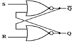
So, we have a device that can
store a single bit, with the following options:
1. Store
a 0
2. Store
a 1
3. Retain
the current contents.
The
behavior of such a memory device is described by its characteristic table.
The SR Latch
(Part 5)
What
about the other input: S = 1 and R = 1.
Remember
that if one input of a NOR gate is logic 1, its output is logic 0.
Specifically for any value of Q, we have:
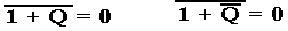
This leads to the circuit
with the following stable state.
But
we cannot have both Q = 0 and = 0.
At
this point, we have two options:
1. Give up on using this device as a
memory device, or
2. Disallow the inputs S = 1 and R =
1. We choose this option.
S = 1 and R = 1 will be labeled as
the next state to be an ERROR.
The SR Characteristic
Tables
Here
is the complete version of the characteristic table. It has eight rows.
|
S
|
R
|
Present State
|
Next State
|
|
0
|
0
|
0
|
0
|
|
0
|
0
|
1
|
1
|
|
0
|
1
|
0
|
0
|
|
0
|
1
|
1
|
0
|
|
1
|
0
|
0
|
1
|
|
1
|
0
|
1
|
1
|
|
1
|
1
|
0
|
ERROR
|
|
1
|
1
|
1
|
ERROR
|
We almost always abbreviate the
above table as follows.
|
S
|
R
|
Next State
|
|
0
|
0
|
Present State
|
|
0
|
1
|
0
|
|
1
|
0
|
1
|
|
1
|
1
|
ERROR
|
The SR
Excitation Tables
Excitation
tables present a slightly different view of flip–flops.
These tables are logically equivalent to the characteristic tables, but
presented differently.
If
the Present State
is 0 and the desired Next
State is 0, we have two
options:
S = 0 and R = 0 This keeps the state the same.
S = 0 and R = 1 This forces the state to 0.
This
is abbreviated as S = 0 and R = d (don’t care), because if the Present State is 0 and
S = 0, the Next State will be 0 without regard to the value of R.
If
the Present State
is 0 and the desired Next
State is 1, we must have
S = 1 and R = 0.
If
the Present State
is 1 and the desired Next
State is 0, we must have
S = 0 and R = 1.
If
the Present State
is 1 and the desired Next
State is 1, we again have
two options:
S = 0 and R = 0 This keeps the state the same.
S = 1 and R = 0 This forces the state to 1. Thus, S = d and R = 0.
Here is the Excitation Table
for an SR Latch.
|
PS
|
NS
|
S
|
R
|
|
0
|
0
|
0
|
d
|
|
0
|
1
|
1
|
0
|
|
1
|
0
|
0
|
1
|
|
1
|
1
|
d
|
0
|
Clocked
Latches and Flip–Flops
Both
latches and flip–flops store a single binary value, often called the “state”.
Latches
of the sort just discussed can lead to unpredictable instabilities. Our goal will be to have a circuit element
with a definite present state, rules
for generating its next state, and
some control over when the device changes state.
The
system clock provides a mechanism by which we may have circuits that meet this
design criterion. These are called “synchronous circuits”.
Both
clocked latches and flip–flops change state only at fixed intervals of a
repeating signal called the system clock.
We now denote the states as follows.
The
present state of the flip–flop is often called Q(t)
The next state of the flip–flop is often called Q(t
+ 1)
The
sequence: the present state is Q(t), the
clock “ticks”, the state is now Q(t + 1)
Denote
the present time by the symbol t. Since our focus is only on how a circuit
element transitions from one state to the next, we do not worry about actual
clock time.
In
other words, the next time period is called t
+ 1, even if it is 0.5 nanoseconds later.
Views of the
System Clock
There
are a number of ways to view the system clock.
In general, the view depends on the detail that we need in discussing
the problem. The logical view is shown
in the next figure, which illustrates some of the terms commonly used for a
clock.
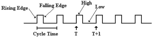
The
cycle time will be denoted by the Greek letter t.
The
clock is typical of a periodic function.
There is a period t for which
f(t) = f(t + t)
This
clock is asymmetric. It is often the case that the clock is symmetric, where the time spent at the
high level is the same as that at the low level. Your instructor often draws the clock as
asymmetric, just to show that such a design is allowed.
Clock Period
and Frequency
If
the clock period is denoted by t, then the frequency (by
definition) is f = 1 / t.
For
example, if t = 2.0 nanoseconds, also written as t = 2.0·10–9 seconds, then
f = 1 / (2.0·10–9 seconds) = 0.50·109 seconds–1 or 500 megahertz.
If
f = 2.5 Gigahertz, also written as
2.5·109 seconds–1,
then
t = 1.0 / (2.5·109 seconds–1) = 0.4·10–9 seconds = 0.4 nanosecond.
Views of the
System Clock
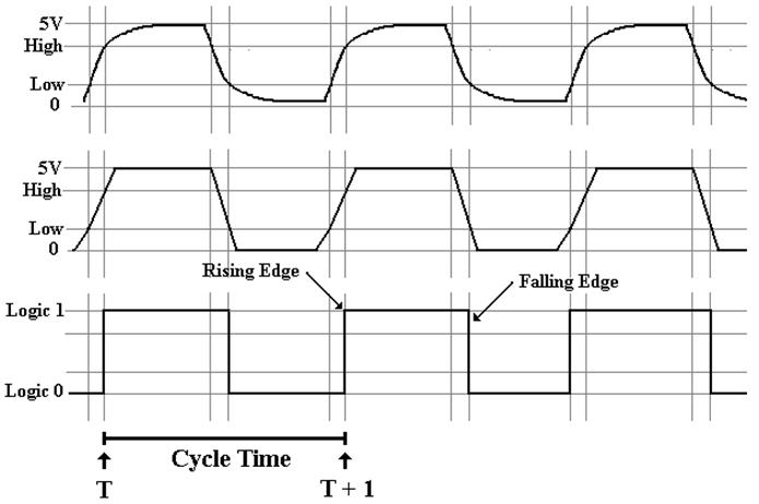
The
top view is the “real physical view”. It
is seldom used.
The middle view reflects the fact that voltage levels do not change instantaneously.
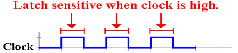
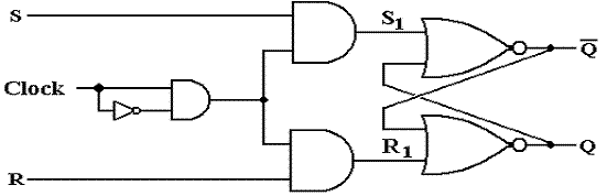
The Clocked
SR Latch
Clocked
latches are sometimes called “level
triggered flip–flops”. These are
sensitive to their input only during one phase of the clock, either when it is
high or it is low.
We
describe a clocked latch that is sensitive to its input only when the clock is
high.
Here is the requirement in terms of the clock.
Here
is the circuit that implements this design criterion.
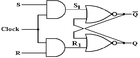
Note
that when Clock = 0, we have S1 = 0 and R1 = 0 without
regard to the values of
S and R. The latch does not change. When Clock = 1, we have S1 = S and
R1 = R.
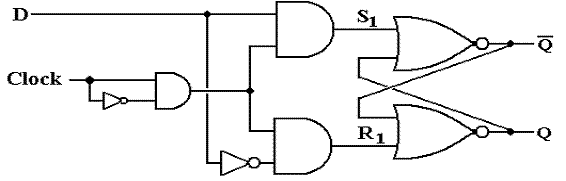
The Clocked
D Latch
We
now introduce a variant of the SR latch that is specialized to store data.
It
is the D Latch, also called the “Data Latch”.
It will store data on every clock pulse.
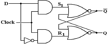
When Clock = 0, then
each of S1 and R1 is 0. No
change in state.
When Clock = 1 and D = 0, then S1 = 0 and R1 = 1. Latch is cleared; Q = 0.
When Clock = 1 and D = 1, then S1 = 1 and R1 = 0. Latch
is set; Q = 1.
The
D Latch and the D Flip–flop (to be defined soon) are quite useful in building
devices that store data. Examples are
registers and I/O interface controls.
The Feedback
Problem
Clocked
latches have one major problem: they are sensitive to input for too long a
time.
Overly
extended sensitivity to input can lead to instabilities.
Consider
the following problem, which is routinely addressed in a computer.
There
is a register called the PC (Program
Counter).
As a regular part of program execution it is incremented: PC ¬ (PC) + 1.
This
operation is so frequently done that every CPU has a dedicated path for it.
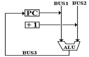
There is a dedicated
constant register permanently set to hold the value 1.
The
ALU adds 1 to the contents of the PC and feeds the result back to the PC.
The Feedback
Problem (Part 2)
Suppose
the Program Counter is implemented as a set of D Latches.
Problems
will occur if the feedback comes at the wrong phase of the clock.
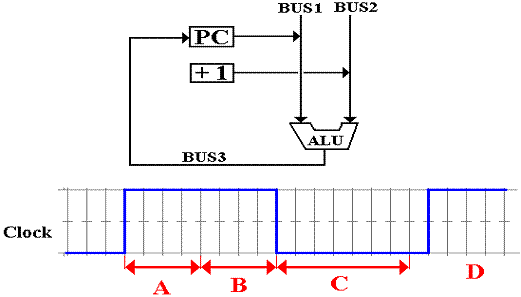
The
addition operation begins just after the rising edge of the clock. If the result of the addition reaches the set
of latches holding the PC too soon, we have problems.
A This
will definitely cause problems. The PC
will be incremented by 2.
B This
might cause problems.
C This
is the best time for the feedback to arrive at the latches.
D The
feedback is too late; the PC is not incremented. This rarely occurs.
The Feedback
Problem (Part 3)
We
need to reduce the time during which the register will accept input.
What
we need is reflected in the following timing diagram.
Suppose
a circuit that causes the latches to be sensitive to input for only one gate
delay.
The
ALU will have at least one gate in its circuitry, as do the modified latches
for the PC.
As
a result, the feedback cannot get
back to the PC while it is still sensitive to input.
Instabilities cannot occur.
We
can modify the latch by adding a pulse generator, discussed previously.
A
latch so modified is called a Flip–Flop.
The SR and D
Flip–Flops
Here
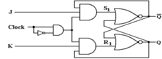
is the circuit diagram for an SR flip–flop that is fabricated from NOR gates.
One can also fabricate it from NAND gates, but we ignore this option.
Here
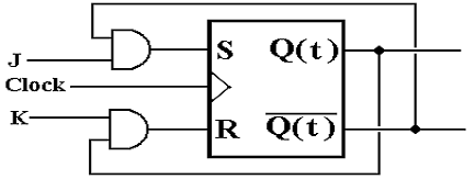
is the circuit diagram for a D flip–flop that is fabricated from NOR gates.
We Need
Another Flip–Flop
Consider
the characteristic table for the SR flip–flop.
It
is the same as that for the SR latch, except for the explicit reference to the
clock.
|
S
|
R
|
Q(t + 1)
|
|
0
|
0
|
Q(t)
|
|
0
|
1
|
0
|
|
1
|
0
|
1
|
|
1
|
1
|
ERROR
|
Were we to modify the SR
flip–flop, what could be placed in the last row?
It
is easy to see that there are only four Boolean functions of a single Boolean
variable Q.
F(Q) = 0, F(Q) = Q, F(Q) =  , and F(Q) = 1. The
above table is missing .
, and F(Q) = 1. The
above table is missing .
This
gives rise to the JK, the most general of the flip–flops. Its characteristic table is:
|
J
|
K
|
Q(t + 1)
|
|
0
|
0
|
Q(t)
|
|
0
|
1
|
0
|
|
1
|
0
|
1
|
|
1
|
1
|

|
The JK
Flip–Flop
One
can modify an SR flip–flop to have the desired characteristics.
It
can be shown that the following circuit does the job.
It
can be shown that the circuit above is logically equivalent to the next one.
The
second circuit slightly facilitates the proof that the JK operates as
advertised.
Design and
Analysis Based on Flip–Flops
We
have shown the detailed construction of flip–flops only to show that they work.
We
now move to issues associated with the use of flip–flops.
For
these issues, we begin to view the devices as “bit boxes” that somehow store
the binary data with the proper timings.
We
focus on two tables for each flip–flop.
The
characteristic table specifies the next state for the present state and input.
The
excitation table specifies the input required to take the flip–flop from the
given present state to the desired
next state.
|
Table Type
|
Given This
|
Determine This
|
|
Characteristic
|
Present State and Input
|
Next State
|
|
Excitation
|
Present State and Desired Next State
|
Input required.
|
We
now proceed with this view of the flip–flop.
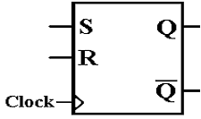
SR Flip–Flop
Here
is the diagram for the SR flip–flop.
Here
again is the state table for the SR flip–flop.
|
S
|
R
|
Q(t + 1)
|
|
0
|
0
|
Q(t)
|
|
0
|
1
|
0
|
|
1
|
0
|
1
|
|
1
|
1
|
Error
|
Here
is the Excitation Table for an SR Flip–Flop.
|
Q(t)
|
Q(t + 1)
|
S
|
R
|
|
0
|
0
|
0
|
d
|
|
0
|
1
|
1
|
0
|
|
1
|
0
|
0
|
1
|
|
1
|
1
|
d
|
0
|
JK Flip–Flop
A
JK flip–flop generalizes the SR to allow for both inputs to be 1.
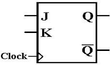
Here
is the characteristic table for a JK flip–flop.
|
J
|
K
|
Q(t + 1)
|
|
0
|
0
|
Q(t)
|
|
0
|
1
|
0
|
|
1
|
0
|
1
|
|
1
|
1
|
|
Here
is the Excitation Table for a JK Flip–Flop.
|
Q(t)
|
Q(t + 1)
|
J
|
K
|
|
0
|
0
|
0
|
d
|
|
0
|
1
|
1
|
d
|
|
1
|
0
|
d
|
1
|
|
1
|
1
|
d
|
0
|
The D
Flip–Flop
The
D flip–flop specializes either the SR or JK to store a single bit. It is very useful for interfacing the CPU to
external devices, where the CPU sends a brief pulse to set the value in the
device and it remains set until the next CPU signal.
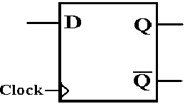
The
characteristic table for the D flip–flop is so simple that it is expressed
better as the equation Q(t + 1) =
D. Here is the table.
The excitation table for
a D flip–flop is usually not given.
It is better represented by an equation D = Q(t
+ 1).
The T
Flip–Flop
The
“toggle” flip–flop allows one to change the value stored. It is often used in circuits in which the
value of the bit changes between 0 and 1, as in a modulo–4 counter in which the
low–order bit goes 0, 1, 0, 1, 0, 1, etc.
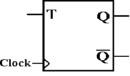
The
characteristic table for the T flip–flop is so simple that it is expressed
better as the equation Q(t + 1) = Q(t) Å T. Here is the
table.
|
T
|
Q(t + 1)
|
|
0
|
Q(t)
|
|
1
|

|
We could give an
excitation table for the T flip–flop, but the idea is better expressed by the
excitation equation.
T = Q(t) Å Q(t + 1)
The JK
Flip–Flop as a General–Use Flip–Flop
The
JK flip–flop can be used to implement any of the other three flip–flops.
As a D flip–flop
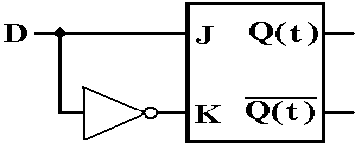
As a T flip–flop
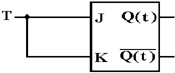
As an SR flip–flop. Just never use
J = 1 and K = 1 as simultaneous inputs.
A Real JK
Flip–Flop
All
real flip–flops have additional inputs.
Here is a more complete diagram.
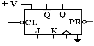
First the flip–flop has a
voltage input (usually 5 volts) and a ground attachment.
All flip–flops are electrical devices that require power and ground.
The
flip–flop has a clock input that enables it to change state. The triangle
indicates that this is an edge–triggered device, a true flip–flop.
As
an edge–triggered device, the flip–flop changes on the rising edge of the
clock.
All flip–flops have asynchronous inputs that can take effect at any time.
Note the circles on these two inputs; they are active low.
CL Clear When
this is set to logic zero, the flip–flop is cleared; Q = 0.
PR Preset When
this is set to logic zero, the flip–flop is set to logic 1; Q = 1.
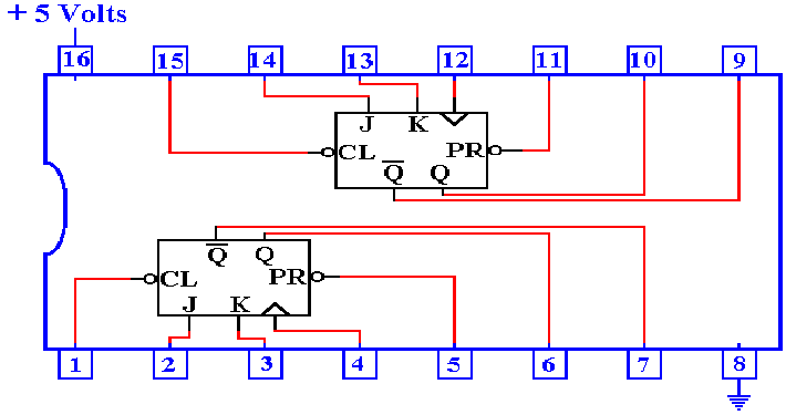
A Real JK
Flip–Flop: The 74LS109A
Here
is the circuit diagram of the 74LS109A, a dual JK flip–flop.
Tri–State to
Attach Flip–Flops to a Bus
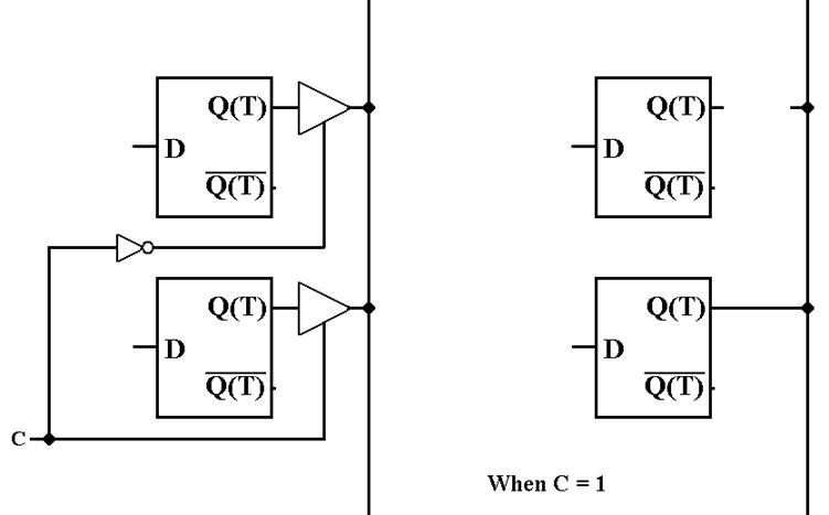
The
control unit must insure that at most one flip–flop is connected to the bus
line.