Design with Multiplexers
Consider
the following design, taken from the 5th edition of my textbook.
This
is a correct implementation of the Carry–Out of a Full Adder.
In terms of Boolean expressions, this is F(X, Y, Z) = S(3, 5, 6, 7).
We
try this with a common circuit emulator, such as Multi-Media Logic,
and find that we need to think about more.
An Eight–to–One MUX in Multi–Media
Here
is the circuit element selected in the Multi–Media Logic tool.
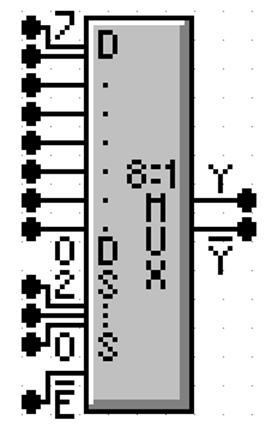
This
is an 8–to–1 MUX with inputs labeled 7 through 0, or equivalently
X7 through X0.
This is expected.
The
selector (control) lines are as expected; 2 through 0.
In
my notes, I use M for the output of the Multiplexer. This figure uses
the symbol Y (not a problem) and notes that real multiplexers
also output the complement.
The
only issue here is the enable. Note that
the MUX is enabled low;
this signal must be set to ground in order for the multiplexer to
function as advertised.
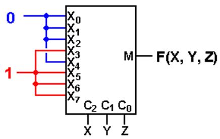
Carry–Out of a Full Adder
Here
is a screen shot of my implementation of F(X, Y, Z) = S(3, 5, 6, 7).
NOTE: Show simulation here.
Gray Codes: Minimal Effort Testing
Consider
the above circuit with three basic inputs S2, S1, S0.
How can one test all possible inputs with minimum switching?
One
good answer is to use Gray Codes for input.
Here are the 2–bit and 3–bit codes.
00 000
01 001
11 011
10 010
110
111
101
100
To
generate an (N + 1)–bit code set from an N–bit code set.
1. Write
out the N–bit codes with 0 as a prefix, then
2. Write
out the N–bit codes in reverse with 1 as a prefix.
00,
01, 11, 10 becomes 000, 001,
011, 010, 110, 111, 101, and 100
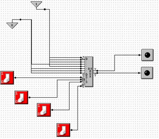
Testing the Carry–Out Circuit
If
the Enable switch is set to 1, the output is always 0. Y’ = 1.
Set
the Enable switch to 0 and generate the following sequence.
Start with S2 = 0, S1 = 0, S0
= 0. 0 0 0
Click S0 to get 0 0 1
Click S1 to get 0 1 1
Click S0 to get 0 1 0
Click S2 to get 1 1 0
Click S0 to get 1 1 1
Click S1 to get 1 0 1
Click S0 to get 1 0 0
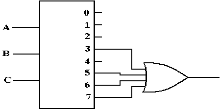
Design with Decoders
We
now look at another circuit from my textbook.
This shows the implementation of a Full Adder with an active high decoder and two OR
gates. The outputs are:
F1 the
Sum
F2 the
Carry–Out
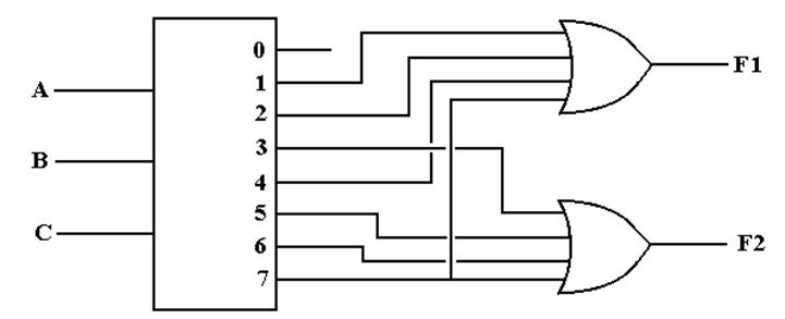
F1(A,
B, C) = S(1, 2, 4, 7) = P(0, 3, 5, 6)
F2(A,
B, C) = S(3, 5, 6, 7) = P(0, 1, 2, 4)
PROBLEM:
Almost all commercial decoders are active
low.
Active Low Decoders
First,
let’s use 3–to–8 decoders to describe the difference between
active high and active low.
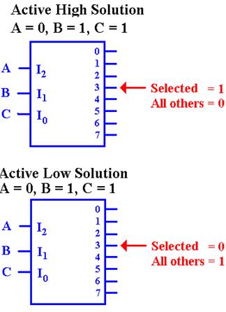
In
the active–high decoder, the active output
is set to +5 volts (logic 1), while the other
outputs are set to 0 volts (logic 0).
In
the active–low decoder, the active output
is set to 0 volts (logic 0), while the other
outputs are set to +5 volts (logic 1).
Enabled Low, Active Low Decoders
All
commercial decoders have an enable input; most are enabled low.
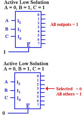
Since
the decoder is enabled low, when the input
signal E’ = 1, none of the decoder outputs are active. Since the
decoder is active low, this means that all of the outputs
are set to logic 1 (+5 volts).
Since
the decoder is enabled low, when the input signal E’ = 0,
the decoder is enabled and the selected output is active. Since the
decoder is active low, this means that the selected output is set to
logic 0, and all other outputs are set to logic 1.
Why Active Low / Enabled Low?
This
is a conjecture, but it makes sense to me.
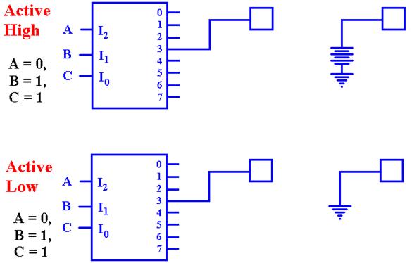
The
active–high decoder is providing power to the device it enables.
The
active–low decoder is just providing a path to ground for the device it
enables.
It is likely that this approach yields a faster circuit.
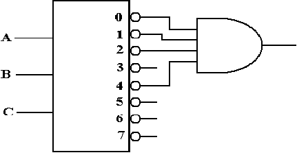
Back To Active High: A Look At F2
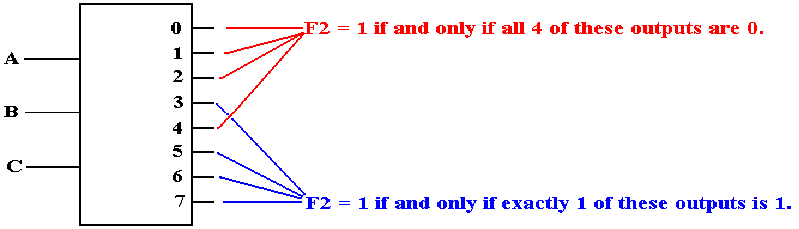
Seeking
a gate that outputs 1 if at least one of its inputs is 1, we are led to the OR
gate.
Active Low: F2(X, Y, Z) = P(0, 1, 2, 4)
F2
is 1 if and only if none of the outputs Y0, Y1, Y2,
or Y4 are selected.
Specifically, each
of those outputs must be a logic 1. This
leads to an AND gate implementation.
Full Adder Implemented with a 3–to–8
Decoder
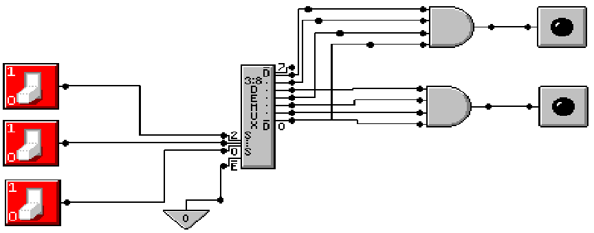
The
sum is at top: F(X, Y, Z) = P(0, 3, 5, 6)
The carry–out is at bottom: F(X, Y, Z)
= P(0, 1, 2, 4)
Where are the Decoders?
One
will note that the Multi–Media Logic tool does not provide a decoder circuit.
Fortunately,
a 1–to–2N demultiplexer can be made into an N–to–2N
decoder.
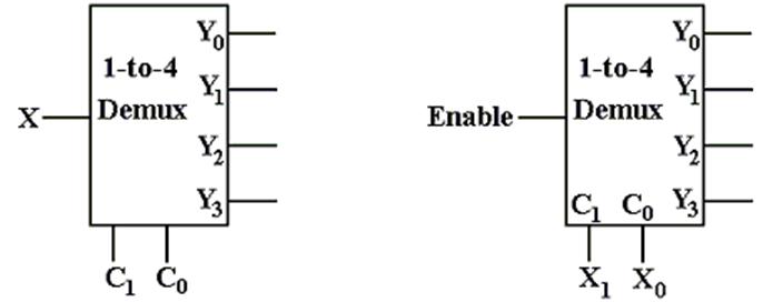
Look
at the circuit to the left. The control
signals C1,C0 select the output to receive the input
X.
This is exactly equivalent to a decoder.
In
the circuit at right, the selected output gets the input, now called “Enable”.
For the demultiplexers we use, the other outputs get a logic 1.
We
can fabricate an active low decoder.
The MUX as
an Active–Low Decoder
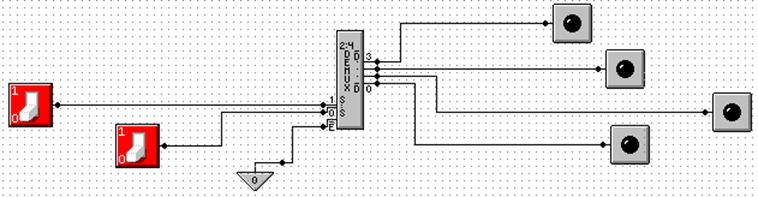
Here
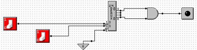
is the 2–to–4 Demultiplexer as an 2–to–4 active low decoder.
Here
is an answer to one of the homework problems: use a 2–to–4 decoder for XOR.
The function is either S(1, 2) or P(0, 3).