The Non–Inverting
Buffer
We
now spend some time investigating useful circuit elements
that do not directly implement Boolean functions.
The
first element is the non–inverting buffer.
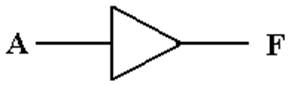
This
is logically equivalent to two NOT gates in a row.
There
are engineering differences between the two, most notably that the
non–inverting buffer delays the signal less than a chain of two NOT gates.
This
is best considered a “voltage adjuster”.
A
logic 1 (voltage in the range 2.0 – 5.0 volts) will be output as 5.0 volts.
A logic 0 (voltage in the range 0.0 – 0.8 volts) will be output as 0.0 volts.
Gate Delays
The
output of a circuit element does not change instantaneously with the input, but
only after a delay time during which the circuit processes the signal.
This
delay interval, called “gate delay”
is about 10 nanoseconds for most simple TTL circuits and about 25 nanoseconds
for TTL Flip–Flops.
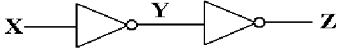
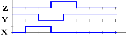
The
simplest example is the NOT gate.
Here
is a trace of the input and output. Note
that the output does not reflect the input until one gate delay after the input
changes.
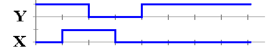
For
one gate delay time we have both X = 1 and Y = 1.
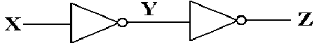
Delay
Circuits
For
some advanced designs, it is desirable to delay a signal by a fixed amount.
One
simple circuit to achieve this effect is based on the Boolean identity.
![]()
A
circuit to implement this delay might appear as follows.
Here
is the time trace of the input and output.
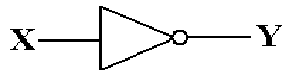
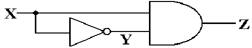
The Pulse
Generator
This
circuit represents one important application of the gate delay principle.
We shall present this circuit now and use it when we develop flip–flops.
This circuit, which I call a “pulse generator”, is based on the
Boolean identity.
![]()
Here is the circuit
Here
is a time plot of the circuit’s behavior.
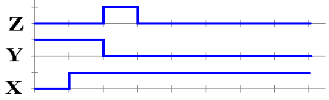
The
pulse is due to the fact that for 1 gate delay, we have both X = 1 and Y = 1.
This is the time it takes the NOT gate to respond to its input and change Y.
The
Tri–State Buffer
Some
time ago, we considered relays as automatic switches.
The tri–state buffer is also an automatic switch.
Here
are the diagrams for two of the four most popular tri–state buffers.
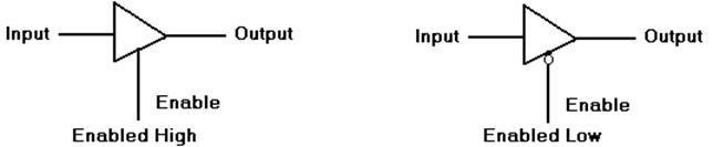
An enabled–low buffer is the
same as an enabled–high buffer with a NOT gate.
What
does a tri–state buffer do when it is enabled?
What does a tri–state buffer do when it is not enabled?
What is this third state implied by the name “tri–state”?
An
Enabled–High Tri–State Buffer
Consider
an enabled–high tri–state buffer, with the enable signal called “C”.
When C = 1, the buffer is enabled.
When C = 0, the buffer is not
enabled.
What
does the buffer do?
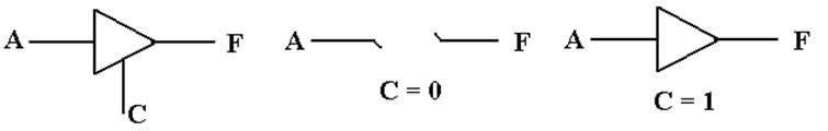
The
buffer should be considered a switch.
When C = 0, there is no connection between the input A
and the output F. When C = 1, the
output F is connected to the input A via what appears to be a non–inverting
buffer.
Strictly
speaking, when C = 0 the output F remains connected to input A, but through a
circuit that offers very high resistance to the flow of electricity. For this reason, the state is often called “high impedance”, “impedance” being an
engineer’s word for “resistance”.
What is This
Third State?
Consider
a light attached to a battery. We
specify the battery as 5 volts,
due only to the fact that this course is focused on TTL circuitry.
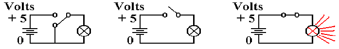
0 volts to lamp Third state 5 volts to lamp
When
the switch is closed and the lamp is connected to the battery, there
is a voltage of +5 volts on one side, 0 volts on the other, and the lamp is on.
In
the case at left, both sides of the lamp are connected to 0 volts.
Obviously, it does nothing.
The
middle diagram shows the third state.
The top part of the lamp is not directly connected to either 0 volts or
5 volts.
In
this third state, the lamp is not illuminated as there is no power to it.
This is similar to the state in which the top is set to 0 volts, but not the
same.
Understanding
Tri–State Buffers
The
best way to understand a tri–state buffer is to consider this circuit.
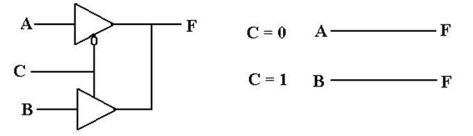
When
C = 0 The
top buffer is outputting the value of A (logic 0 or logic 1)
The bottom
tri–state buffer is not active.
F = A
When
C = 1 The
top tri–state buffer is not active.
The bottom
buffer is outputting the value of B.
F = B
Due
to the arrangement, exactly one tri–state buffer is active at any time.
We
shall use tri–state buffers to attach circuit elements to a common bus,
and trust the control circuitry to activate at most one buffer at a time.