Implementation
of Boolean Logic by Digital Circuits
We
now consider the use of electronic circuits to implement Boolean functions
and arithmetic functions that can be derived from these Boolean functions.
Digital
circuits are built from standard analog components, such as transistors.
It is the manner in which these transistors are used that causes them to
display
the properties required for a digital circuit.
Early
digital circuits were based on electromechanical relays, automatic
switches that were either “on” or “off”.
Relay On Relay Off
In
1937, George Stibitz of Bell Labs developed what he called the “Model K”.
It was a binary full adder based on relays implementing Boolean logic.
He developed the device at home in his kitchen; hence the name.
In 1938, Konrad Zuse
developed a relay–based digital computer, the Z-1, in
his parents’ apartment in Berlin. It was
lost to bombing during the war.
Digital
Technologies
There
are quite a few ways to build digital circuits.
The choice of which to use
in any given device is based on a tradeoff of cost, speed, and power usage.
This
course is based on an older technology that is a bit simpler to understand.
This technology is still seen in digital labs used for teaching.
The
technology is called TTL (Transistor–Transistor Logic). It is based on the
use of transistors in a mode in which they act as switches, much like relays.
Logically,
each TTL device is a Boolean device. All
inputs to this device and
outputs from this device are either logic 0 or logic 1.
Electrically,
these TTL devices are built to a standard that determines how
voltages into the device will be interpreted and what voltage is output.
Here
are the voltage standards for active high TTL, the variety we study.
Input
to Device Output by Device
Logic 1 2.0 to 5.0 volts 2.4 to 5.0 volts
Logic 0 0.0 to 0.8 volts 0.0 to 0.4 volts
Note the greater latitude on input specifications to allow for voltage
degradation.
Basic
Digital Circuit Elements
We
have already discussed these gates, but present them again.
NOT This function takes one
input and produces one output. The gate
is shown
below. The circle at the right end of the triangle
is important.
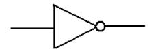
Algebraically,
this function is denoted f(X) = X’ or f(X) = ![]()
The
evaluation of the function is simple: ![]() = 1 and
= 1 and ![]() = 0.
= 0.
Here
is the truth table for the NOT operator.
|
X |
|
|
0 |
1 |
|
1 |
0 |
Basic
Boolean Operators (Part 2)
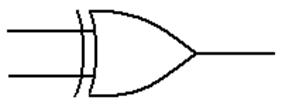
Logic OR
This
is a function of two Boolean variables.
We denote the logical OR of two Boolean
variables X and Y by “X + Y”. Some logic
books will use “X Ú Y”.
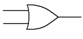
The
evaluation of the logical OR function is shown by a truth table
|
X |
Y |
X + Y |
|
0 |
0 |
0 |
|
0 |
1 |
1 |
|
1 |
0 |
1 |
|
1 |
1 |
1 |
Basic
Boolean Operators (Part 3)
Logic AND
This
is a function of two Boolean variables.
We denote the logical AND of two Boolean
variables X and Y by “X · Y”. Some logic books will use
“X Ù Y”.
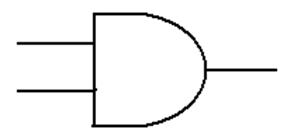
The
evaluation of the logical AND function is shown by a truth table
|
X |
Y |
X · Y |
|
0 |
0 |
0 |
|
0 |
1 |
0 |
|
1 |
0 |
0 |
|
1 |
1 |
1 |
Another
Boolean Operator
While
not a basic Boolean operator, the exclusive OR is very handy.
Logic XOR
This
is a function of two Boolean variables.
We denote the logical XOR of two Boolean
variables X and Y by “X Å Y”. Most logic books seem to
ignore this function.
The
evaluation of the logical XOR function is shown by a truth table
|
X |
Y |
X Å Y |
|
0 |
0 |
0 |
|
0 |
1 |
1 |
|
1 |
0 |
1 |
|
1 |
1 |
0 |
From this last table, we
see immediately that
X Å 0 = X and X Å 1 = ![]()
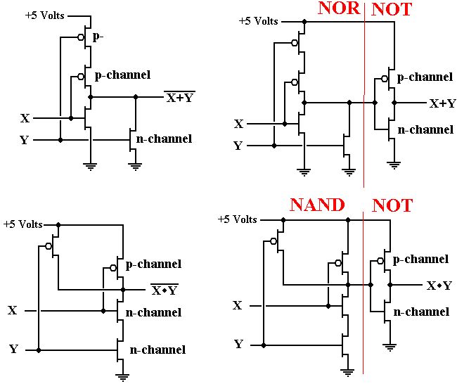
Other Logic
Gates
The
top gate shows the NOR gate and its logical equivalent.
The bottom line shows the NAND gate and its logical equivalent.
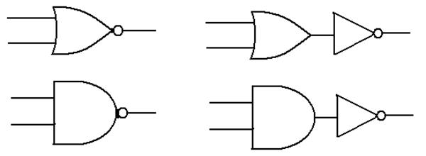
In
my notes, I call these “derived gates” as they are composites of Boolean gates
that are more basic from the purely theoretical approach.
X Y OR NOR X Y AND NAND
0 0 0 1 0 0 0 1
0 1 1 0 0 1 0 1
1 0 1 0 1 0 0 1
1 1 1 0 1 1 1 0
AND Gates
and OR Gates: The Real Way
In
actual fact, the NAND and NOR gates are more primitive than the AND, OR,
and NOT gates in that they are easier to build from transistors.
AND is NOT (NAND)
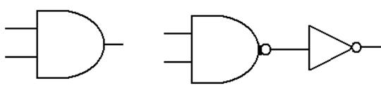 X Y NAND AND
0 0 1 0
0 1 1 0
1 0 1 0
1 1 0 1
OR is NOT (NOR)
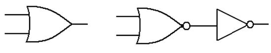 X Y NOR OR
0 0 1 0
0 1 0 1
1 0 0 1
1 1 0 1
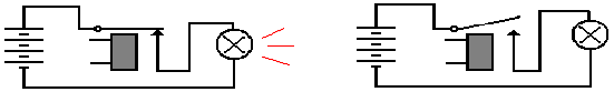
Implementation
of Basic Circuits
These
circuits use simple switches to implement NOT, NOR, and NAND gates.
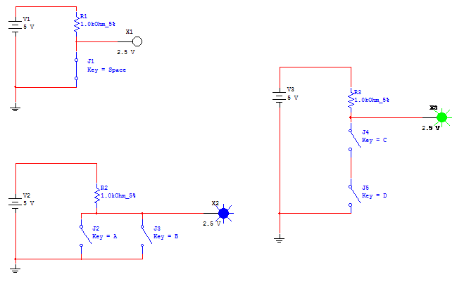
In
the circuit at right, if both switches are closed, (logic 1), the output is 0
volts.
If neither or only one is closed, the output is 5 volts. This is a NAND gate.
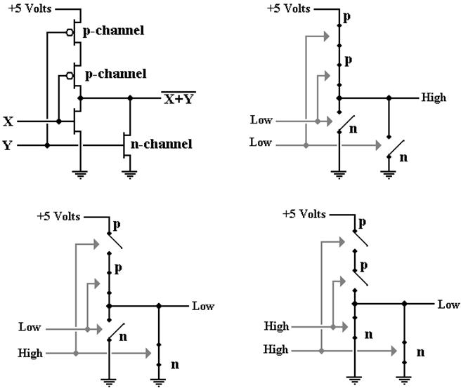
The NOR Gate
Implemented in CMOS
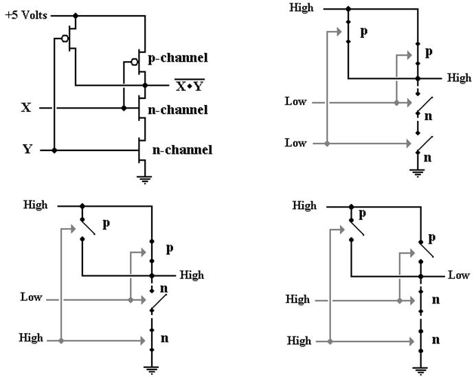
The NAND
Gate Implemented in CMOS
The OR Gate
and the AND Gate
The NAND
Gate as a Universal Gate
We
show how to use a NAND gate to implement the three basic gates of
Boolean logic: AND, OR, and NOT.
We
begin with a simple NAND gate and its truth table.
|
X |
Y |
X·Y |
|
|
0 |
0 |
0 |
1 |
|
0 |
1 |
0 |
1 |
|
1 |
0 |
0 |
1 |
|
1 |
1 |
1 |
0 |
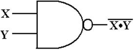
We
now use the NAND gate to implement the basic Boolean devices.
The NAND
Gate as a NOT Gate or an AND Gate
Note
in the above truth table, that if Y = X, then ![]() =
= ![]() =
= ![]() .
.
Here
is the NAND implementation of the NOT gate.
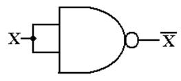
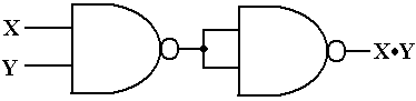
Since
the NAND gate is logically equivalent to NOT (AND), we may use
“double negation” to say that the AND gate is equivalent to NOT (NAND).
Here
is the AND gate as implemented from two NAND gates.
The NAND
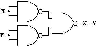
Gate as an OR Gate
In
order to fabricate an OR gate from NAND gates, we must recall
DeMorgan’s laws.
One
of DeMorgan’s laws is usually stated as ![]() =
= ![]() +
+ ![]() .
.
This
can be changed to the form ![]() =
= ![]() +
+ ![]() = X + Y.
= X + Y.
Here
is the circuit.
Multiple–Input
Gates
The
standard definitions of the AND and OR gates call for two inputs.
3–input
and 4–input varieties of these gates are quite common.
Here we give informal, but precise, definitions.
Gate Number of Inputs Output
NOT Exactly 1 0
if input is 1, 1 if input is 0
AND 2 or more 0
if any input is 0
1
if and only if all inputs are 1.
OR 2 or more 1 if any input is 1
0
if and only if all inputs are 0.
NAND 2 or more 1
if any input is 0
0
if and only if all inputs are 1
NOR 2 or more 0
if any input is 1
1
if and only if all inputs are 0.
Example:
“Changing the Number of Inputs”
Some
lab experiments call for gates with input counts other than what we have.
We
begin with two ways to fabricate a 4–input AND gate from 2–input ANDs.
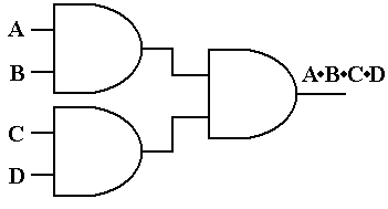
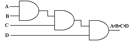
Another
Example
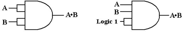
We
now consider how to take a 4–input AND gate and make it act
as if it were a 2–input AND gate.
There
are always multiple solutions. Here are
two solutions.
There are many others.
Fan–Out
By
definition, the fan–out of a logic
gate is the number of other logic
gates receiving input from it.
Considerations
based on electrical engineering limit the fan–out of any gate.
Here
is an OR gate with a fan–out of 5. It
drives five other gates of some kind.
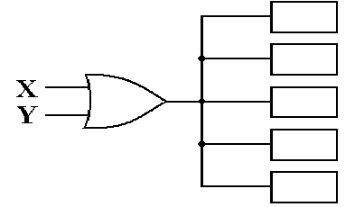
When
the fan–out of a circuit element gets too large, there is a voltage sag.
This
is similar to what can happen in a building when a large motor or
large electric heater turns on.
Controlling
Fan–Out
Upon
occasion, a given large circuit element will have a number of smaller
circuit elements fed from the same input.
There
is a standard design trick to cause that big circuit to present
only one input to the “outside world”.
Here is that trick.
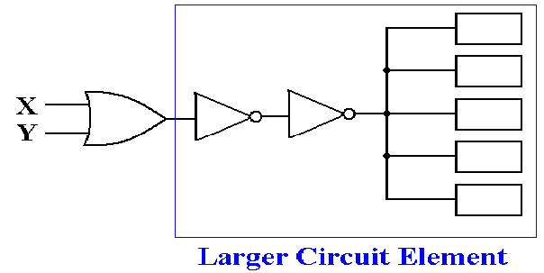
Here
the fan–out issue is transferred to the second NOT gate, which is
internal to the larger circuit element.