Modern
Computers (Circa 2007)
Computing
machines are very common in a modern industrialized society.
The
number of functions performed by these devices is almost endless.
Here is a partial list.
1. General numerical computation, involving both
integers and real numbers.
2. Device automation and control.
3. Message switching, including routers and
firewalls on the Internet.
4. Computer–generated graphics.
5. Graphics–based computer games.
6. Computer–enhanced video.
(How about those extra lines
superimposed on football fields?)
Computers come in two broad classes:
General purpose these are adaptable to a wide
variety of programs.
Special purpose these are designed for one purpose only;
e.g. routers.
Special–purpose computers are usually limited to high
volume markets. It is often easier to
adapt a general–purpose computer to do the job.
General
Purpose Computers
This course will focus on general purpose computers,
also called “Stored Program Computers”
or “Von Neumann Machines”.
In a stored program computer, a program and its
starting data are read into the primary memory of a computer and then
executed. Early computers had no memory
into which programs could be stored.
The first stored program computer designed was the EDVAC, designed by John Von Neumann
(hence the name), John Mauchley, and J. Presper Eckert. The
“Electronic Discrete Variable Automatic Computer” was described in a paper, published on June 30, 1945 with
Von Neumann as the sole author.
The first stored program computer to become
operational was the EDSAC (Electronic Delay Storage Automatic Computer), completed May 6, 1949.
This was developed by Maurice Wilkes of
The first stored program computer that contained all
of the components of a modern computer was the MIT Whirlwind, first demonstrated on April 20, 1951. It was the first to use magnetic core memory.
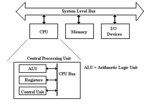
Components
of a Stored Program Computer
The four major components of a modern stored program
computer are:
1. The Central Processing Unit (CPU)
2. The Primary Memory (also called “core memory”
or “main memory”)
3. The Input / Output system
4. One or more system busses to allow the
components to communicate.
Major
Components Defined
The system
memory (of which this computer has 512 MB) is used for transient storage of
programs and data. This is accessed much
like an array, with the memory address
serving the function of an array index.
The Input /
Output system (I/O System) is used for the computer to save data and
programs and for it to accept input data and communicate output data.
Technically the hard drive is an I/O
device.
The Central
Processing Unit (CPU) handles execution of the program.
It has four main components:
1. The
ALU (Arithmetic Logic Unit), which
performs all of the arithmetic
and logical operations of the
CPU, including logic tests for branching.
2. The
Control Unit, which causes the CPU
to follow the instructions
found in the assembly language
program being executed.
3. The
register file, which stores data internally in the CPU. There are user
registers and special purpose
registers used by the Control Unit.
4. A
set of 3 internal busses to allow the CPU units to communicate.
A System Level
Bus, which allows the top–level components to communicate.
Reality
Intrudes (Part 1 of Many)
The design on the previous slide is logically correct,
but IT WON’T WORK.
IT IS TOO SLOW.
Problem: A single system level bus cannot handle the load.
Modern gamers demand fast video; this requires a fast
bus to the video chip.
The memory system is always a performance
bottleneck. We need a dedicated memory
bus in order to allow acceptable performance.
Here is a refinement of the above diagram.
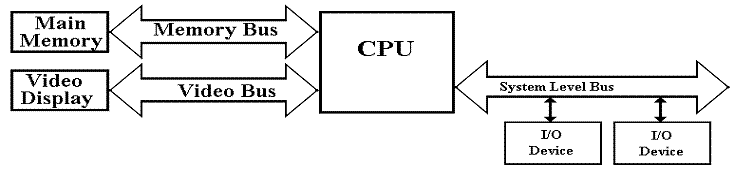
This design is getting closer to reality. At least, it acknowledges two of the devices
requiring high data rates in access to the CPU.
Reality
Intrudes (Part 2 of Many)
We now turn to commercial realities, specifically legacy I/O devices.
When upgrading a computer, most users do not want to
buy all new I/O devices (expensive) to replace older devices that still
function well.
The I/O system must provide a number of busses of
different speeds, addressing capabilities, and data widths, to accommodate this
variety of I/O devices.
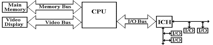
Here we show the main I/O bus connecting the CPU to
the I/O Control Hub (ICH), which is
connected to two I/O busses:
one for slower (older) devices
one for faster (newer) devices.
The Memory
Component
The memory stores the instructions and data for an
executing program.
Memory is characterized by the smallest addressable
unit:
Byte
addressable the smallest unit is
an 8–bit byte.
Word
addressable the smallest unit is a
word, usually 16 or 32 bits in length.
Most modern computers are byte addressable,
facilitating access to character data.
Logically, computer memory should be considered as an
array.
The index into this array is called the address
or “memory address”.
A logical view of such a byte addressable memory might
be written in code as:
Const MemSize =
byte Memory[MemSize] // Indexed
0 … (MemSize – 1)
The CPU has two registers dedicated to handling
memory.
The MAR (Memory Address Register) holds the
address being accessed.
The MBR (Memory Buffer Register) holds the data being written to the
memory or
being read from the memory. This is
sometimes
called the
Memory Data Register.
The
Simplistic Physical View of Memory
I call this the “linear view”, as memory is still
modeled as one large linear array.
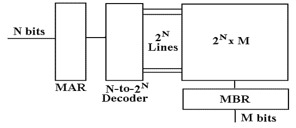
The N–bit address selects one of the 2N
entities, numbered 0 through (2N – 1).
Read sequence: First address to MAR; command a READ.
then copy
the contents of the MBR.
Write sequence: First address to MAR; data to the MBR.
then command
a WRITE.
This is logically correct, but difficult to implement
at an acceptable price.
Multi–Level
Memory
What we want is a very large memory, in which each
memory element is fabricated from very fast components. But fast means expensive.
What we can afford is a very large memory, in which
each memory element is fabricated from moderately fast, but inexpensive,
components.
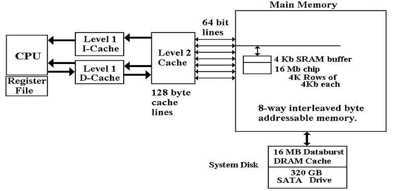
Modern computers achieve good performance from a
large, moderately fast, main memory by using two levels of cache memories, called L1 and L2.
These work due to an observed property of programs, called the locality principle.
A typical arrangement would have a large L2 cache and
a split L1 cache. The L1 cache has an
Instruction Cache and a Data Cache.
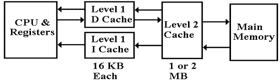
Note that the Instruction Cache (I Cache) does not
write back to the L2 cache.
Organization
of Primary Memory
We turn our attention again to the primary
memory. When we left it, we had a linear
view with an N–to–2N decoder.
We shall study decoders in a later class. At present, it should be obvious that
construction of a 32–to–4,294,967,296 decoder would be very difficult.
Memory on all modern computers is obviously built from
smaller chips. Each of these chips will
be constructed from a number of smaller chips.
For example, a 1 GB memory might have four 256 MB
memory modules.
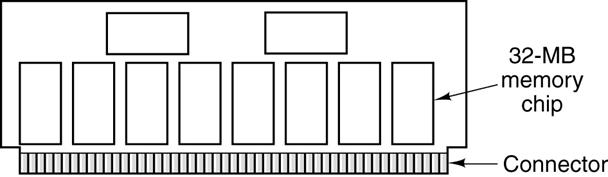
Each 32 MB chip would be organized as eight 32 Mb
chips.
Each 32 Mb chip is organized as an 8,192–by–4,096
array.
Primary
Memory
Also called “core memory”, “store”, or “storage”.
Beginning
with the MIT Whirlwind and continuing for about 30 years, the
basic technology for primary memory involved “cores” of magnetic material.
Virtual
Memory
All modern computer systems use virtual memory. At various
times in the course, we shall give a precise definition, but here is the common
setup.
In
MS–Windows, the area of the system disk that handles virtual memory is called
the paging file. My system has a 768 MB paging file.
The Central
Processing Unit (CPU)
Traditionally, the CPU is considered as having four
main components.
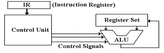
1. The Arithmetic Logic Unit
2. The
three bus structure that feeds the ALU and accepts its results.
3. The
control unit that interprets the machine language.
4. The
register set, containing both general purpose (user) registers, and
special purpose registers. The latter include:
MAR the Memory Address Register.
MBR the Memory Buffer Register.
PC the Program Counter, pointing to the next instruction.
IR the Instruction Register, holding the current instruction.
Memory
Creeps onto the CPU Chip
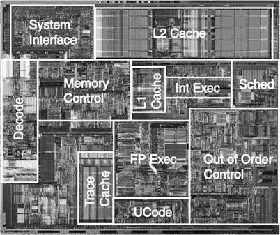
Modern computers, such as the P4, have placed both L1 caches
and the L2 cache on the CPU chip itself.
Here is a picture of the P4 chip, annotated by Intel.
In older computers, the main difference between CPU
registers and memory was that the registers were on the chip and memory was
not. This no longer holds.
Memory on
the CPU Chip (Part 2)
With two L1 caches (the I
cache and the D cache) and the L2 cache on the CPU chip, we look for another
difference to distinguish user registers from memory.
The main difference is historical. It has to do with the way that the assembly
language program accesses the device.
There are register–specific instructions and
memory–specific instructions.
A modern computer (Pentium series excepted) will have
between 8 and 32 user registers. These
store temporary results for computations.
The Pentium register set (EAX, EBX, ECX, and EDX) is
rather unusual and would be cheerfully ignored were the Pentium not such an
important design.
Modern computer architecture usually involves a series
of design tradeoffs.
Question: Should we
place more general–purpose registers on the CPU
chip or have a larger
L1 Data Cache?
Answer: Each
provides about the same improvement in performance.
Flip a coin or use
some other criterion.
The ALU
(Arithmetic Logic Unit)
The ALU performs all of the arithmetic and logical
operations for the CPU.
These include the following:
Arithmetic: addition, subtraction, negation, etc.
Logical: AND, OR, NOT, Exclusive OR, etc.
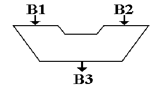
This symbol has been used for the ALU since the mid 1950’s.
It shows to inputs and one output.
The reason for two inputs is the fact that many
operations, such as addition and logical AND, are dyadic; that is, they take two input arguments.
Historical
Summary
Reflecting on the last 60 years of the history of
computing machines, we see a development constrained by the available
technology and economics.
We see a constant move towards devices with
less cost and physical size
more performance and reliability
(longer time between failures).
As an example, the ENIAC seldom functioned for more
than a few hours continuously before it suffered a failure.
Memory technology is a good example. We have four stages.
1. No
memory (ENIAC).
2. Very
unreliable memory, such as mercury delay lines and Williams tubes.
3. Very
reliable memory, specifically magnetic core memory.
4. Very
reliable and inexpensive memory, specifically solid state devices.
We now begin a look at the computer from a logical
view.
The
Fetch–Execute Cycle
This cycle is the logical basis of all stored program computers.
Instructions are stored in memory as machine language.
Instructions are fetched
from memory and then executed.
The common fetch cycle can be expressed in the
following control sequence.
MAR ¬
PC. // The PC contains
the address of the instruction.
READ. // Put the address into the
MAR and read memory.
IR ¬
MBR. // Place the
instruction into the MBR.
This cycle is described in many different ways, most
of which serve to highlight additional steps required to execute the instruction. Examples of additional steps are: Decode the
Instruction, Fetch the Arguments, Store the Result, etc.
A stored program computer is often called a “von
Neumann Machine” after one of the originators of the EDVAC.
This Fetch–Execute cycle is often called the “von Neumann bottleneck”, as the
necessity for fetching every instruction from memory slows the computer.
Avoiding the
Bottleneck
In the simple stored program machine, the following
loop is executed.
Fetch
the next instruction
Loop Until Stop
Execute
the instruction
Fetch
the next instruction
End
The first attempt to break out of this endless cycle
was “instruction prefetch”;
fetch the next instruction at the same time the current one is executing.
As we can easily see, this concept can be extended.
Instruction–Level Parallelism: Instruction Prefetch
Break
up the fetch–execute cycle and do the two in parallel.
This
dates to the IBM Stretch (1959)
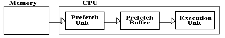
The
prefetch buffer is implemented in the CPU with on–chip registers.
The
prefetch buffer is implemented as a single register or a queue.
The CDC–6600 buffer had a queue of length 8 (I think).
Think
of the prefetch buffer as containing the IR (Instruction Register)
When
the execution of one instruction completes, the next one is already
in the buffer and does not need to be fetched.
Any
program branch (loop structure, conditional branch, etc.) will invalidate the
contents of the prefetch buffer, which must be reloaded.
Instruction–Level
Parallelism: Pipelining
Better
considered as an “assembly line”
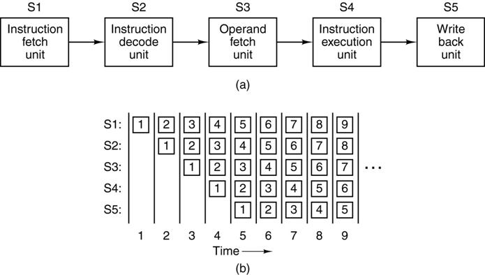
Note
that the throughput is distinct from the time required for the execution of a
single instruction. Here the throughput
is five times the single instruction rate.
What About
Two Pipelines?
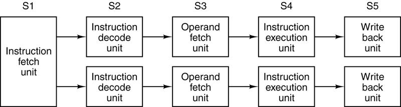
Code
emitted by a compiler tailored for this architecture has the possibility to run
twice as fast as code emitted by a generic compiler.
Some
pairs of instructions are not candidates for dual pipelining.
C = A + B
D = A · C // Need the
new value of C here
This is called a RAW (Read After
Write) dependency, in that the value
for
C must be written to a register before it can be read for the next operation.
Stopping the pipeline for a needed value is called stalling.
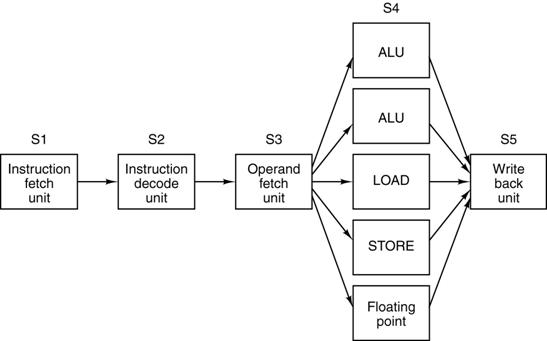
Superscalar
Architectures
Having
2, 4, or 8 completely independent pipelines on a CPU is very
resource–intensive and not directly in response to careful analysis.
Often,
the execution units are the slowest units by a large margin. It
is usually a better use of resources to replicate the execution units.
What Is
Executed? The Idea of Multilevel Machines.
In discussing the fetch–execute cycle, we claimed that
each instruction is fetched and executed.
We now ask about the type of instruction.
In order to answer this question more precisely, we
introduce the idea of a multilevel machine and multiple levels of computer
languages.
We begin this discussion by discussing three levels of
languages.
High–Level Language English–like
statements Z = X + Y
Assembly Language Mnemonic
codes Load X
Add Y
Store
Z
Machine Language Binary
numbers 0x1100
(Here
shown in 0x3101
hexadecimal
form) 0x2102
The machine language used in this example is the MARIE
design (CPSC 2105)
The
Multilevel Machine
Following Andrew Tanenbaum(1),
we define a four–level machine.
Each level of the machine corresponds to a language level.
Machine Language Language Type
M3 L3 High level language such as C++ or Java
M2 L2 Assembly language
M1 L1 Binary machine language
M0 Control Signals Microarchitecture level
Following Tanenbaum, we define a virtual machine as a hypothetical computer that directly executes
language at its level. For example, M3
as a virtual machine directly executes high level language programs.
The student should be aware that there is another,
very important, use of the term virtual machine, with an entirely different
definition. We use that later.
(1) Structured
Computer Organization (5th Edition) by Andrew S. Tanenbaum.
ISBN 0 – 13 –
148521 – 0. Dr. Tanenbaum defines
six levels.
Options for
Executing a High Level Language Program
There are three options for executing a L3
program. Each has been tried.
Direct
Execution. This has been tried with the
This is
much less flexible than the other two approaches,
much
more difficult to implement, and less efficient.
Translation Translate
the L3 program to a lower level language, such
as L2 or
L1. The lower level languages are much
more
based on
the computer hardware, and easier to execute.
For a
HLL, this step is called compilation.
Interpretation Write a
program in a lower level language, either L2 or
L1, that takes the L3 program as input data and causes
the
computer to achieve the desired effect.
Example: The
JVM (Java Virtual Machine) is a virtual machine that
appears
to execute the Java program directly. In
actual
fact, it
translates the Java code into byte code and
interprets
that byte code.
Levels from
the “Bottom Up”
The lowest levels of the computer were not shown on
the above diagram. These are the digital logic level and the analog
devices upon which the level is based.
The microarchitecture
level, the first real level, shows all of the components of the CPU (ALU, Control
Unit, internal busses, user registers, control registers), the set of control signals, as well as the method
of generating these signals.
At this level, the registers are connected to the ALU
to form a data path, over which the
data flow: registers to ALU, then ALU back to a register.
At this level, the basic design question is how to
build the control unit.
The ISA
(Instruction Set Architecture), the next level up, describes the binary
machine language instructions, their mnemonic representations, and the general
purpose registers that can be accessed by a machine language program.
The Higher
Level Language level, the top level, represents the view of the Instruction
Set Architecture as seen through the compiler or interpreter for the higher
level language.
How Does the
Control Unit Work?
The binary form of the instruction is now in the IR (Instruction Register).
The control unit decodes that instruction and
generates the control signals necessary for the CPU to act as directed by the
machine language instruction.
The two major design categories here are hard–wired and microprogrammed.
Hardwired: The control signals are
generated as an output of a
set
of basic logic gates, the input of which derives
from
the binary bits in the Instruction Register.
Microprogrammed: The control signals are generated by a microprogram
that
is stored in Control Read Only Memory.
The
microcontroller fetches a control
word from the
CROM and places it into the mMBR, from which
control
signals are emitted.
The microcontroller can almost be seen as a very
simple computer within a more complex computer.
This simplicity was part of the original motivation.
How to
Handle Complexity in a HLL
Modern computer design practice is driven by the fact
that almost all programs, including Operating Systems, are written in a HLL (High Level Language).
For interpreted programs, the interpreter itself is written in a HLL.
Almost everything executing on a modern computer is
thus the output of a compiler. We now
adjust the ISA to handle compiler output.
But where do we put the complexity associated with
processing a modern HLL?
We could have a straightforward compiler that emitted
complex machine language instructions for execution at the microarchitecture
level. This approach requires a very
sophisticated control unit, which is hard to design.
We could have a very complex compiler (still easy to
write) that emitted more machine language instructions, each of which was very
simple. This approach allows a very
simple control unit, which is easy to design and test.
A hard–wired control unit for the complex ISA of the
first approach was found to be very difficult to design and test. For that reason, a simpler micro–control unit
was designed and microprogrammed.
Modern
Design Realities
Some assumptions that drive current design practice
include:
1. The fact that most programs are written in
high–level compiled languages.
2. The fact that all modern compilers are
designed to emit fairly simple
machine language instructions,
assuming a simple ISA.
3. The fact that a simpler instruction set
implies a smaller control unit,
thus freeing chip area for more
registers and on–chip cache.
4. The fact that current CPU clock cycle times
(0.25 – 0.50 nanoseconds)
are much faster than memory
devices, either cache or primary memory.
5. The considerable experience in writing
sophisticated compilers that can
handle very complex constructs
and emit very efficient machine code.
NOTE: The appearance of a new memory technology with
significantly
enhanced performance would
require a completely new design
approach. This would be welcome, but quite a challenge.
Modern
Design Principles
1. Implement the microarchitecture level to
provide direct hardware execution
of the more common instructions
with micro–routines for the more complex
instructions. Fortunately, the more complex instructions
are rare.
2. Use pipelining and maximize the rate at
which instructions are issued.
3. Minimize the number of instruction formats
and make them simpler, so that
the instructions are more easily
and quickly decoded by the control unit.
4. Provide plenty of registers and the largest
possible on–chip cache memory.
A large number of registers helps
the compiler generate efficient code.
5. Minimize the number of instructions that
reference memory. Preferred
practice is called “Load/Store” in
which the only operations to reference
primary memory are: register loads from memory
register stores into memory.
This implies that many operations, such
as addition and logical AND,
operate only on the contents of CPU
general–purpose registers.