Linear Speedup
Consider a
computing system with N processors, possibly independent. Let C(N) be the cost
of the N–processor system, with C1 = C(1) being the cost of one
processor. Normally, we assume that C(N) » N·C1, that the cost of
the system scales up approximately as fast as the number of processors. Let P(N) be the
performance of the N–processor system, measured in some conventional measure
such as MFLOPS (Million Floating Operations Per Second), MIPS (Million
Instructions per Second), or some similar terms.
Let P1
= P(1) be the performance of a single processor system
on the same measure. The goal of any parallel processor system is linear
speedup: P(N) »
N·P1. More properly, the actual goal is [P(N)/P1] »
[C(N)/C1]. Define the speedup factor as S(N)
= [P(N)/P1]. The goal is S(N) » N.
Recall the
pessimistic estimates from the early days of the supercomputer era that for
large values we have S(N) < [N / log2(N)],
which is not an encouraging number.
|
N
|
100
|
1000
|
10,000
|
100,000
|
1,000,000
|
|
Maximum S(N)
|
15
|
100
|
753
|
6,021
|
30,172
|
It may be that it was these values that slowed the
development of parallel processors. This
is certainly one of the factors that lead Seymour Cray to make his joke
comparing two strong oxen to 1,024 chickens (see the previous chapter for the
quote).
The goal of parallel
execution system design is called
“linear speedup”, in which the performance of an N–processor system is
approximately N times that of a single processor system. Fortunately, there are many problem types
amenable to algorithms that can be caused to exhibit nearly linear speedup.
Linear Speedup: The View from the Early
1990’s
Here is what
Harold Stone [R109] said in his textbook.
The first thing to note is that he uses the term “peak performance” for
what we call “linear speedup”. His
definition of peak performance is quite specific. I quote it here.
“When a
multiprocessor is operating at peak performance, all processors are engaged in
useful work. No processor is idle, and
no processor is executing an instruction that would not be executed if the same
algorithm were executing on a single processor.
In this state of peak performance, all N processors are contributing to
effective performance, and the processing rate is increased by a factor of
N. Peak performance is a very special
state that
is rarely achievable.” [R109].
Stone
notes a number of factors that introduce inefficiencies and inhibit peak
performance.
1. The delays introduced by inter–processor
communication.
2. The overhead in synchronizing the work
of one processor with another.
3. The possibility that one or more
processors will run out of tasks and do nothing.
4. The process cost of controlling the
system and scheduling the tasks.
Motivations for Multiprocessing
Recalling the
history of the late 1980’s and early 1990’s, we note that originally there was
little enthusiasm for multiprocessing. At
that time, it was thought that the upper limit on processor count in a serious
computer would be either 8 or 16. This
was a result of reflections on Amdahl’s Law, to be discussed in the next
section of this chapter.
In the 1990’s,
experiments at Los Alamos and Sandia showed the feasibility of multiprocessor
systems with a few thousand commodity CPUs.
As of early 2010, the champion processor was the Jaguar, a Cray
XT5. It had a peak performance of 2.5
petaflops (2.5·1015
floating point operations per second) and a sustained performance in excess of
1.0 petaflop. As of mid–2011, the Jaguar
is no longer the champion.
Multiprocessing
is designed and intended to facilitate parallel processing. Remember that there are several classes of parallelism,
only one of which presents a significant challenge to the computer system
designer. Job–level parallelism or process–level
parallelism uses multiple processors to run multiple independent programs
simultaneously. As these programs do not
communicate with each other, the design of systems to support this class
of programs presents very little challenge.
The true
challenge arises with what might be called a parallel processing program, in which a single program executes on
multiple processors. In this definition
is the assumption that there must be some interdependencies between the
multiple execution units. In this set of
lectures, we shall focus on designs for efficient execution of solutions to
large single software problems, such as weather forecasting, fluid flow modeling,
and so on.
Most of the rest
of this chapter will focus on what might be called “true parallel processing.”
Amdahl’s Law
Here is a
variant of Amdahl’s Law that addresses the speedup due to N processors.
Let T(N) be the time to execute the program on N processors,
with
T1 = T(1) be the time to execute the program on 1 processor.
The speedup
factor is obviously S(N) = T(1) / T(N). We consider any program as having two
distinct components: the code that can
be sped up by parallel processing, and the code that is essentially
serialized. Assume that the fraction of
the code that can be sped up is denoted by variable X. The time to execute the
code on a single processor can be written as follows: T(1) = X·T1 + (1 – X)·T1 = T1
Amdahl’s Law
states that the time on an N–processor system will be
T(N)
= (X·T1)/N
+ (1 – X)·T1 =
[(X/N) + (1 – X)]·T1
The speedup is S(N) = T(1) / T(N) = 1 / [(X / N) + (1 – X)]
It is easy to
show that S(N) = N if and only if X = 1.0; there is no
part of the code that is essentially sequential in nature and cannot be run in
parallel. Let’s examine the two most
interesting cases. Suppose that X =
1. Then S(N) =
1 / [ 1/N + 0] = 1 / [1/N] = N. Suppose
that X = 0.0, then S(N) = 1 / [0/N + 1] = 1/1 = 1; no
speedup.
Suppose that 0.0
< X < 1.0. Then [(X / N) + (1 –
X)] > (1 – X) and 1 / [(X / N) + (1 – X)] is less than 1 / (1 – X). So we have the maximum speedup for 0.0 < X
< 1.0; it is 1 / (1 – X).
Some Results Due to Amdahl’s Law
Here are some
results on speedup as a function of number of processors.
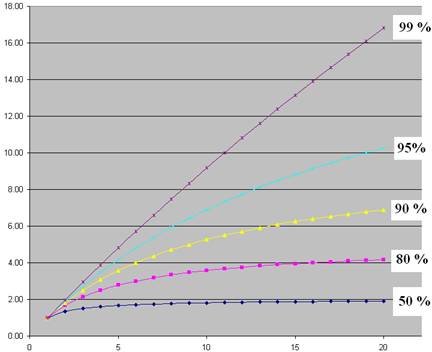
Note that even
5% purely sequential code really slows things down. For much larger processor counts, the results
are about the same.
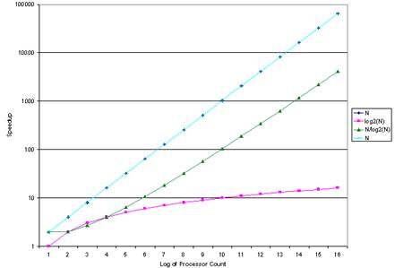
In the 1980’s
and early 1990’s, the N/log2(N) was thought
to be the most likely speedup , with log2(N) a second
candidate. Each of these was
discouraging. For N/log2(N) speedup, S(1024)
= 102 and S(65536) = 4096. For log2(N) speedup, S(1024) = 10 and S(65536) = 16. Who would want to pay 65,536 times the
dollars for 16 times the performance?
Flynn’s Taxonomy
Taxonomy is just
a way of organizing items that are to be studied. Here is the taxonomy of computer designs developed
by Michael Flynn, who published it in 1966.
|
|
|
Data
Streams
|
|
|
|
Single
|
Multiple
|
|
Instruction
Streams
|
Single
|
SISD
(Standard computer)
|
SIMD
(SSE on x86)
|
|
Multiple
|
MISD
(No examples)
|
MIMD
(Parallel processing)
|
The classification focuses on two of the more
characterizations of processing: the nature of the data streams and the number
of processors applied to those data streams.
The simplest, of course, is the SISD
design, which characterizes most computers.
In this design, a single CPU is applied to processing a single data
stream. This is the classic von Neumann
architecture studied in the previous chapters of this textbook. Even if the processor incorporates internal
parallelism, it would be characterized as SISD.
Note that this class includes some processors of significant speed.
The two multiple–data–stream classifications, SIMD and MIMD, achieve speedup by processing multiple data streams at the
same time. Each of these two classes
will involve multiple processors, as a single processor can usually handle only
one data stream. One difference between
SIMD and MIMD is the number of control units.
For SIMD, there is generally one control unit to handle fetching and
decoding of the instructions. In the MIMD
model, the computer has a number of processors possibly running independent
programs. Two classes of MIMD, multiprocessors and multicomputers, will be discussed soon
in this chapter. It is important to note
that a MIMD design can be made to mimic a SIMD by providing the same program to
all of its independent processors.
This taxonomy is still taught today, as it continues
to be useful in characterizing
and analyzing computer architectures.
However, this taxonomy has been replaced for serious design use because
there are too many interesting cases that cannot be exactly fit into one of its
classes. Note that it is very likely
that Flynn included the MISD class just to be
complete. There is no evidence that a
viable MISD computer was ever put to any real work.
Vector computers form the most interesting
realization of SIMD architectures. This
is especially true for the latest incarnation, called CUDA. The term “CUDA” stands for “Compute Unified
Device Architecture”. The most
noteworthy examples of the CUDA are produced by the NDIVIA Corporation (see www.nvidia.com). Originally NVIDIA focused on the production
of GPUs (Graphical Processor Units), such as the NVIDIA GeForce 8800, which are high–performance
graphic cards. It was found to be
possible to apply a strange style of programming to these devices and cause
them to function as general–purpose numerical processors. This lead to the evolution
of a new type of device, which was released at CUDA by NVIDIA in 2007 [R68]. CUDA will be discussed in detail later.
SIMD vs. SPMD
Actually, CUDA
machines such as the NVIDIA Tesla M2090 represent a variant of SIMD that is
better called SPMD (Single Program Multiple Data).
The difference between SIMD and SPMD is slight but important. The original SIMD architectures focused on
amortizing the cost of a control unit over a number of processors by having a
single CU control them all. This design leads
to interesting performance problems, which are addressed by SPMD.
Parallel
execution in the SIMD class involves all execution units responding to the same
instruction at the same time. This
instruction is associated with a single Program Counter that is shared by all
processors in the system. Each execution
unit has its own general purpose registers and allocation of shared memory, so
SIMD does support multiple independent data streams. This works very well on looping program
structures, but poorly in logic statements, such as if..then..else, case,
or switch.
SIMD: Processing the “If statement”
Consider the
following block of code, to be executed on four processors being run in SIMD
mode. These are P0, P1, P2, and P3.
if
(x > 0) then
y = y + 2 ;
else
y = y – 3;
Suppose that the
x values are as follows (1, –3, 2, –4). Here is what happens.
|
Instruction
|
P0
|
P1
|
P2
|
P3
|
|
y = y + 2
|
y = y + 2
|
Nothing
|
y = y + 2
|
Nothing
|
|
y = y – 3
|
Nothing
|
y = y – 3
|
Nothing
|
y = y – 3
|
Execution units with data that do not fit the
condition are disabled so that units with proper data may continue, causing
inefficiencies. The SPMD avoids these as
follows.
|
P0
|
P1
|
P2
|
P3
|
|
y = y + 2
|
y = y – 3
|
y = y + 2
|
y = y – 3
|
SIMD
vs. SPMD vs. MIMD
The following
figure illustrates the main difference between the SIMD and SPMD architectures
and compares each to the MIMD architecture.
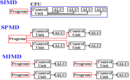
In a way, SPMD
is equivalent to MIMD in which each processor is running the same high–level
program. This does not imply running the
exact same instruction stream, as data conditionals may differ between
processors.
Multiprocessors, Multicomputers, and
Clusters
We shall now investigate
a number of strategies for parallel computing, focusing on MIMD. The two main classes of SIMD are vector
processors and array processors. We have
already discussed each, but will mention them again just to be complete.
There
are two main classes of MIMD architectures [R15]:
a) Multiprocessors,
which appear to have a shared memory and a shared address space.
b) Multicomputers,
which comprise a large number of independent processors
(each with its own memory)
that communicate via a dedicated network.
Note that each
of the SIMD and MIMD architectures call for multiple independent
processors. The main difference lies in
the instruction stream. SIMD
architectures comprise a number of processors, each executing the same set of
instructions (often in lock step). MIMD
architectures comprise a number of processors, each executing its own program.
It may be the case that a number are executing the same program; it is not
required.
Overview of Parallel Processing
Early on, it was
discovered that the design of a parallel processing system is far from trivial
if one wants reasonable performance. In
order to achieve reasonable performance, one must address a number of important
questions.
1. How
do the parallel processors share data?
2. How
do the parallel processors coordinate their computing schedules?
3. How
many processors should be used?
4. What
is the minimum speedup S(N) acceptable for N
processors?
What are the
factors that drive this decision?
In addition to
the above question, there is the important one of matching the problem to the
processing architecture. Put another
way, the questions above must be answered within the context of the problem to
be solved. For some hard real time
problems (such as anti–aircraft defense), there might be a minimum speedup that
needs to be achieved without regard to cost.
Commercial problems rarely show this dependence on a specific
performance level.
Sharing Data
There are two
main categories here, each having subcategories.
Multiprocessors are computing systems in which
all programs share a single address space.
This may be achieved by use of a single memory or a collection of memory
modules that are closely connected and addressable as a single unit. All programs running on such a system
communicate via shared variables in memory.
There are two major variants of multiprocessors: UMA and NUMA.
In UMA (Uniform Memory Access) multiprocessors, often called SMP (Symmetric Multiprocessors), each processor takes the
same amount of time to access every
memory location. This property may be
enforced by use of memory delays.
In NUMA (Non–Uniform Memory Access) multiprocessors, some memory accesses are faster than
others. This model presents interesting
challenges to the programmer in that race conditions become a real possibility,
but offers increased performance.
Multicomputers are computing systems in which a
collection of processors, each with its private memory, communicate via some
dedicated network. Programs communicate
by use of specific send message and receive message primitives. There are 2 types of multicomputers: clusters
and MPP (Massively Parallel Processors).
Coordination of Processes
Processes
operating on parallel processors must be coordinated in order to insure proper
access to data and avoid the “lost update” problem associated with stale
data. In the stale data problem, a processor uses an old copy of a data item
that has been updated. We must guarantee
that each processor uses only “fresh data”.
We shall address this issue
head–on when we address the cache coherency problem.
Classification of Parallel Processors
Here is a figure
from Tanenbaum [R15]. It shows a taxonomy of parallel computers, including SIMD, MISD, and
MIMD.
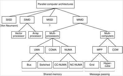
Note Tanenbaum’s sense of humor.
What he elsewhere calls a cluster, he here calls a COW for Collection of
Workstations. Here is another figure
from Tanenbaum (Ref. 4, page 549). It
shows a number of levels of parallelism including multiprocessors and
multicomputers.
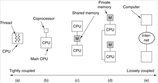
a) On–chip
parallelism, b) An attached coprocessor (we shall discuss these soon),
c) A multiprocessor with shared memory, d) A multicomputer, each processor
having
its private memory and cache, and e) A grid, which is a loosely coupled
multicomputer.
Task Granularity
This is a model
discussed by Harold Stone [R109]. It is
formulated in terms of a time–sharing model of computation. In time sharing, each process that is active
on a computer is given a fixed time allocation, called a quantum, during which it can use the CPU. At the end of its quantum, it is timed out,
and another process is given the CPU.
The Operating System will move the place a reference to the timed–out
process on a ready queue and restart
it a bit later. This model does not
account for a process requesting I/O and not being able to use its entire
quantum due to being blocked.
Let R be the
length of the run–time quantum, measured in any convenient time unit. Typical values are 10 to 100 milliseconds
(0.01 to 0.10 seconds). Let C be the
amount of time during that run–time quantum that the process spends in
communication with other processes. The
applicable ratio is (R/C), which is defined only for 0 < C £ R.
In course–grain parallelism, R/C is fairly
high so that computation is efficient.
In fine–grain parallelism, R/C is low and
little work gets done due to the excessive overhead of communication and
coordination among processors.
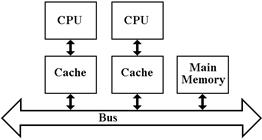
UMA Symmetric Multiprocessor
Architectures
Beginning in the
later 1980’s, it was discovered that several microprocessors can be usefully
placed on a bus. We note immediately
that, though the single–bus SMP architecture is easier to program, bus
contention places an upper limit on the number of processors that can be
attached. Even with use of cache memory
for each processor to cut bus traffic, this upper limit seems to be about 32 processors
[R15]. Here is a depiction of three
classes of bus–based UMA architectures: a) No caching,
and two variants of individual processors with caches: b) Just cache memory,
and c) Both cache memory and a private memory.
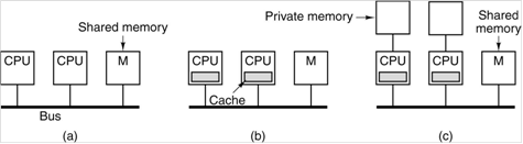
In
each architecture,
there is a global memory shared by all processors. The bus structure is not the only way to
connect a number of processors to a number of shared memories. Here are two others: the crossbar switch and
the omega switch. These are properly the
subject of a more advanced course, so we shall have little to say about them
here.
The basic idea
behind the crossbar and the omega is efficient communication among units that
form part of the computer. A typical
unit can be a CPU with an attached cache, or a memory bank. It is likely the case that there is little
memory–to–memory communication.
The figure above
shows three distinct UMA architectures.
The big issue in each of these is the proper sharing of items found in a
common global memory. For that reason,
we do not consider the third option (cache memory and private memory), as data
stored only in private memories cannot cause problems. We ignore the first option (no cache, just
direct connect to the global memory) because it is too slow and also because it
causes no problems. The only situation
that causes problems is the one with a private cache for each CPU.
Cache Coherency
A parallel
processing computer comprises a number of independent processors connected by a
communications medium, either a bus or more advanced switching system, such as
a crossbar switch. We focus this
discussion on multiprocessors, which use a common main memory as the primary
means for inter–processor communication.
Later, we shall see that many of the same issues appear for
multicomputers, which are more loosely coupled.
A big issue with
the realization of the shared–memory multiprocessors was the development of
protocols to maintain cache coherency.
Briefly put, this insures that the value in any individual processor’s
cache is the most current value and not stale data. Ideally, each processor in a multiprocessor
system will have its own “chunk of the problem”, referencing data that are not
used by other processors. Cache
coherency is not a problem in that case as the individual processors do not share
data. We shall see some situations in
which this partitioning of data can be achieved, but these are not common.
In real
multiprocessor systems, there are data that must be shared between the
individual processors. The amount of
shared data is usually so large that a single bus would be overloaded were it
not that each processor had its own cache.
When an individual processor accesses a block from the shared memory,
that block is copied into that processors cache. There is no problem as long as the processor
only reads the cache. As soon as the
processor writes to the cache, we have a cache coherency problem. Other processors accessing those data might
get stale copies. One logical way to
avoid this process is to implement each individual processor’s cache using the write–through strategy. In this strategy, the shared memory is
updated as soon as the cache is updated.
Naturally, this increases bus traffic significantly. Reduction of bus traffic is a major design
goal.
Logically
speaking, it would be better to do without cache memory. Such a solution would completely avoid the
problems of cache coherency and stale data.
Unfortunately, such a solution would place a severe burden on the
communications medium, thereby limiting the number of independent processors in
the system. This section will focus on a
common bus as a communications medium, but only because a bus is easier to
draw. The same issues apply to other
switching systems.
The Cache Write Problem
Almost all
problems with cache memory arise from the fact that the processors write data
to the caches. This is a necessary
requirement for a stored program computer.
The problem in uniprocessors is quite simple. If the cache is updated, the main memory must
be updated at some point so that the changes can be made permanent.
It was in this
context that we first met the issue of cache write
strategies. We focused on two
strategies: write–through and write–back.
In the write–through
strategy, all changes to the cache memory were immediately copied to the main
memory. In this simpler strategy, memory
writes could be slow. In the write–back strategy, changes to the
cache were not propagated back to the main memory until necessary in order to
save the data. This is more complex, but
faster.
The uniprocessor
issue continues to apply, but here we face a bigger problem.
The coherency problem arises from the fact
that the same block of the shared main memory may be resident in two or more of
the independent caches. There is no
problem with reading shared data. As
soon as one processor writes to a cache block that is found in another
processor’s cache, the possibility of a problem arises.
We first note
that this problem is not unique to parallel processing systems. Those students who have experience with
database design will note the strong resemblance to the “lost update” problem. Those
with experience in operating system design might find a hint of the theoretical
problem called “readers and writers”. It is all the same problem: handling the issues
of inconsistent and stale data. The
cache coherency problems and strategies for solution are well illustrated on a
two processor system. We shall consider
two processors P1 and P2, each with a cache.
Access to a cache by a processor involves one of two processes: read and
write. Each process can have two
results: a cache hit or a cache miss.
Recall that a cache hit occurs when the processor
accesses its private cache and finds the addressed item already in the
cache. Otherwise, the access is a cache miss. Read
hits occur when the individual processor attempts to read a data item from
its private cache and finds it there.
There is no problem with this access, no matter how many other private
caches contain the data. The problem of
processor receiving stale data on a read hit, due to updates by other
independent processors, is handled by the cache write protocols.
Cache Coherency: The Wandering Process
Problem
This strange
little problem was much discussed in the 1980’s (Ref. 3), and remains somewhat
of an issue today. Its lesser importance
now is probably due to revisions in operating systems to better assign processes
to individual processors in the system. The
problem arises in a time–sharing environment and is really quite simple. Suppose a dual–processor system: CPU_1 with
cache C_1 and CPU_2 with cache C_2.
Suppose a process P that uses data to which it has exclusive access. Consider the following scenario:
1. The
process P runs on CPU_1 and accesses its data through the cache C_1.
2. The
process P exceeds its time quantum and times out.
All dirty cache lines are
written back to the shared main memory.
3. After
some time, the process P is assigned to CPU_2.
It accesses its data
through cache C_2, updating
some of the data.
4. Again,
the process P times out. Dirty cache
lines are written back to the memory.
5. Process
P is assigned to CPU_1 and attempts to access its data. The cache C_1
retains some data from the
previous execution, though those data are stale.
In order to
avoid the problem of cache hits on stale data, the operating system must flush
every cache line associated with a process that times out or is blocked.
Cache Coherency: Snoop Tags
Each line in a
cache is identified by a cache tag (block number), which allows the
determination of the primary memory address associated with each element in the
cache. Cache blocks are identified and
referenced by their memory tags.
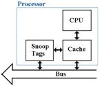
In order to
maintain coherency, each individual cache must monitor the traffic in cache
tags, which corresponds to the blocks being read from and written to the shared
primary memory. This is done by a snooping cache (or snoopy cache, after the Peanuts comic strip), which is just another
port into the cache memory from the shared bus.
The function of the snooping cache is to “snoop the bus”, watching for references to memory blocks that have
copies in the associated data cache.
Cache Coherency: A Simple Protocol
We begin our
consideration of a simple cache coherency protocol. After a few comments on this, we then move to
consideration of the MESI protocol. In
this simple protocol, each block in the cache of an individual processor can be
in one of three states:
1. Invalid:
the cache block does not contain valid data.
This might indicate that the
data in the cache are stale.
2. Shared
(Read Only): the cache block contains
valid data, loaded as a result of a
read request. The processor has not written to it; it is “clean”
in that it is not “dirty”
(been changed). This cache block may be shared with other processors;
it may
be present in a number of
individual processor caches.
3. Modified
(Read/Write): the cache block contains valid
data, loaded as a result of
either a read or write
request. The cache block is “dirty” because
its individual
processor has written to
it. It may not be shared with other individual processors,
as those other caches will
contain stale data.
A First Look at the Simple Protocol
Let’s consider
transactions on the cache when the state is best labeled as “Invalid”. The requested block is not in the individual
cache, so the only possible transitions correspond to misses, either read
misses or write misses.
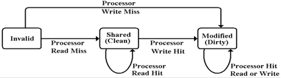
Note that this
process cannot proceed if another processor’s cache has the block labeled as
“Modified”. We shall discuss the details
of this case later. In a read miss, the individual processor
acquires the bus and requests the block.
When the block is read into the cache, it is labeled as “not dirty” and
the read proceeds.
In a write miss, the individual processor
acquires the bus, requests the block, and then writes data to its copy in the
cache. This sets the dirty bit on the
cache block. Note that the processing of
a write miss exactly follows the sequence that would be followed for a read
miss followed by a write hit, referencing the block just read.
Cache Misses: Interaction with Other
Processors
We have just
established that, on either a read miss or a write miss, the individual
processor must acquire the shared communication channel and request the block. If the requested block is not held by the
cache of any other individual processor, the transition takes place as
described above. We shall later add a
special state to account for this possibility; that is the contribution of the
MESI protocol.
If the requested
block is held by another cache and that copy is labeled as “Modified”, then a
sequence of actions must take place: 1) the modified copy is written back to
the shared primary memory, 2) the requesting processor fetches the block just
written back to the shared memory, and 3) both copies are labeled as “Shared”.
If the requested
block is held by another cache and that copy is labeled as “Shared”, then the
processing depends on the action.
Processing a read miss only requires that the requesting processor fetch
the block, mark it as “Shared”, and execute the read.
On a write miss, the requesting processor
first fetches the requested block with the protocol responding properly to the
read miss. At the point, there should be
no copy of the block marked “Modified”.
The requesting processor marks the copy in its cache as “Modified” and
sends an invalidate signal to mark
all copies in other caches as stale.
The protocol
must insure that no more than one copy of a block is marked as “Modified”.
Write Hits and Misses
As we have noted
above, the best way to view a write miss is to consider it as a sequence of
events: first, a read miss that is properly handled, and then a write hit. This is due to the fact that the only way to
handle a cache write properly is to be sure that the affected block has been
read into memory. As a result of this
two–step procedure for a write miss, we may propose a uniform approach that is
based on proper handling of write hits.
At the beginning
of the process, it is the case that no copy of the referenced block in the
cache of any other individual processor is marked as “Modified”.
If the block in
the cache of the requesting processor is marked as “Shared”, a write hit to it
will cause the requesting processor to send out a “Cache Invalidate” signal to
all other processors. Each of these
other processors snoops the bus and responds to the
Invalidate signal if it references a block held by that processor. The requesting processor then marks its cache
copy as “Modified”.
If the block in
the cache of the requesting processor is already marked as “Modified”, nothing
special happens. The write takes place
and the cache copy is updated.
The MESI Protocol
This is a
commonly used cache coherency protocol.
Its name is derived from the fours states in its FSM representation: Modified, Exclusive, Shared, and Invalid.
This description
is taken from Section 8.3 of Tanenbaum [R15].
Each
line in an individual processors cache can exist in one of the four following
states:
1. Invalid The cache line does not contain
valid data.
2. Shared Multiple caches may hold the line;
the shared memory is up to date.
3. Exclusive No other cache holds a copy of this
line;
the
shared memory is up to date.
4. Modified The line in
this cache is valid; no copies of the line exist in
other
caches; the shared memory is not up to date.
The main purpose
of the Exclusive state is to prevent the unnecessary broadcast of a Cache
Invalidate signal on a write hit. This
reduces traffic on a shared bus. Recall
that a necessary precondition for a successful write hit on a line in the cache
of a processor is that no other processor has that line with a label of
Exclusive or Modified. As a result of a successful write hit on a cache line,
that cache line is always marked as Modified.
Suppose
a requesting processor processing a write hit on its cache. By definition, any copy of the line in the
caches of other processors must be in the Shared State. What happens depends on the state of the
cache in the requesting processor.
1. Modified The protocol
does not specify an action for the processor.
2. Shared The
processor writes the data, marks the cache line as Modified,
and
broadcasts a Cache Invalidate signal to other processors.
3. Exclusive The processor writes the data and marks
the cache line as Modified.
If a line in the
cache of an individual processor is marked as “Modified” and another processor
attempts to access the data copied into that cache line, the individual
processor must signal “Dirty” and write the data back to the shared primary
memory.
Consider
the following scenario, in which processor P1 has a write miss on a cache line.
1. P1
fetches the block of memory into its cache line, writes to it, and marks it
Dirty.
2. Another
processor attempts to fetch the same block from the shared main memory.
3. P1’s
snoop cache detects the memory request.
P1 broadcasts a message “Dirty” on
the shared bus, causing the
other processor to abandon its memory fetch.
4. P1
writes the block back to the share memory and the other processor can access
it.
Events in the MESI Protocol
There are six
events that are basic to the MESI protocol, three due to the local processor
and three due to bus signals from remote processors [R110].
Local
Read The individual processor
reads from its cache memory.
Local
Write The individual processor
writes data to its cache memory.
Local
Eviction The individual processor must
write back a dirty line from its
cache in order
to free up a cache line for a newly requested block.
Bus
Read Another processor issues a
read request to the shared primary
memory for a
block that is held in this processors individual cache.
This
processor’s snoop cache detects the request.
Bus
Write Another processor issues a
write request to the shared primary
memory for a
block that is held in this processors individual cache.
Bus
Upgrade Another processor signals
that a write to a cache line that is shared
with this
processor. The other processor will
upgrade the status of
the cache line
from “Shared” to “Modified”.
The MESI FSM: Action and Next State (NS)
Here is a
tabular representation of the Finite State Machine for the MESI protocol.
Depending on its Present State (PS), an individual processor responds to
events.
|
PS
|
Local Read
|
Local
Write
|
Local
Eviction
|
BR
Bus Read
|
BW
Bus Write
|
BU – Bus
Upgrade
|
|
I Invalid
|
Issue BR
Do other caches have this line.
Yes: NS = S
No: NS = E
|
Issue BW
NS = M
|
NS = I
|
Do
nothing
|
Do
nothing
|
Do
nothing
|
|
S
Shared
|
Do nothing
|
Issue BU
NS = M
|
NS = I
|
Respond
Shared
|
NS = I
|
NS = I
|
|
E Exclusive
|
Do nothing
|
NS = M
|
NS = I
|
Respond Shared
NS = S
|
NS = I
|
Error
Should not occur.
|
|
M Modified
|
Do nothing
|
Do
nothing
|
Write data back.
NS = I.
|
Respond Dirty.
Write data back
NS = S
|
Respond Dirty.
Write data back
NS = I
|
Error
Should not occur.
|
MESI Illustrated
Here is an
example from the text by Andrew Tanenbaum [R15]. This describes three individual processors,
each with a private cache, attached to a shared primary memory. When the
multiprocessor is turned on, all cache lines are marked invalid. We begin
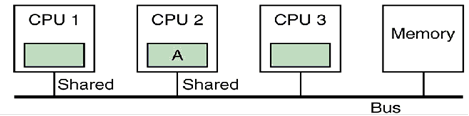
with CPU reading block A from the shared memory.
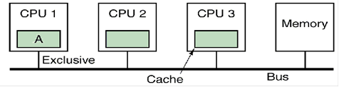
CPU 1 is the
first (and only) processor to request block A from the
shared memory. It issues a BR (Bus Read)
for the block and gets its copy. The
cache line containing block A is marked Exclusive. Subsequent reads to this block access the
cached entry and not the shared memory.Neither CPU 2 nor CPU 3 respond to the BR.
We now assume
that CPU 2 requests the same block. The
snoop cache on CPU 1 notes the request and CPU 1 broadcasts “Shared”,
announcing that it has a copy of the block.
Both copies of
the block are marked as shared. This
indicates that the block is in two or more caches for reading and that the copy
in the shared primary memory is up to date.
CPU 3 does not respond to the BR. At
this point, either CPU 1 or CPU 2 can issue a local write, as that step is
valid for either the Shared or Exclusive state.
Both are in the Shared state. Suppose
that CPU 2 writes to the cache line it is holding in its cache. It issues a BU (Bus Upgrade) broadcast, marks
the cache line as Modified, and writes the data to the line.
CPU 1 responds
to the BU by marking the copy in its cache line as Invalid.
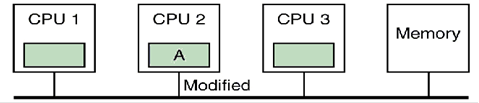
CPU 3 does not
respond to the BU. Informally, CPU 2 can
be said to “own the cache line”.
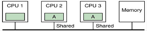
Now suppose that
CPU 3 attempts to read block A from primary memory. For CPU 1, the cache line holding that block
has been marked as Invalid. CPU 1 does
not respond to the BR (Bus Read) request.
CPU 2 has the cache line marked as Modified. It asserts the signal “Dirty” on the bus,
writes the data in the cache line back to the shared memory, and marks the line
“Shared”. Informally, CPU 2 asks CPU 3
to wait while it writes back the contents of its modified cache line to the
shared primary memory. CPU 3 waits and
then gets a correct copy. The cache line
in each of CPU 2 and CPU 3 is marked as Shared.
Summary
We have
considered cache memories in parallel computers, both multiprocessors and
multicomputers. Each of these
architectures comprises a number of individual processors with private caches
and possibly private memories. We have
noted that the assignment of a private cache to each of the individual
processors in such architecture is necessary if we are to get acceptable
performance. We have noted that the
major issue to consider in these designs is that of cache coherency. Logically
speaking, each of the individual processors must function as if it were
accessing the one and only copy of the memory block, which resides in the
shared primary memory.
We have proposed
a modern solution, called MESI, which is a protocol in the class called “Cache
Invalidate”. This shows reasonable
efficiency in the maintenance of coherency.
The only other
class of protocols falls under the name “Central Database”. In this, the shared primary memory maintains
a list of “which processor has which block”.
This centralized management of coherency has been shown to place an
unacceptably high processing load on the shared primary memory. For this reason, it is no longer used.
Loosely Coupled Multiprocessors
Our previous
discussions of multiprocessors focused on systems built with a modest number of
processors (no more than about 50), which communicate via a shared bus. The class of computers we shall consider now
is called “MPP”, for Massively Parallel Processor”. As we shall see, the development of MPP
systems was resisted for a long time, due to the belief that such designs could
not be cost effective. We shall see that
MPP systems finally evolved due to a number of factors, at least one of which
only became operative in the late 1990’s.
1. The availability of small and
inexpensive microprocessor units (Intel 80386, etc.)
that could be efficiently
packaged into a small unit.
2. The discovery that many very important
problems were quite amenable to
parallel implementation.
3. The discovery that many of these
important problems had structures of such
regularity that sequential
code could be automatically translated for parallel
execution with little loss in
efficiency.
Early History: The C.mmp
While this chapter
will focus on multicomputers, it is instructive to begin with a review of a
paper on the C.mmp, which is a shared–memory multiprocessor developed at
Carnegie Mellon University in the early 1970’s.
The C.mmp is described in a paper by Wulf and Harbinson [R111], which has been noted as “one of the most
thorough and balanced research–project retrospectives … ever seen”. Remarkably, this paper gives a thorough
description of the project’s failures.
The C.mmp is described [R111] as “a multiprocessor composed of
16 PDP–11’s, 16 independent memory banks, a crosspoint
[crossbar] switch which permits any processor to access any memory, and a
typical complement of I/O equipment”. It
includes an independent bus, called the “IP bus”, used to communicate control
signals.
As of 1978, the
system included the following 16 processors.
5 PDP–11/20’s, each rated at 0.20
MIPS (that is 200,000 instructions per second)
11 PDP–11/40’s, each rated at 0.40
MIPS
3 megabytes of shared memory (650 nsec core and 300 nsec
semiconductor)
The system was
observed to compute at 6 MIPS.
The Design Goals of the C.mmp
The goal of the
project seems to have been the construction of a simple system using as many
commercially available components as possible.
The C.mmp was intended to be a research project not only in distributed
processors, but also in distributed software.
The native operating system designed for the C.mmp was called “Hydra”. It was intended as an OS kernel, intended to
provide only minimal services and encourage experimentation in system software. As of 1978, the software developed on top of
the Hydra kernel included file systems, directory systems, schedulers and a
number of language processors.
Another part of
the project involved the development of performance evaluation tools, including
the Hardware Monitor for recording the signals on the PDP–11 data bus and
software tools for analyzing the performance traces. One of the more important software tools was
the Kernel Tracer, which was built into the Hydra kernel. It allowed selected operating system events,
such as context swaps and blocking on semaphores, to be recorded while a set of
applications was running. The Hydra
kernel was originally designed based on some common assumptions. When experimentation showed these to be
false, the Hydra kernel was redesigned.
The C.mmp: Lessons Learned
The researchers
were able to implement the C.mmp as “a cost–effective, symmetric multiprocessor”
and distribute the Hydra kernel over all of the processors. The use of two variants of the PDP–11 was
considered as a mistake, as it complicated the process of making the necessary
processor and operating system modifications.
The authors had used newer variants of the PDP–11 in order to gain
speed, but concluded that “It would have been better to have had a single
processor model, regardless of speed”. The
critical component was expected to be the crossbar switch. Experience showed the switch to be “very
reliable, and fast enough”. Early
expectations that the “raw speed” of the switch would be important were not
supported by experience.
The authors
concluded that “most applications are sped up by decomposing their algorithms
to use the multiprocessor structure, not by executing on processors with short memory
access times”. The simplicity of the
Hydra kernel, with much system software built on top of it, yielded benefits,
such as few software errors caused by inadequate synchronization.
The C.mmp:
More Lessons Learned
Here
I quote from Wulf & Harbison
[R111], arranging their comments in an order not found in their original. The PDP–11 was a memory–mapped architecture
with a single bus, called the UNIBUS, that connected
the CPU to both memory and I/O devices.
1. “Hardware
(un)reliability was our largest day–to–day disappointment … The
aggregate
mean–time–between–failure (MTBF) of C.mmp/Hydra fluctuated
between two to six hours.”
2. “About
two–thirds of the failures were directly attributable to hardware
problems.
There is insufficient fault detection
built into the hardware.”
3. “We
found the PDP–11 UNIBUS to be especially noisy and error–prone.”
4. “The
crosspoint [crossbar] switch is too trusting of other
components; it can be
hung by malfunctioning
memories or processors.”
My favorite
lesson learned is summarized in the following two paragraphs in the report.
“We made a serious error in not
writing good diagnostics for the hardware.
The software developers should have written such programs for the
hardware.”
“In our experience, diagnostics
written by the hardware group often did not test components under the type of
load generated by Hydra, resulting in much finger–pointing between groups.”
The Challenge for Multiprocessors
As
multicore processors evolve into manycore processors (with a few hundreds of
cores), the challenge remains the same as it always has been. The goal is to
get an increase in computing power (or performance or whatever) that is
proportional to the cost of providing a large number of processors. The design problems associated with multicore
processors remain the same as they have always been: how to coordinate the work
of a large number of computing units so that each is doing useful work. These problems generally do not arise when
the computer is processing a number of independent jobs that do not need to
communicate. The main part of these
design problems is management of access to shared memory. This part has two aspects:
1. The
cache coherency problem, discussed earlier.
2. The
problem of process synchronization, requiring the use of lock
variables, and reliable
processes to lock and unlock these variables.
Task Management in Multicomputers
The basic idea
behind both multicomputers and multiprocessors is to run multiple tasks or
multiple task threads at the same time.
This goal leads to a number of requirements, especially since it is
commonly assumed that any user program will be able to spawn a number of
independently executing tasks or processes or threads.
According
to Baron and Higbie [R112], any multicomputer or
multiprocessor system must provide facilities for these five task–management
capabilities.
1. Initiation A process must be able to spawn another process;
that
is, generate another process and activate it.
2. Synchronization A process must be able to suspend itself or another process
until
some sort of external synchronizing event occurs.
3. Exclusion A process must be able to monopolize a shared
resource,
such
as data or code, to prevent “lost updates”.
4. Communication A process must be able to exchange messages with any
other
active process that is executing on the system.
5. Termination A process must be able to terminate itself and release
all
resources being used, without any memory leaks.
These facilities
are more efficiently provided if there is sufficient hardware support.
Multiprocessors
One of the more
common mechanisms for coordinating multiple processes in a single address space
multiprocessor is called a lock. This feature is commonly used in databases
accessed by multiple users, even those implemented on single processors.
Multicomputers
These must use
explicit synchronization messages in order to coordinate the processes. One method is called “barrier synchronization”, in which there are logical spots, called
“barriers” in each of the programs. When
a process reaches a barrier, it stops processing and waits until it has
received a message allowing it to proceed.
The common idea is that each processor must wait at the barrier until
every other processor has reached it. At
that point every processor signals that it has reached the barrier and received
the signal from every other processor.
Then they all continue.
Other
processors, such as the MIPS, implement a different mechanism.
A Naive Lock Mechanism and Its Problems
Consider
a shared memory variable, called LOCK,
used to control access to a specific shared resource. This simple variable has two values. When the variable has value 0, the lock is free
and a process may set the lock value to 1 and obtain the resource. When the variable has value 1, the lock is
unavailable and any process must wait to have access to the resource. Here is the simplistic code (written in Boz–7
assembly language) that is executed by any process to access the variable.
GETIT LDR %R1,LOCK LOAD THE LOCK VALUE INTO R1.
CMP %R1,%R0 IS THE VALUE 0? REMEMBER THAT
REGISTER R0 IS
IDENTICALLY 0.
BGT GETIT NO, IT IS 1. TRY AGAIN.
LDI %R1,1 SET THE REGISTER TO VALUE 1
STR %R1,LOCK STORE VALUE OF 1, LOCKING IT
The Obvious Problem
We
suppose a context switch after process 1 gets the lock and before it is able to
write
the revised lock value back to main memory.
It is a lost update.
Event Process
1 Process
2
LOCK
= 0
LDR %R1,LOCK
%R1 has value 0
CMP %R1,%R0
Compares OK. Continue
Context
switch LDR
%R1,LOCK
%R1 has
value 0
Set
LOCK = 1
Continue
LOCK = 1
Context switch LDI
%R1,1
STR %R1,LOCK
Continue
LOCK = 1
Each process has
access to the resource and continues processing.
Hardware Support for Multitasking
Any processor or
group of processors that supports multitasking will do so more efficiently if
the hardware provides an appropriate primitive operation. A test–and–set
operation with a binary semaphore
(also called a “lock variable”) can
be used for both mutual exclusion and process synchronization. This is best implemented as an atomic operation, which in this context
is one that cannot be interrupted until it completes execution. It either executes completely or fails.
Atomic Synchronization Primitives
What is needed
is an atomic operation, defined in the original sense of the word to be an
operation that must complete once it begins.
Specifically it cannot be interrupted or suspended by a context switch. There may be some problems associated with
virtual memory, particularly arising from page faults. These are easily fixed. We consider an atomic
instruction that is to be called CAS, standing for either Compare and Set, or
Compare and Swap
Either of these
takes three arguments: a lock variable, an expected value (allowing the
resource to be accessed) and an updated value (blocking access by other processes
to this resource). Here is a sample of
proper use.
LDR %R1,LOCK ATTEMPT
ACCESS, POSSIBLY
CAUSING A PAGE
FAULT
CAS LOCK,0,1 SET TO 1 TO
LOCK IT.
Two Variants of CAS
Each variant is
atomic; it is guaranteed to execute with no interrupts or
context switches. It is a single CPU
instruction, directly executed by
the hardware.
Compare_and_set (X, expected_value, updated_value)
If (X == expected_value)
X ¬ updated_value
Return
True
Else Return False
Compare_and_swap (X, expected_value, updated_value)
If (X == expected_value)
Swap X « updated_value
Return
True
Else Return False
Such
instructions date back at least to the IBM System/370 in 1970.
What About
MESI?
Consider two
processes executing on different processors, each with its own cache memory
(probably both L1 and L2). Let these
processes be called P1 and P2. Suppose
that each P1 and P2 have the variable LOCK
in cache memory and that each wants to set it.
Suppose P1 sets
the lock first. This write to the cache
block causes a cache invalidate to
be broadcast to all other processes. The
shared memory value of LOCK is
updated and then copied to the cache associated with process P2. However, there is no signal to P2 that the value
in its local registers has become invalid.
P2 will just write a new value to its cache. In other words, the MESI protocol will maintain
the integrity of values in shared memory.
However, it cannot be used as a lock mechanism. Any synchronization primitives that we design
will assume that the MESI protocol is functioning properly and add important
functionality to it.
CAS: Implementation Problems
The
single atomic CAS presents some problems in processor design, as it requires
both a memory read and memory write in a single uninterruptable instruction. The option chosen by the designers of the
MIPS is to create a pair of instructions in which the second instruction
returns a value showing whether or not the two executed as if they were atomic. In the MIPS design, this pair of instructions
is as follows:
LL Load
Linked LL Register, Memory Address
SC Store
Conditional SC Register, Memory Address
This
code
either fails or swaps the value in register $S4 with the value in
the memory location with address in register $S1.
TRY: ADD $T0,$0,$S4 MOVE VALUE
IN $S4 TO REGISTER $T0
LL $T1,0($S1) LOAD $T1 FROM MEMORY ADDRESS
SC $T0,0($S1) STORE CONDITIONAL
BEQ $T0,$0,TRY BRANCH
STORE FAILS, GO BACK
ADD $S4,$0,$T1 PUT VALUE
INTO $S4
More on the MESI Issue
Basically the
MESI protocol presents an efficient mechanism to handle the effects of
processor writes to shared memory. MESI
assumes a shared memory in which each addressable item has a unique memory
address and hence a unique memory block number.
But
note that the problem associated with MESI would largely go away if we could
make one additional stipulation: once a block in shared memory is written by a
processor, only that processor will access that block for some time. We shall see that a number of problems have
this desirable property. We may assign
multiple processors to the problem and enforce the following.
a) Each
memory block can be read by any number of processors,
provided that it is only read.
b) Once
a memory block is written to by one processor, it is the “sole property”
of that processor. No other processor may read or write that
memory block.
Remember that a
processor accesses a memory block through its copy in cache.
The High–End Graphics Coprocessor and
CUDA
We now proceed
to consider a type of Massively Parallel Processor and a class of problems well
suited to be executed on processors of this class. The main reason for this match is the
modification to MESI just suggested. In
this class of problems, the data being processed can be split into small sets,
with each set being assigned to one, and only one, processor. The original problems of this class were
taken from the world of computer graphics and focused on rendering a digital
scene on a computer screen. For this
reason, the original work on the class of machines was done under the name GPU
(Graphical Processing Unit). In the
early development, these were nothing more than high performance graphic cards.
Since about
2003, the design approach taken by NVIDIA Corporation for these high end
graphical processing units has been called “many–core” to distinguish it from the more traditional multicore
designs found in many commercial personal computers. While a multicore CPU might have 8 to 16
cores, a many–core GPU will have hundreds of cores. In 2008, the NVIDIA GTX 280 GPU had 280 cores
[R68]. In July 2011, the NVIDIA Tesla
C2070 had 448 cores and 6 GB memory [R113].
The historic
pressures on the designers of GPUs are well described by Kirk & Hwu [R68].
“The design
philosophy of the GPUs is shaped by the fast growing video game industry, which
exerts tremendous economic pressure for the ability to perform a massive number
of floating–point calculations per video frame in advanced games. … The prevailing solution to date is to
optimize for the execution throughput of massive numbers of threads. … As a result, much more chip area is
dedicated to the floating–point calculations.”
“It should be
clear now that GPUs are designed as numeric computing engines, and they will
not perform well on some tasks on which CPUs are designed to perform well;
therefore, one should expect that most applications will use both CPUs and
GPUs, executing the sequential parts on the CPU and the numerically intensive
parts on the GPUs. This is why the CUDA™
(Compute Unified Device Architecture) programming model,
introduced by NVIDIA in 2007, is designed to support joint CPU/GPU execution of
an application.”
Game Engines as Supercomputers
It may surprise
students to learn that many of these high–end graphics processors are actually
export controlled as munitions. In this
case, the control is due to the possibility of using these processors as
high–performance computers.
In the figure
below, we present a high–end graphics coprocessor that can be viewed as a
vector processor. It is capable of a
sustained rate of 4,300 Megaflops.
The NVIDIA Tesla C870
Data here are
from the NVIDIA web site [R113]. I quote
from their advertising copy from the year 2008.
This is impressive enough; I did not bother with the figures for this
year.
 The C870
processor is a “massively multi–threaded processor architecture that is ideal
for high performance computing (HPC) applications”.
The C870
processor is a “massively multi–threaded processor architecture that is ideal
for high performance computing (HPC) applications”.
This has 128
processor cores, each operating at 1.35 GHz.
It supports the IEEE–754 single–precision standard, and operates at a
sustained rate of 430 gigaflops (512 GFlops peak).
The typical
power usage is 120 watts. Note the
dedicated fan for cooling.
The processor
has 1.5 gigabytes of DDR SDRAM, operating at 800 MHz. The data bus to memory is 384 bits (48 bytes)
wide, so that the maximum sustained data rate is 76.8 Gigabytes per second.
Compare this to
the CRAY–1 supercomputer of 1976, with a sustained computing rate of 136
Megaflops and a peak rate of 250 Megaflops.
This is about 3.2% of the performance of the current graphics
coprocessor at about 500 times the cost.
The Cray Y–MP was a supercomputer sold by Cray Research beginning in
1988. Its peak performance was 2.66
Gigaflops (8 processors at 333 Megaflops each).
Its memory comprised 128, 256, or 512 MB of static RAM. The earliest supercomputer that could
outperform the current graphics processor seems to have been the Cray
T3E–1200E™, a MPP (Massively Parallel Processor) introduced in 1995 (Ref.
9). In 1998, a joint scientific team
from Oak Ridge National Lab, the University of Bristol (UK) and others ran a
simulation related to controlled fusion at a sustained rate of 1.02 Teraflops
(1020 Gigaflops).
Sample Problem: 2–D Matrix
Multiplication
We now turn to a
simple mathematics problem that illustrates the structure of a problem that is
well suited to execution on the GRU part of the CUDA. We shall begin with simple sequential code
and modify it in stages until it is structured for parallel execution.
Here we consider
the multiplication of two square matrices, each of size N–by–N, having row and column indices in the range [0, N – 1]. The following is code such as one might see
in a typical serial implementation to multiply square matrix A by square matrix
B, producing square matrix C.
For I = 0
to (N – 1) Do
For J = 0
to (N – 1) Do
Sum = 0 ;
For K =
0 to (N – 1) Do
SUM
= SUM + A[I][K]·B[K][J] ;
End For
C[I][J] = SUM ;
End For
End For
Note the use of SUM to avoid multiple references to C[I][J] within the inner loop.
Memory Organization of 2–D Arrays
In order to
write efficient array code of any sort one has to understand the organization
of multiply dimensioned arrays in computer memory. The most efficient way to handle two
dimensional arrays will be to treat them as one dimensional arrays. We are moving towards a parallel
implementation in which the computation of any number of matrix functions of
two square N–by–N matrices can be done very efficiently in parallel by an array
of N2 processors; each computing the results for one element in the
result array.
Doing this
efficiently means that we must reduce all arrays to one dimension, in the way
that the run–time support systems for high–level languages do. Two–dimensional arrays make for good examples
of this in that they represent the simplest data structures in which this
effect is seen. Multiply dimensioned
arrays are stored in one of two fashions: row major order and column major order. Consider a 2–by–3 array X.
In row major
order, the rows are stored contiguously.
X[0][0], X[0][1], X[0][2], X[1][0], X[1][1], X[1][0]
Most high–level
languages use row major ordering.
In column major
order, the columns are stored contiguously
X[0][0], X[1][0], X[0][1], X[1][1], X[0][2], X[1][2]
Old FORTRAN is
column major.
We shall assume
that the language for implementing this problem supports row major
ordering. In that case, we have two ways
to reference elements in the array.
Two indices X[0][0] X[0][1] X[0][2] X[1][0] X[1][1] X[1][0]
One index X[0] X[1] X[2] X[3] X[4] X[5]
The index in the “one index”
version is the true offset of the element in the array.
Sample Problem Code Rewritten
The following is
code shows the one–dimensional access to the 2–dimensional
arrays A, B, C. Each has row and column
indices in the range [0, N – 1].
For I = 0
to (N – 1) Do
For J = 0
to (N – 1) Do
Sum = 0 ;
For K =
0 to (N – 1) Do
SUM
= SUM + A[I·N + K]·B[K·N + J] ;
End For
C[I·N + J] = SUM ;
End For
End For
Note that the [I][J] element of an
N–by–N array is at offset [I·N + J].
Some Issues of Efficiency
The first issue
is rather obvious and has been assumed. We
might have written the code as:
For K =
0 to (N – 1) Do
C[I·N + J] = C[I·N + J] + A[I·N + K]·B[K·N + J] ;
End For
But note that
this apparently simpler construct leads to 2·N
references to array element C[I·N + J] for each value of I and J. Array references are expensive, because the
compiler must generate code that will allow access to any element in the array.
Our code has one
reference to C[I·N + J] for each value of I and J.
Sum = 0 ;
For K =
0 to (N – 1) Do
SUM
= SUM + A[I·N + K]·B[K·N + J] ;
End For
C[I·N + J] = SUM ;
Array Access: Another Efficiency Issue
In this
discussion, we have evolved the key code statement as follows. We began with
SUM = SUM + A[J][L]·B[L][K] and changed to
SUM = SUM + A[I·N + K]·B[K·N + J]
The purpose of
this evolution was to make explicit the mechanism by which the address of an
element in a two–dimensional array is determined. This one–dimensional access code exposes a
major inefficiency that is due to the necessity of multiplication to determine
the addresses of each of the two array elements in this statement. Compared to addition, multiplication is a
very time–consuming operation.
As written the
key statement SUM = SUM + A[I·N
+ K]·B[K·N + J] contains three multiplications, only
one of which is essential to the code. We
now exchange the multiplication statements in the address computations for
addition statements, which execute much more quickly.
Addition to Generate Addresses in a Loop
Change the inner
loop to define and use the indices L
and M as follows.
For K =
0 to (N – 1) Do
L =
I·N + K ;
M =
K·N + J ;
SUM
= SUM + A[L]·B[M] ;
End For
For
K = 0 L = I·N M = J
For
K = 1 L = I·N + 1 M = J + N
For
K = 2 L = I·N + 2 M = J + 2·N
For K = 3 L = I·N + 3 M = J + 3·N
The Next Evolution of the Code
This example
eliminates all but one of the unnecessary multiplications.
For I = 0
to (N – 1) Do
For J = 0
to (N – 1) Do
Sum = 0 ;
L = I·N ;
M =
J ;
For K =
0 to (N – 1) Do
SUM
= SUM + A[L]·B[M] ;
L =
L + 1 ;
M =
M + N ;
End For
C[I·N + J] = SUM ;
End For
End For
Suppose a Square Array of Processors
Suppose an array
of N2 processors, one for each element in the product array C. Each of these processors will be assigned a
unique row and column pair. Assume that
process (I, J) is running on processor (I, J) and that there is a global
mechanism for communicating these indices to each process.
Sum = 0 ;
L = I·N ;
M =
J ;
INJ = L
+ M ; // Note
we have I·N + J computed
here.
For K =
0 to (N – 1) Do
SUM
= SUM + A[L]·B[M] ;
L =
L + 1 ;
M =
M + N ;
End For
C[INJ]
= SUM ;
For large values
of N, there is a significant speedup to be realized.
Another Look at the NVIDIA GeForce 8800
GTX
Here, your
author presents a few random thoughts about this device. As noted in the textbook, a “fully loaded”
device has 16 multiprocessors, each of which contains 8 streaming processors
operating at 1.35 GHz. Each streaming
processor has a local memory with capacity of 16 KB, along with 8,192 (213)
32–bit registers.
The work load
for computing is broken into threads, with a thread block being defined as a number of intercommunicating threads
that must execute on the same streaming processor. A block can have up to 512 (29)
threads.
Conjecture: This
division allows for sixteen 32–bit registers per thread.
Fact: The maximum
performance of this device is 345.6 GFLOPS
(billion
floating point operations per second)
On
4/17/2010, the list price was $1320 per unit, which was
discounted
to $200 per unit on Amazon.com.
Fact: In
1995, the fastest vector computer was a Cray T932. Its maximum
performance
was just under 60 GFLOPS. It cost $39
million.
Some Final Words on CUDA
As has been
noted above in this text, the graphical processing units are designed to be
part of a computational pair, along with a traditional CPU. Examination of the picture of the NVIDIA Tesla
C870 shows it to be a coprocessor, to be attached to the main computer
bus. It turns out that the device uses a
PCI Express connection.
The best way to
use a CUDA is to buy an assembled PC with the GPU attached. Fortunately these are quite reasonable. In July 2011, one could buy a Dell Precision
T7500 with a Quad Core Xeon Processor (2.13 GHz), 4 GB of DDR3 RAM, a 250 GB
SATA disk, and an attached NVIDIA Tesla C2050, all for about $5,000.
Clusters, Grids, and the Like
There are many
applications amenable to an even looser grouping of multicomputers. These often use collections of commercially
available computers, rather than just connecting a number of processors
together in a special network. In the
past there have been problems of administering large clusters of computers; the
cost of administration scaling as a linear function of the number of
processors. Recent developments in
automated tools for remote management are likely to help here.
It appears that blade servers are one of the more
recent adaptations of the cluster concept.
The major advance represented by blade servers is the ease of mounting
and interconnecting the individual computers, called “blades”, in the cluster. In
this aspect, the blade server hearkens back to the 1970’s and the innovation in
instrumentation called “CAMAC”, which was a rack with a standard bus structure
for interconnecting instruments. This
replaced the jungle of interconnecting wires, so complex that it often took a
technician dedicated to keeping the communications intact.
Clusters can be
placed in physical proximity, as in the case of blade servers, or at some
distance and communicate via established networks, such as the Internet. When a network is used for communication, it
is often designed using TCP/IP on top of Ethernet simply due to the wealth of
experience with this combination.
A Few Examples
of Clusters, Grids, and the Like
In
order to show the variety of large computing systems, your author has selected
a random collection. Each will be
described in a bit of detail.
The E25K NUMA
Multiprocessor by Sun Microsystems
Our first
example is a shared–memory NUMA multiprocessor built from seventy–two
processors. Each processor is an UltraSPARC IV, which itself is a pair of UltraSPARC III Cu processors. The “Cu” in the name refers to the use of
copper, rather than aluminum, in the signal traces on the chip. A trace
can be considered as a “wire” deposited on the surface of a chip; it carries a
signal from one component to another.
Though more difficult to fabricate than aluminum traces, copper traces
yield a measurable improvement in signal transmission speed, and are becoming
favored.
Recall that NUMA
stands for “Non–Uniform Memory Access” and describes those multiprocessors in
which the time to access memory may depend on the module in which the addressed
element is located; access to local memory is much faster than access to memory
on a remote node. The basic board in the
multiprocessor comprises the following:
1. A CPU and memory board with four UltraSPARC IV processors, each with an 8–GB
memory. As each processor is dual core, the board has
8 processors and 32 GB memory.
2. A snooping bus between the four processors,
providing for cache coherency.
3. An I/O board with four PCI slots.
4. An expander board to connect all of these
components and provide communication
to the other boards in the
multiprocessor.
A full E25K
configuration has 18 boards; thus 144 CPU’s and 576 GB of memory.
The E25K Physical Configuration
Here is a figure
from Tanenbaum [R15] depicting the E25K
configuration.
The E25K has a centerplane with three 18–by–18 crossbar switches to
connect the boards. There is a crossbar
for the address lines, one for the responses, and one for data transfer.
The number 18
was chosen because a system with 18 boards was the largest that would fit through
a standard doorway without being disassembled.
Design constraints come from everywhere.
Cache Coherence in the E25K
How does one
connect 144 processors (72 dual–core processors) to a distributed memory and
still maintain cache coherence? There
are two obvious solutions: one is too slow and the other is too expensive. Sun Microsystems opted for a multilevel
approach, with cache snooping on each board and a directory structure at a
higher level. The next figure shows the
design.
The memory
address space is broken into blocks of 64 bytes each. Each block is assigned a “home board”, but
may be requested by a processor on another board. Efficient algorithm design will call for most
memory references to be served from the processors home board.
The IBM BlueGene
The description
of this MPP system is based mostly on Tanenbaum [R15]. The system was designed in 1999 as “a
massively parallel supercomputer for solving computationally–intensive problems
in, among other fields, the life sciences”.
It has long been known that the biological activity of any number of
important proteins depends on the three dimensional structure of the
protein. An ability to model this three
dimensional configuration would allow the development of a number of powerful
new drugs.
The BlueGene/L was the first model built; it was shipped to
Lawrence Livermore Lab in June 2003. A
quarter–scale model, with 16,384 processors, became operational in November
2004 and achieved a computational speed of 71 teraflops. The full model, with 65,536 processors, was
scheduled for delivery in the summer of 2005.
In October 2005, the full system achieved a peak speed on 280.6
teraflops on a standard benchmark called “Linpack”. On real problems, it achieved a sustained
speed of over 100 teraflops.
The Custom Processor Chip
IBM intended the
BlueGene line for general commercial and research
applications. Because of this, the
company elected to produce the processor chips from available commercial cores. Each processor chip has two PowerPC 440 cores
operating at 700 MHz.
The configuration of the chip, with its multiple caches is shown in the
figure below. Note that only one of the
two cores is dedicated to computation, the other is dedicated to handling
communications.
The connection
topology used in the BlueGene is a three–dimensional
torus. Each processor chip is connected
to six other processor chips. The
connections are called “North”, “East”, “South”, “West”, “Up”, and “Down”. Think of a three–dimensional cube with 6
faces.
In a recent
upgrade (June 2007), IBM upgraded this chip to hold
four PowerPC 450 cores operating at 850 MHz. In November 2007, the new computer, called
the BlueGene/P achieved a sustained performance of
167 teraflops. This design obviously has
some “growing room”.
The BlueGene/L
Hierarchy
The 65,536 BlueGene/L is designed in a hierarchical fashion. There are two chips per card,
16 cards per board, 32 boards per cabinet, and 64 cabinets in the system.
We shall see
that the MPP systems manufactured by Cray, Inc. follow the same design
philosophy. It seems that this
organization will become common for large MPP systems.
The AMD Opteron
Before
continuing with our discussion of MPP systems, let us stop and examine the chip
that has recently become the favorite for use as the processor, of which there
are thousands. This chip is the AMD
Opteron, which is a 64–bit processor that can operate in three modes.
In legacy mode, the Opteron runs standard
Pentium binary programs unmodified.
In compatibility mode, the operating
system runs in full 64–bit mode, but applications
must run in 32–bit mode.
In 64–bit mode, all programs can issue
64–bit addresses; both 32–bit and 64–bit
programs can run simultaneously in this mode.
The Opteron has
an integrated memory controller, which runs at the speed of the processor
clock. This improves memory
performance. It can manage 32 GB of
memory. The Opteron comes in
single–core, dual–core, or quad–core processors. The standard clock rates for these processors
range from 1.7 to 2.3 GHz.
The Red Storm by
Cray, Inc.
The Red Storm is
a MPP system in operation at Sandia National Laboratory. This lab, operated by Lockheed Martin, doe
classified work for the U.S. Department of Energy. Much of this work supports the design of
nuclear weapons. The simulation of
nuclear weapon detonations, which is very computationally intensive, has
replaced actual testing as a way to verify designs.
In 2002, Sandia
selected Cray, Inc. to build a replacement for its current MPP, called ASCI
Red. This system had 1.2 terabytes of
RAM and operated at a peak rate of 3 teraflops.
The Red Storm was delivered in August 2004 and upgraded in 2006 [Ref.
9]. The Red Storm now uses dual–core AMD
Opterons, operating at 2.4 GHz. Each Opteron has 4 GB of RAM and a dedicated
custom network processor called the Seastar,
manufactured by IBM. Almost all data
traffic between processors moves through the Seastar network, so great care was
taken in its design. This is the only
chip that is custom–made for the project.
The next step in
the architecture hierarchy is the board,
which holds four complete Opteron systems (four CPU’s, 16 GB RAM, four Seastar
units), a 100 megabit per second Ethernet chip, and a RAS (Reliability,
Availability, and Service) processor to facilitate fault location. The next step in the hierarchy is the card cage, which comprises eight boards
inserted into a backplane. Three card
cages and their supporting power units are placed into a cabinet. The full Red Storm system comprises 108
cabinets, for a total of 10,836 Opterons and 10 terabytes of SDRAM. Its theoretical peak performance is 124
teraflops, with a sustained rate of 101 teraflops (1012
floating–point operations per second).
Security Implications of the
Architecture
In the world on
national laboratories there are special requirements on the architecture of
computers that might be used to process classified data. The Red Storm at Sandia routinely processes
data from which the detailed design of current U.S. nuclear warheads may be
inferred. Naturally, such data are considered
to be quite sensitive. The solution to
the security problem was to partition Red Storm into classified and
unclassified sections. This partitioning
was done by mechanical switches, which would completely isolate one section
from another. There are three sections:
classified, unclassified, and a switchable section.
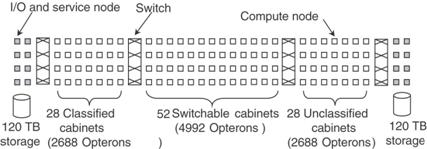
The Cray XT5h
The Cray XT3 is
a commercial design based on the Red Storm installed at Sandia National Labs. The Cray XT3 led to the development of the
Cray XT4 and Cray XT5, the latest in the line.
The XT5 follows the Red Storm approach in using a large number of AMD
Opteron processors. The processor
interconnect uses the same three–dimensional torus as found in the IBM BlueGene and presumably in the Cray Red Storm. The network processor has been upgraded to a
system called ‘Seastar 2+”; each switch having six 9.6 GB/second
router–to–router ports.
The Cray XT5h is
a modified XT5, adding vector coprocessors and FPGA (Field Programmable Gate
Array) accelerators. FPGA processors
might be used to handle specific calculations, such as Fast Fourier Transforms,
which often run faster on these units than on general purpose processors. We may expect to see a number of
heterogeneous processors.
In April 2008,
Cray, Inc. was chosen to deliver an XT4 to the University of Tennessee. This monster was advertised to achieve one
petaflop (1000 teraflops) in performance.
When installed, the computer was called “The Jaguar”. Here is a picture from the web site of the
U.S. National Center for Computational Sciences [R115].
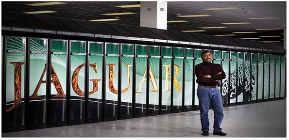
As of July 2011,
the computer showed a peak seed of 2.33 petaflops (2.33·1015 floating point
operations per second), and a sustained performance in excess of 1.0 petaflop. The upgraded system has an 84–cabinet Cray
XT4 and a200–cabinet upgraded Cray XT5.
Each XT4 has 8 gigabytes per node, and each XT5 has 16 gigabytes per
node, for a total of 362 terabytes of high speed memory. The total processor count is 37,376 six–core
AMD Opterons (in the XT5) and 7,832 quad–core AMD Opterons (in the XT4). The XT4 part of the system is air cooled, but
the XT5 part must be liquid cooled, using the commercial refrigerant R–134. The Jaguar requires 12.7 megawatts of
electric power and a continuous supply of chilled air and refrigerant.
In every sense of the word, this is a big computer.