An Extended (Silly) Example of I/O Strategies
There are four
major strategies that can be applied to management of the I/O process:
Program-Controlled, and
Interrupt-Driven, and
Direct Memory Access, and
I/O Channel.
We try to clarify the difference between these strategies by the example of having a party in one’s house to which guests are invited. The issue here is balancing work done in the house to prepare it for the party with the tasks of waiting at the front door to admit the guests.
Program-Controlled
The analogy for
program-controlled I/O would be for the host to remain at the door, constantly
looking out, and admitting guests as each one arrives. The host would be at the door constantly
until the proper number of guests arrived, at which time he or she could continue
preparations for the party. While
standing at the door, the host could do no other productive work. Most of us would consider that a waste of
time.
Interrupt-Driven
Many of us have
solved this problem by use of an interrupt mechanism called a doorbell. When the doorbell rings, the host suspends
the current task and answers the door.
Having admitted the guest, the host can then return to preparations for
the party. Note that this example
contains, by implication, several issues associated with interrupt handling.
The first issue is priority. If the host
is in the process of putting out a fire in the kitchen, he or she may not
answer the door until the fire is suppressed.
A related issue is necessary completion.
If the host has just taken a cake out of the oven, he or she will not
drop the cake on the floor to answer the door, but will first put the cake down
on a safe place and then proceed to the door.
In this scenario, the host’s time is spent more efficiently as he or she
spends little time actually attending the door and can spend most of the time
in productive work on the party.
Direct Memory Access
In this case, the
host unlocks the door and places a note on it indicating that the guests should
just open the door and come in. The host
places a number of tickets at the door, one for each guest expected, with a
note that the guest taking the last ticket should so inform the host. When the guest taking the last ticket has
arrived, the host is notified and locks the door. In this example the host’s work is minimized
by removing the requirement to go to the door for each arrival of a guest. There are only two trips to the door, one at
the beginning to set up for the arrival of guests and one at the end to close
the door.
I/O Channel
The host hires a
butler to attend the door and lets the butler decide the best way to do
it. The butler is expected to announce
when all the guests have arrived.
Note that the I/O channel is not really a distinct strategy. Within the context of our silly example, we note that the butler will use one of the above three strategies to admit guests. The point of the strategy in this context is that the host is relieved of the duties. In the real world of computer I/O, the central processor is relieved of most I/O management duties.
I/O Device Registers
From the viewpoint of the CPU, each I/O device is nothing more than a
set of registers. An Input device is
characterized by its input Data register from which the CPU reads data. An Output device is likewise characterized by
its data register.
For the Boz–7, we shall use a somewhat unusual design with 32–bit registers. Each I/O device will have four 32–bit registers.
Data used for data to be read from or
written to the I/O device
for input
devices this is a read-only register
for output
devices this register is usually nor read by the CPU
Status used to report the device
status. If the sign bit (bit 31) is 1,
there
has been a
device error. The assignment of bit 31
as an overall
error bit
(other bits for specific errors) is for ease of programming, as a
status register
with the error bit set will be read as a negative number.
Control used to set options on the I/O device
Disk drives
have control registers to select cylinder, track, sector, etc.
Extra four registers per device simplifies
the address calculations.
In these
designs, we shall ignore the Extra register.
The Boz–7
allocates 216 (65,536) addresses for I/O registers. We have specified that each I/O device has
four addressable registers, so the maximum number of I/O devices is easily
calculated at 65,536 / 4 = 16,384. We
postulate a design that allows for 16,384 I/O devices. We specify that the addresses for each I/O
device are a multiple of four. For an
I/O device with data register address N, we specify the following:
N the
address of the data register
N + 1 the address of the status register
N + 2 the address of the control register
N + 3 the address of the “extra” register (no real designs have
such a register).
Note that
for device K (0 £
K £
16383) that N = 4·K,
so that the address of the data register of the I/O device is always a multiple
of four. Thus, for device K, we have the
following:
4·K the address of the data register
4·K + 1 the address of the status register
4·K + 2 the address of the control register
4·K + 3 the address of the “extra” register.
With this definition, we can split the 12-bit I/O register address into two parts.
|
Bit |
15 |
14 |
13 |
12 |
11 |
10 |
9 |
8 |
7 |
6 |
5 |
4 |
3 |
2 |
1 |
0 |
|
|
I/O Device number |
Register Type |
||||||||||||||
We should make an immediate disclaimer at this point. No serious computer design would contemplate actually having 16,384 I/O devices attached. Here we follow the common practice of providing a wide number of I/O “ports” for a wide variety of potential I/O device types with the expectation that fewer than 100 I/O devices will actually be used.
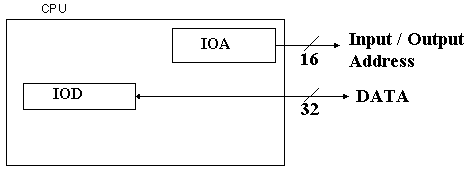
General I/O Structure
We first
consider the revised method for connecting the CPU to the I/O device. This design uses two registers:
IOA a
16–bit I/O Address Register, and
IOD a
32–bit I/O Data Register.
In isolated I/O, the I/O system has address and data buses that are distinct from the address and data buses used for the memory. We postulate a 16–bit I/O address bus connected to the IOA register in the CPU (see below) and a 32–bit I/O Data bus that is connected to the IOD register. This overall structure is shown in the following figure.
Each device is connected by an Interface Unit, the purpose of which is to determine if the specific I/O device is being addressed by the CPU and to handle the data and status/control information transactions in the case that the device is being addressed.
The next figure shows a top-level description of the I/O device interface unit.
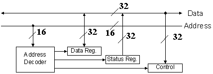
The purpose of the Address Decoder is to determine if the address on the I/O Address Lines corresponds to one of the four registers associated with the I/O device. Only three of these registers are shown in the figure: Data, Status, and Control.
If the device’s data register is being addressed, then the data are copied from the data register to the I/O data lines for a LDR or from the I/O data lines to the data register for STR. If the device’s status register is being addressed, then the status data are copied from the status register to the I/O data lines; this in response to a LDR instruction. If the device’s control register is being addressed, then the control data are copied from the I/O data lines to the device’s control register; this in response to a STR instruction.
We now investigate
the details of the I/O device’s address decoder. In our design, the I/O address is an 16 bit
address; thus I/O addresses are in the range 0 to 16383 inclusive. We have further specified that the address of
the I/O device’s data register is a multiple of four and that for N = 4·K (0 £ K £ 16383)
as an I/O address that
N is
the address of the data register
N + 1 is the address of the status register
N + 2 is the address of the control register
N + 3 is the address of the extra register (not shown in any of
the figures)
The implication of this design is that the high order 14 bits (A15-2) of the I/O address lines (A15-0) select the I/O device and that the low order two bits (A1-0) select the register within the I/O device. The following table restates the above. For each I/O device/
|
A1 |
A0 |
Register |
|
0 |
0 |
Data |
|
0 |
1 |
Status |
|
1 |
0 |
Control |
|
1 |
1 |
Extra (not shown) |
The next figure shows how the I/O address decoder functions. When an I/O device is attached to the I/O bus, its address is fixed by setting a number of jumper switches to 0 and 1. The reader will note that the figure is drawn for an eight–bit address bus, though the idea scales quite easily. We have elected the simpler I/O structure to avoid a very messy figure.
This figure shows an address decoder set to 101110, for device number 46. As 46·4 = 184, the addresses for this device are 184 for the data register, 185 for the status register, 186 for the control register, and 187 for the extra register.
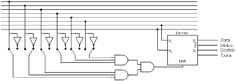
Figure: Address Decoder for An Eight–Bit I/O Address
Note that each line in the address bus is connected to the corresponding line of the I/O address decoder either directly or through an inverter. The connection selected is determined by the jumper switch. In the figure, the jumper switches are shown using the diagonal lines. Note also that the 6–input AND gate is fabricated from two 3–input AND gates and a 2–input AND gate; this being just a reminder that logic gates have an upper limit to input count.
When the device is selected (the upper bits of the IOA being set to 101110), the 2–to–4 decoder is enabled and the lower two bits of the IOA select an I/O register associated with the device. When the device is not selected, its address decoder is disabled.
The First Idea, and Why It Cannot Work
At first
consideration, I/O in a computer system would appear trivial. We just issue the instructions and access the
data register by address, so that we have:
GET %R7 TEXT_IN_DATA -- this reads from the input unit.
PUT %R2 TEXT_OUT_DATA -- this writes to the output unit.
Strictly speaking, these instructions operate as advertised in the code fragments above. We now expose the difficulties, beginning with the input problem. The input unit is connected to the CPU through the register at address TEXT_IN_DATA. Loading a CPU from that input register will always transfer some data, but might not transfer what we want. Normally, we expect an input request to wait until a character has been input by the user and only then transfer the character to the CPU. As written above, the instruction just copies what is in the data buffer of the input unit; it might be user data or it might be garbage left over from initialization. We must find a way to command the unit to read, wait for a new character to have been input, and only then transfer the data to the CPU.
The output instruction listed above might as well be stated as “Just throw it over the wall and hope someone catches it.” We are sending data to the output unit without first testing to see if the output unit is ready for data. Early in his career as a programmer, this author wrote a program that sent characters to a teletype printer faster than they could be printed; the result was that each character printed was a combination of two or more characters actually sent to the TTY, and none were actually correct. As this was the intended result of this experiment, this author was pleased and determined that he had learned something.
The solution to the problem of actually being able to do input and output correctly is based on the proper use of these two instructions. The solution we shall describe is called program controlled I/O. We shall first describe the method and then note its shortcomings.
Program Controlled I/O
The basic idea for program-controlled I/O is that the CPU initiates all input and output operations. The CPU must test the status of each device before attempting to use it and issue an I/O command only when the device is ready to accept the command. The CPU then commands the device and continually checks the device status until it detects that the device is ready for an I/O event. For input, this happens when the device has new data in its data buffer. For output, this happens when the device is ready to accept new data.
A Code Fragment for Input
Here is a
code fragment that indicates what must be done to read a character from the
input unit. The code fragment uses the
following constants and addresses. TEXT_IN_STATUS the address of the status register for the
device.
TEXT_IN_ERROR the address of an error handler for this device. We show
this to emphasize the
possibility of device errors and
highlight the need to
handle errors, but do not further
define the error
handling code, which can be complex.
READ_A_CHAR A
numeric constant that sets the bits in the device’s
command register that
will cause it to read a character.
TEXT_IN_COMMAND the address of the command
register for the device.
TEXT_IN_DATA the address of the data register for the device.
The Input Code Fragment
B1: GET %R1, TEXT_IN_STATUS //Read
the device status
TST %R1 //Check its sign
BNS TEXT_IN_ERROR //If negative, we have an
//error
and must handle.
BGT B1 //If positive, device busy
LDI %R2, READ_A_CHAR //Load
constant to command a
PUT %R2, TEXT_IN_COMMAND //read
and send this value to
//the
device control register
B2: GET %R1, TEXT_IN_STATUS //Check the device status
TST %R1 //continually to detect that
the
BNS TEXT_IN_ERROR //read has been completed.
BGT B2 //Device busy – no input
yet.
GET %R3, TEXT_IN_DATA //Now
get the character input.
A Code Fragment for Output
B3: GET %R1, TEXT_OUT_STATUS //Read
the device status
TST %R1 //Check its sign
BNS TEXT_OUT_ERROR //Handle the error if necessary
BGT B3 //If positive, device busy
LDR %R3, DATA_MEM_LOC //Get the char from memory
PUT %R3, TEXT_OUT_DATA //Place
it in the data buffer
LDI %R2, WRITE_A_CHAR //Load
constant to command a
PUT %R2, TEXT_OUT_COMMAND //write and send this value to
//the
device control register.
The Busy Wait
Program-controlled I/O is the simplest form of I/O processing. As such, it is expected to have some problems, most noticeably the “busy wait” in which the CPU executes a tight loop doing nothing except waiting for the I/O device to complete its transaction. The shortcomings of such a method are obvious (IBM had observed them in the late 1940’s) and cluster on two major issues.
Designs to Avoid the Busy Wait
As a result of the imbalance in the timings of the purely electronic CPU and the electro-mechanical I/O devices, a number of I/O strategies have evolved. We shall discuss these in this chapter. All modern methods move away from the designs that cause the CPU to be the only component to initiate I/O.
The idea of involving the CPU in an I/O operation only when the operation can be executed immediately is the basis of what is called interrupt-driven I/O. In such cases, the CPU manages the I/O but does not waste time waiting on busy I/O devices. There is another strategy in which the CPU turns over management of the I/O process to the I/O device itself. In this strategy, called direct memory access or DMA, the CPU is interrupted only at the start and termination of the I/O. When the I/O device issues an interrupt indicating that I/O may proceed, the CPU issues instructions enabling the I/O device to manage the transfer and interrupt the CPU upon normal termination of I/O or the occurrence of errors.
The Device
Interrupt
Up to this point, we have investigated how the CPU interacts with the I/O device by placing its register addresses on the address lines and placing or retrieving data from the data lines. We now investigate the method for the I/O device generating an interrupt, which is an asynchronous signal to the CPU. To do this, the I/O device is connected to an interrupt line, which it drives either high (logic 1) or low (logic 0) to indicate an interrupt. The CPU, or the interrupt controller acting for the CPU, will then acknowledge the interrupt.
Another term for generating an interrupt is “raising” an interrupt.
Here is the
scenario for an interrupt for an input device:
1) The
device raises an interrupt when it has new data for input.
2) The
CPU or Interrupt Controller sends an ACK to the device, as yet not fully
identified, along the ACK line
associated with the incoming INT.
3) The
I/O device identifies itself to the CPU.
4) If
the priority is proper, the interrupt is handled.
As an immediate consequence of allowing interrupts, we see that the bus must include not only data and address lines, but also interrupt and acknowledge lines. In a multi-priority data bus, each level of priority must have its own interrupt and acknowledge lines.
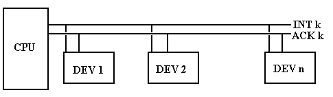
The design for the Boz–7 calls for the interrupt lines to be asserted low, that is that the I/O device asserts an interrupt by driving the line to zero voltage (logic 0). This scheme allows for multiple devices to use the same interrupt line, as shown in the figure below.
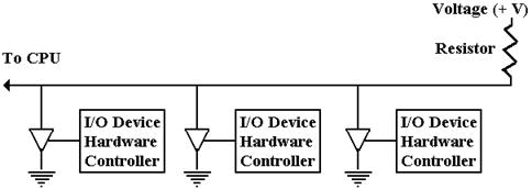
In the figure we see the controllers for three I/O devices attached to an interrupt line. As long as none of the tri-state buffers are enabled, the voltage source keeps the line at logic 1. When one or more of the tri-state buffers is activated, the voltage in the interrupt line drops to zero (logic 0) and an interrupt is signaled. More than one can interrupt at the same time.
This design, in which the interrupts are asserted low and the acknowledgement signals are asserted high, follows the design of the PDP–11 manufactured by the Digital Equipment Corporation. DEC is now out of business, but its computers were examples of good design practices and for that reason this text adopts their I/O structure.
A Structure for Interrupts
We now design an I/O structure based on assignment of priority levels to I/O devices. We follow the PDP-11 strategy of an eight-level priority scheme, with priorities from 0 through 7 inclusive. In this scheme, priority levels 4 through 7 are assigned to hardware interrupts and priorities 0 through 3 are assigned to software interrupts (not studied here).
The first step in handling interrupts is for the CPU to be signaled that there is an interrupt. Once the CPU has received an interrupt signal (denoted as INT in the figure below), it generates an acknowledge signal or ACK. This figure shows the interrupt handling.
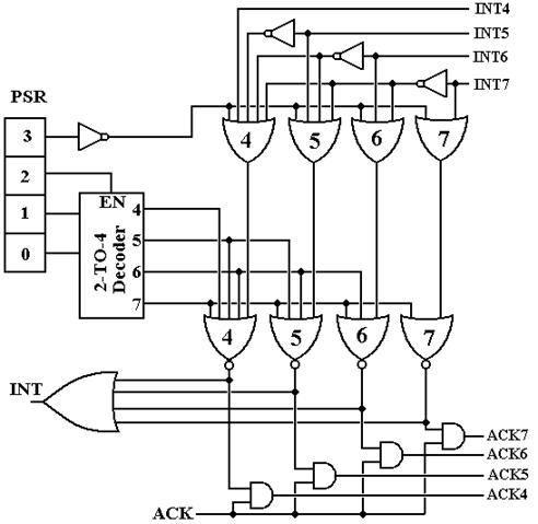
Interrupt Handler for the Boz–7
In this structure, the device interrupts are only at levels 4 through 7, with higher numbered interrupts being more urgent than lower numbered ones. Thus, one might assign level 4 to the keyboard and level 7 to a disk drive, which has to be serviced more quickly.
The purpose of this circuit is to generate a single signal INT to the CPU and issue an ACK at exactly one of the levels when the CPU asserts ACK.
It would be helpful to view this circuit one level at a time, beginning with the top layer of OR gates that controls which interrupt, if any, gets processed. At this stage, the interrupts are active low, so that an interrupt is “raised” by placing a logic 0 on the line. The goal of this stage of the circuit is to output no more than a single 0 only when interrupts are enabled. When interrupts are enabled, the OR gate associated with the highest priority interrupt outputs a logic 0, and all other OR gates output a logic 1.
Bit 3 of the PSR is the I-bit or Interrupt-Enabled bit. If the I–bit is 0, interrupts are disabled and the CPU will not acknowledge an interrupt. Note that, in this row of OR gates, each gate has the negation of bit 3 of the PSR as an input. When bit 3 of the PSR is 0, all these OR gates output 1, and no interrupt is passed to the processing circuitry. When bit 3 of the PSR is 1, its negation is 0 and it does not affect the output of these four OR gates.
The next thing to notice is the circuitry to insure that only one interrupt at a time is processed. This is an adaptation of the Multiple-Match Resolver seen in Associative Memory. Here, the presence of any interrupt suppresses an interrupt of lower level. For example, if INT7 = 0, then the outputs of OR gates 4, 5, and 6 will be 1 without regard to the value of INT4, INT5, or INT6. Likewise, if INT7 = 1 and INT6 =0, then the output of OR gate 7 will be 1 because INT7 = 1, the outputs of gates 4 and 5 will be 1 without regard to the value of INT4 or INT5, and the output of OR gate 6 will depend on bit 3 of the PSR.
The goal of this part of the circuitry is to allow at most one interrupt at a time to generate a signal to the CPU and cause an interrupt handler to execute. We use this logic to prioritize interrupts, but must remember that an improper design can lead to low-priority interrupts never being served. This problem is called “indefinite postponement”, and is studied extensively in courses on Operating Systems.
As an aside
we mention what can happen if the devices are not allocated correctly to the
four priority levels available. What can
happen is that a device is always eligible to have its interrupt acknowledged,
but never gets the ACK. Consider the
following scenario.
1) A
device at priority level 7 interrupts, and
2) Before
this device is handled, a device at priority level 6 interrupts, and
3) When
the level 7 priority device is handled, the level 6 handler begins, and
4) Before
the level 6 device is handled, the level 7 device again interrupts, etc.
Any two high priority devices can “hog” the CPU, preventing a lower priority device from ever being serviced. This is one of the problems facing an I/O designer.
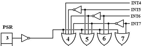
Consider now the “middle part” of this circuit. Its job is to compare the running priority of the CPU against the priority of the interrupt and process the interrupt only if its priority is higher than the CPU priority.
If the running priority of the CPU is less than 4, then IR2 = 0 and the 2-to-4 decoder is disabled, having all of its outputs equal to 0. When this occurs, all four NOR gates at the bottom of this figure are passed through and any interrupt is processed. If the running priority of the CPU is greater than 3, then the 2-to-4 decoder is active and one of its outputs (the one corresponding to the running priority of the CPU) is active. Note that an output at a given level causes the outputs of NOR gates at an equal or lower level to be 0. Thus, if the CPU is running at priority 7 (presumably because it is handling a priority 7 interrupt), then the outputs of all NOR gates at the bottom of the figure will be 0. Similarly, if the CPU is running at priority level 5, the outputs of NOR gates 4 and 5 will be 0, and either or both of the outputs of NOR gate 6 or 7 will be zero (a maximum of one of these 2 outputs can be 1).
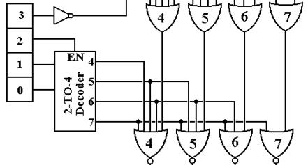
The final part of this circuit shows how the signal INT to the CPU is generated and the signal ACK from the CPU is handled to be distributed to the proper I/O device. At this point, we should understand the role of the CPU vs. the role of the interrupt circuitry in this game.
1) The interrupt handler
circuitry determines if an interrupt can be sent to the CPU.
2) If
an interrupt is proper, the interrupt handler raises an INT to the CPU.
3) The
CPU suspends processing when it can and asserts an ACK
4) The
interrupt handler passes the ACK to the proper acknowledge line.
We shall see shortly how the interrupting device captures the ACK and identifies itself to the CPU, but at the moment, we need to focus on the last piece of this circuit.
The final piece of the circuit deals with asserting an INT to the CPU and processing the ACK when the CPU asserts that signal. The main thing to note here is that the interrupting device continues to assert its interrupt until it receives an acknowledgement.
At this point, we assume that the output of exactly one of the NOR gates at the top of the figure is 1. We have developed the circuitry to prevent the output of more than one of the gates being 1. If the output of all of the NOR gates is 0, nothing happens.
The signal INT is generated when there are interrupts at any level. This is the one signal to the CPU that there has been an interrupt, which is to be handled. The CPU suspends the active process and prepares to process the new interrupt. When the CPU is ready to process the interrupt it generates an ACK signal. At this point in time, the interrupting device is still asserting its interrupt and so the output of exactly one of the NOR gates at the top of the figure is 1 and the ACK causes exactly one of the ACK lines output to the devices to be 1.
Daisy-Chaining
We have postulated an I/O architecture with four levels of interrupts. Were we to restrict our design to four I/O devices, one at each priority level, we would have a simple design that would be of very little use. All practical I/O designs must allow for more than one I/O device per priority line.
The question then arises of how to assign relative priority to devices that interrupt on the same priority level. The answer is a method, called “daisy chaining” that handles the distribution of the acknowledge signal for that interrupt level. There is a “pecking order” based on physical proximity to the CPU that determines which of the devices with the same priority gets the ACK first and thus responds. This design is called “daisy chaining”.
Again, we need to worry about placing too many devices on a single priority level so that we can avoid indefinite postponement of a device that it physically remote from the CPU.
The daisy chain concept describes the handling of the ACK signal at the given priority level. Thus, if we are handling priority 6 devices, it is ACK6 that we are concerned with.
At the top level, we consider a number of devices attached to a given interrupt line and its corresponding acknowledge line.
What we mean by “physical proximity” to the CPU is that a device closer to the CPU processes a signal and passes it to a device further from the CPU. In the example above, device 2 gets the ACK signal only after device 1 has processed it. In processing the ACK signal, device 1 can “capture” it or just pass it on to the next device in the daisy chain.
The next figure shows the details of the daisy chain for one I/O device of priority level 5. In this, as in the above, the CPU is to the left and the next device to the right.
Individual I/O Device Placed in the Daisy
Chain
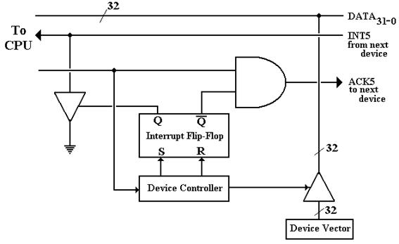
The sequence of events for a device raising and handling an interrupt is as follows.
1) The device controller
sets the device’s interrupt flip-flop.
This causes a
signal to be asserted on the
appropriate interrupt line, here INT5.
2) The interrupt handler
circuit is here assumed to pass the interrupt to the CPU
by asserting the INT signal to
the CPU.
3) The
CPU returns an ACK to the interrupt handler circuit, which asserts ACK5.
4) The ACK signal is
sent to the I/O device controller. Note
that when the ACK
signal arrives at the
controller, that its interrupt flip-flop is set, so that the
AND gate on the ACK line
prevents the ACK signal from propagating to the
device next in the daisy
chain.
5) The I/O device
controller places a 32–bit vector on the I/O data lines. Details
of this vector are discussed
just below in the topic on vectored interrupts.
6) The I/O device controller resets its interrupt flip-flop.
Vectored Interrupts
At this point, all that has happened is that a device has interrupted and been acknowledged. We now ask the question of how to process the I/O for the device. There are a number of ways by which the I/O device can identify itself to the CPU and cause its device handler to be run. We focus on one simple method that is used by many computers – the device sends its vector on the data lines.
A vector is an address in memory associated with the device. The most common usage is that the vector be
the address of a pointer to the device handler; thus the operative code would
be
BRU *DEVICE_VECTOR
This removes the requirement for the designer of the I/O device and the designer of the operating system to agree on the address of the code to handle the I/O device. All that is needed is to agree on a single slot sufficient to hold an address. When the operating system is loaded, the loader places the device handler at any address that is best and places the address of the handler in the agreed location, with address corresponding to the device vector. The pointers to I/O routines are often stored in low memory.
In many Intel-based computers, the address of the handler is a 20–bit address stored in the form of Segment:Offset. Remember that this format stores a 20–bit address in two parts – a 16-bit segment and a 16-bit offset; the address is formed by (Segment · 16) + Offset. The student should also recall that Intel uses the term IP (Instruction Pointer) for our PC.
Vectored Interrupts and
IRQ’s
The main issue associated with the handling of interrupts is the address of the routine to be associated with handling the interrupt. One of the common methods uses a vector, which is the address of a location containing the address of the routine. In C++ terminology, the vector is the address of a pointer to the routine.
Connecting a new I/O device to a computer is a process involving at least two steps.
1) Connecting the device
to the I/O bus.
2) Installing
the software to handle the device.
The use of the device vector as the address of a pointer to the handler software is explained by supposing that the vector is the address of the handler itself. Under this latter hypothesis, the device developer and the software developer would have to agree on a fixed address for the software to handle the device – an extremely rigid constraint.
The pointer solution used with vectored interrupts allows much greater flexibility in the development of software. The device developer and operating system developer must agree only on a location in memory to contain the address of the handler routine. When that routine is loaded into memory, the loader copies its address into the fixed address.
When running under DOS (and presumably Windows) the PC allocates the lower 1024 bytes of memory (at addresses 0 – 1023 or 0 – 0x3FF) to the interrupt vector table, which is an array of 256 addresses in the form segment:offset. Recalling that each of the segment and offset addresses is 16 bits, we see that 32 bits or 4 bytes are devoted to each of the pointers in the table (they are far pointers) and thus the table contains 1024 / 4 = 256 addresses.
The Intel 8088 and 80x86 series are all byte–addressable machines. As an immediate result, all 16-bit words are to be found at even addresses and all 32–bit double words are at addresses that are multiples of 4. For 0 £ I £ 255, let I be the interrupt number.
Then address 4·I contains
the IP (Instruction Pointer) for the handler routine
address 4·I + 2 contains the CS (Code Segment) for
the handler routine
The process of handling an
interrupt is basically as follows.
1) The
interrupting device asserts its vector on the I/O bus.
The vector is the address of
the 16-bit word containing the IP for its handler.
2) The
generic interrupt handler retrieves the IP and CS from the specified addresses.
These are formed into an
address CS:IP used to locate the I/O handler.
3) The
handler at that 20-bit address is executed and the interrupt is handled.
Of course, there is a lot more to interrupt handling that what we have discussed. The most noticeable omission is a provision for saving the context of an interrupted program. The basic idea is that the process that was interrupted must be able to resume execution after the interrupt with the same state as it had before the interrupt. Saving the contents of RAM does not present a problem as the interrupt handler references different addresses. It is the register contents that must be saved. For the ASC, this includes the PC, ACC, and index registers.
Returning to the PC/AT (with an Intel 80286 chip), we list the first 16 entries in the interrupt vector table. Future editions of these notes will reference the Pentium map.
Interrupt Address Purpose
Number (Hex)
0 0000 Processor:
Division by zero
1 0004 Processor:
Single Step
2 0008 Processor:
Error in RAM chip
3 000C Processor:
Breakpoint reached
4 0010 Processor:
Numeric Overflow
5 0014 Hardcopy
(whatever that is)
6 0018 80286
only: Unknown instruction
7 001C Reserved
(used by DOS for an undocumented function)
8 0020 IRQ0 Timer
9 0024 IRQ1 Keyboard
A 0028 IRQ2
B 002C IRQ3 Serial Port 2
C 0030 IRQ4 Serial Port 1
D 0034 IRQ5 Hard Drive
E 0038 IRQ6 Diskette
F 003C IRQ7 Printer
The Intel 8259 is a support chip used to handle interrupts and generate the vectors needed by DOS to access the device handler. Each 8259 can process up to eight IRQ’s (Interrupt Requests) simultaneously. The support chip we are examining handles IRQ0 through IRQ7 and is assigned interrupts 8 through F in the interrupt vector table.
The Intel 8259 imposes a priority ordering on the interrupts. The device associated with IRQ0 has the highest priority, followed by the device on IRQ1, etc. Should two devices signal the 8259 at the same time, it passes the vector associated with the higher priority (lower IRQ number) device to the CPU interrupt handler.
Suppose that we have the
following memory map when IRQ1 is raised.
0024 0x0200
0026 0x3000
1) The Intel 8259
support chip asserts interrupt vector 0024 on the I/O bus.
2) The
CPU interrupt handler finds the segment and offset for the handler
routine at the table address
given by the vector
3) The 20-bit address
0x3000 ·
0x10 + 0x0200 = 0x30000 + 0x0200 = 0x30200
is formed and execution begins
at that address.
Direct Memory Access (DMA)
In order to consider the next refinement of the I/O structure, let us consider what we have discussed previously. Suppose that a line of 80 typed characters is to be input.
Program Control
In this model, the CPU first tests the status of the input unit and does nothing else until the first character is input. After that, it does nothing except input the 80 characters for the approximately 8 to 16 seconds during which the characters are being input.
Interrupt Driven
Here the CPU suspends the program that requests the Input and activates another process. While this other process is being executed, the input device raises 80 interrupts, one for each of the characters input. When the interrupt is raised, the device handler is activated for the very short time that it takes to copy the character into a buffer, and then the other process is activated again. When the input is complete, the original user process is resumed.
Direct Memory Access
DMA is a refinement of interrupt-driven I/O in that it uses interrupts at the beginning and end of the I/O, but not during the transfer of data. The implication here is that the actual transfer of data is not handled by the CPU (which would do that by processing interrupts), but by the I/O controller itself. This removes a considerable burden from the CPU.
In the DMA scenario, the CPU suspends the program that requests the input and again activates another process that is eligible to execute. When the I/O device raises an interrupt indicating that it is ready to start I/O, the other process is suspended and an I/O process begins. The purpose of this I/O process is to initiate the device I/O, after which the other process is resumed. There is no interrupt again until the I/O is finished.
DMA Controller
Any I/O device controller is a sequential circuit that connects an I/O device to the system bus. A DMA controller is a limited-capability processor that can transfer data to and from main memory. As a result of this, it must be able to access the Memory Access Register (MAR) and the Memory Buffer Register (MBR) of the main memory.
Immediately, we see the need for a bus arbitration strategy – suppose that both the CPU and a DMA controller want to access the memory at the same time. The solution to this problem is called “cycle stealing”, in which the CPU is blocked for a cycle from accessing the memory in order to give preference to the DMA device.
Any DMA controller must contain at least four registers used to interface to the system bus.
1) A word count register
(WCR) – indicating how many words to transfer.
2) An
address register (AR) – indicating the memory address to be used.
3) A
data buffer.
4) A
status register, to allow the device status to be tested by the CPU.
The basic operation of the DMA controller is described as follows.
When the I/O is initiated
1) The
CPU tests the status of the device, using its status register.
2) The
CPU loads the AR with the starting address for the I/O.
3) The
CPU loads the WCR with the number of items expected for the transfer.
When the DMA device manages the
I/O, the CPU continues other processing, and
1) For
every transfer the WCR is decremented.
2) For
every transfer the AR is incremented.
When the I/O process is complete, the DMA device raises an interrupt and the CPU activates a process to handle the termination of I/O.
The figure below shows the essential structure of the DMA controller and its interaction with the main memory through the system bus.
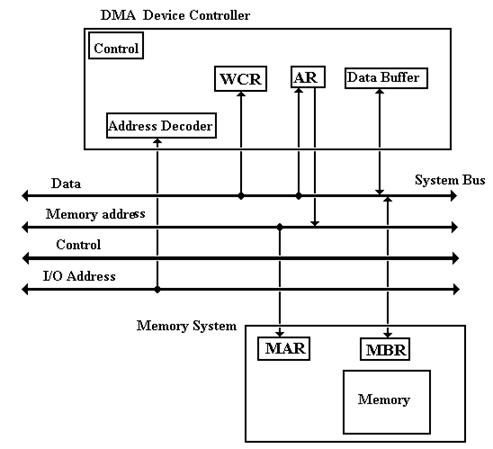
DMA Transfer Structure
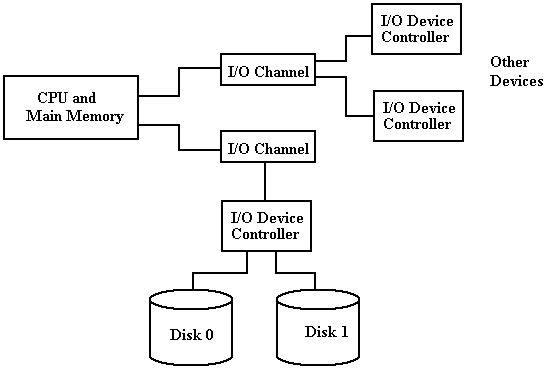
I/O Channel
A channel is a separate special-purpose computer that serves as a sophisticated Direct Memory Access device controller. It directs data between a number of I/O devices and the main memory of the computer. Generally, the difference is that a DMA controller will handle only one device, while an I/O channel will handle a number of devices.
The I/O channel concept was developed by IBM (the International Business Machine Corporation) in the 1940’s because it was obvious even then that data Input/Output might be a real limit on computer performance if the I/O controller were poorly designed. By the IBM naming convention, I/O channels execute channel commands, as opposed to instructions.
There are two types of channels
– multiplexer and selector.
A multiplexer channel supports more
than one I/O device by interleaving the transfer of blocks of data. A byte
multiplexer channel will be used to handle a number of low-speed devices,
such as printers and terminals. A block multiplexer channel is used to
support higher-speed devices, such as tape drives and disks.
A selector channel is designed to handle high speed devices, one at a time. This type of channel became largely disused prior to 1980, probably replaced by blocked multiplexers.
Each I/O channel is attached to one or more I/O devices through device controllers that are similar to those used for Interrupt-Driven I/O and DMA, as discussed above.
I/O Channels, Control Units, and I/O
Devices
In one sense, an I/O channel is not really a distinct I/O strategy, due to the fact that an I/O channel is a special purpose processor that uses either Interrupt-Driven I/O or DMA to affect its I/O done on behalf of the central processor. This view is unnecessarily academic.
In the IBM System-370 architecture, the CPU initiates I/O by executing a specific instruction in the CPU instruction set: EXCP for Execute Channel Program. Channel programs are essentially one word programs that can be “chained” to form multi-command sequences.
Physical IOCS
The low level programming of I/O channels, called PIOCS for Physical I/O Control System, provides for channel scheduling, error recovery, and interrupt handling. At this level, the one writes a channel program (one or more channel command words) and synchronizes the main program with the completion of I/O operations. For example, consider double-buffered I/O, in which a data buffer is filled and then processed while another data buffer is being filled. It is very important to verify that the buffer has been filled prior to processing the data in it.
In the IBM PIOCS there are four major macros used to write the code.
CCW Channel Command Word
The CCW macro causes the IBM assembler to construct an 8-byte channel command word. The CCW includes the I/O command code (1 for read, 2 for write, and other values), the start address in main memory for the I/O transfer, a number of flag bits, and a count field.
EXCP Execute Channel Program
This macro causes the physical I/O system to start an I/O operation. This macro takes as its single argument the address of a block of channel commands to be executed.
WAIT
This synchronizes main program execution with the completion of an I/O operation. This macro takes as its single argument the address of the block of channel commands for which it will wait.
Chaining
The PIOCS provides a number of interesting chaining options, including command chaining. By default, a channel program comprises only one channel command word. To execute more than one channel command word before terminating the I/O operation, it is necessary to chain each command word to the next one in the sequence; only the last command word in the block does not contain a chain bit.
Here is a sample of I/O code.
The main I/O code is as follows. Note that the program waits for I/O completion.
// First execute the channel program at
address INDEVICE.
EXCP INDEVICE
// Then wait to synchronize program
execution with the I/O
WAIT INDEVICE
// Fill three arrays in sequence, each with
100 bytes.
INDEVICE CCW 2, ARRAY_A, X’40’, 100
CCW 2, ARRAY_B, X’40’, 100
CCW 2, ARRAY_C, X’00’, 100
The first number in the CCW (channel command word) is the command code indicating the operation to be performed; e.g., 1 for write and 2 for read. The hexadecimal 40 in the CCW is the “chain command flag” indicating that the commands should be chained. Note that the last command in the list has a chain command flag set to 0, indicating that it is the last one.
One way to view an I/O channel and channel programming is to view the channel program as a set of orders sent by the CPU to the channel – “Here do this and tell me when you’re done”.
Front End Processor
We can push the I/O design strategy one step further – let another computer handle it. One example that used to be common occurred when the IBM 7090 was introduced. At the time, the IBM 1400 series computer was quite popular. The IBM 7090 was designed to facilitate scientific computations and was very good at that, but it was not very good at I/O processing. As the IBM 1400 series excelled at I/O processing it was often used as an I/O front-end processor, allowing the IBM 7090 to handle I/O only via tape drives.
The batch scenario worked as
follows:
1) Jobs
to be executed were “batched” via the IBM 1401 onto magnetic tape. This
scenario did not support time
sharing.
2) The
IBM 7090 read the tapes, processed the jobs, and wrote results to tape.
3) The
IBM 1401 read the tape and output the results as indicated. This output
included program listings and
any data output required.
Another system that was in use was a combined CDC 6400/CDC7600 system (with computers made by Control Data Corporation), in which the CDC 6400 operated as an I/O front-end and wrote to disk files for processing by the CDC 7600. This combination was in addition to the fact that each of the CDC 6400 and CDC 7600 had a number of IOPS (I/O Processors) that were essentially I/O channels as defined by IBM.
Note the terminology here. One could easily consider a Front End Processor to be a specialized I/O channel. There is no reason not to do so.
Computer Networks: I/O Considerations
The study of computer networks is quite fascinating and important. There are a number of security issues associated with network use that demand attention from anyone who is a serious user of computers that are networked. For the purposes of this text, we examine how a typical computer is connected to the network, and the I/O process for that connection equipment to communicate with the computer’s CPU and memory. Much of this material is based on two books by Douglas E. Comer [R102, R103].
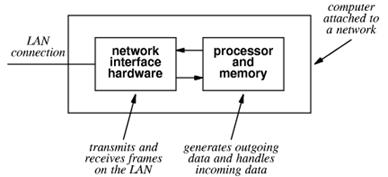
We consider our computers to be connected to the Internet. Technically, it is the NIC (Network Interface Card) that is connected.
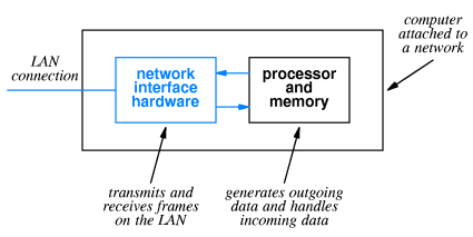
The Network Interface Card is an Input / Output device attached to the computer. The NIC handles many of the tasks related to communicating with the LAN (Local Area Network) to which the computer, through the NIC, is connected. Each NIC has a unique physical network address, called MAC address (for Media Access Control) address, which is a 48–bit address that identifies the NIC, not the computer. Some computers, such as those designed to be routers, have more than one NIC. We shall not consider those in this chapter.
From the view of the computer, the NIC is a DMA device that is an I/O intermediary between the computer and the Global Internet. We now discuss how to attach a typical computer, or really its NIC, to a local area network.
Attaching a Computer to a Network
This is a typical attachment that uses the original (Thicknet) wiring.
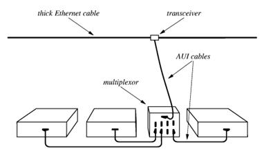
A number of devices in a single room would be connected through a multiplexor to the cable (called an “Ethernet cable”, after its protocol) through a transceiver (called an “AUI” for “Attachment Unit Interface”). The AUI was typically placed above a false ceiling, making it hard to locate and repair a malfunctioning unit. Your author has been, on occasion, required to work above a false ceiling; it is not much fun.
Current technology for attaching computers to a network uses a technology called twisted pair wiring. Names for this wiring include “10BaseT” and “100BaseT”. The twisted pair cable attaches to the NIC through a RJ–45 connector.
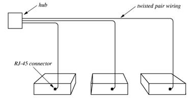
The hub connects these computers to the larger network. The mathematicians will note that this hub and computer arrangement is a star topology with the hub at the center, and not the expected ring topology, supposedly used for networks. Each network segment of this type is treated logically as if it were a ring, even though it is not.
Here is a typical group setup in which a number of computers are connected to the Internet through a hub. The hub is often contained in a “network closet”, which is a small locked room. This facilitates maintaining and securing the network assets.
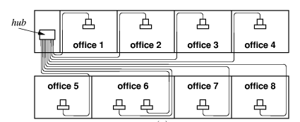
The only part of the network above the ceiling is a collection of twisted–pair wires, which are usually quite reliable. In any case they are easy and cheap to replace. In an initial wiring of an office area, it is common practice to leave quite a few spare wires above the ceiling. These wires are not initially connected to anything, but can be put to use if one of the connected wires malfunctions. Wires are cheap; labor to install them is not.
More on the NIC
As noted above, the NIC is the unit that is actually attached to the network. For the attached computer, it acts as a DMA Input / Output device. Each NIC has a unique 48–bit MAC (Media Access Control) physical address. These are designed to be globally unique, and are administered by the IEEE. We note that hackers can change the MAC address for a NIC>
In standard mode, a NIC scans frames being
sent on the network but stores only those frames with its MAC address as a
destination. In promiscuous mode, it will process any frame on the network. In stealth
mode, the NIC will not respond to any packets received.
Network sniffers, used either to diagnose network problems or spy on the
network traffic, are commonly used in both promiscuous
mode and stealth mode.
The NIC Takes a Message
When the
NIC has copied an entire frame from the network, the I/O sequence follows the
standard DMA process.
1. The NIC asserts an interrupt to the CPU.
2. The CPU sends an ACK to the NIC.
3. The NIC places its vector on the I/O data lines.
4. The interrupt handler uses the vector to
locate and start the interrupt handler
appropriate for the NIC.
5. The interrupt handler sends the NIC a byte
count (usually the Ethernet frame size)
and a starting physical address in
memory. It then commands the NIC to
start
data transfer and assert an
interrupt when the input has been finished.
6. At the end of DMA, possibly due to an error,
the NIC again interrupts the CPU.
This interrupt is processed much as
above.
7. The operating system then examines the frame
to determine the type of
service to be associated with the
frame.
The operating system then examines the contents of the frame and determines which program is appropriate to handle it. The OS will then place the frame in a data queue and issue a software interrupt to signal the destination program that it has data to process.