The above two analyses indicate a
simple division of the ALU into four primitive units.
TRA / NOT this handles the tra1, tra2, and not primitives,
SHIFT this is the barrel shifter; it handles the shift primitives,
ADD / SUB this handles addition and subtraction, and
LOGICAL this handles the logical operations: or, and, xor.
Here then is the top-level ALU
design.
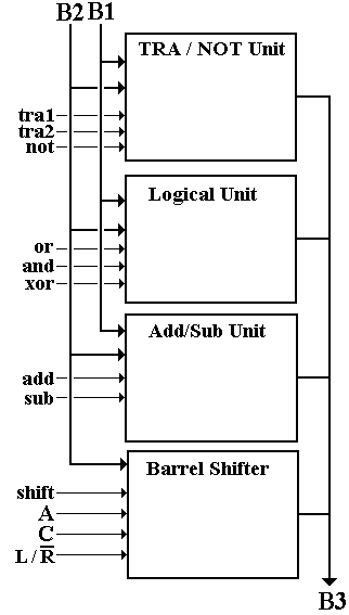 Note that each of buses B1 and B2 feed all of the units
except the barrel shifter, which is fed only by bus B3. All units output on bus B3 and are connected
by tri-state units, so that bus conflicts do not occur. For this first unit, we have
Note that each of buses B1 and B2 feed all of the units
except the barrel shifter, which is fed only by bus B3. All units output on bus B3 and are connected
by tri-state units, so that bus conflicts do not occur. For this first unit, we have
tra1 input
from B1
tra2 input
from B2
not input
from B1
The Logical Unit contains those
Boolean functions that take two inputs.
These are AND, OR, and XOR.
Although the NOT is also a Boolean function, it is more easily placed in
the first unit.
The Adder/Subtractor unit is also a
binary unit and might be placed with the Logical Unit, except that such a
design would appear more complicated than necessary. We design this unit as a standalone module.
The Barrel Shifter accepts input
only from bus B2. We have seen its
design earlier, with the input labeled X31-0 and the output labeled
Y31-0.
Figure: Top-Level ALU Design.
The above control signals are
generally required to be mutually exclusive in order for the ALU to function
correctly. Of the set {tra1, tra2, not,
or, and, xor, add, sub, shift} at most one may be active during any clock pulse
or the ALU will malfunction. The three
shift mode selectors (A, C, and ![]() ) may be asserted in any combination (though A = 1 and
C = 1 is arbitrarily changed to A = 0 and C = 1) and have effect only when shift = 1.
) may be asserted in any combination (though A = 1 and
C = 1 is arbitrarily changed to A = 0 and C = 1) and have effect only when shift = 1.
The TRA / NOT Unit
The design of this unit is particularly
simple. We present the design for a
single bit and note that the complete design just replicates this 32
times. In this and other figures B1K
refers to bit K on bus B1, B2K to bit K on bus B2, and B3K
to bit K on bus B3, with 0 £
K £ 31.
Note the extensive use of tri-state buffers to connect output to bus B3.
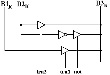
Figure: The TRA/NOT Unit
The
Binary Logical Unit
The design of this unit is also
particularly simple. Again, we show the
design for just one bit and note that the complete design replicates this 32
times.
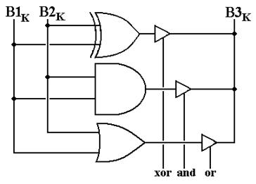
Figure: The Binary Logical Unit
The
Add/Subtract Unit
To avoid additional complexity, we
implement this unit as a 32-bit ripple-carry unit.
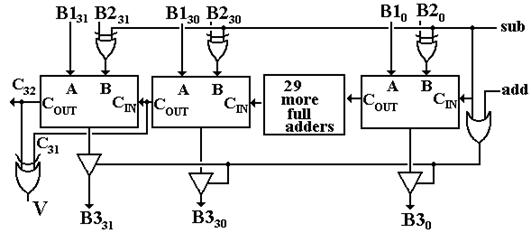
Figure: High and Lower Order Bits of an Adder/Subtractor,
with Overflow Bit V
The
Shifter Unit
All we do here is to attach the
shifter to buses B2 and B3.
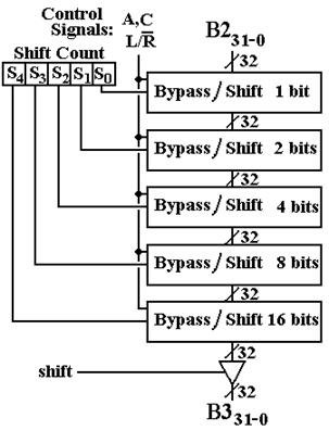
Figure: The Shifter Unit
The
State Registers
We now consider the two state
registers used in the hardwired control unit.
These are the minor state
register (responsible for the four pulses T0, T1, T2, and T3) and the major state register (responsible for
transitions between the three major states: F, D, and A).
The
Minor State Register
The minor state register will be a
modulo–4 counter, implemented as a one-hot design using four D flip-flops. Because of the close association, we shall
also show the RUN flip-flop.
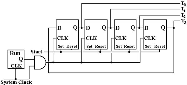
Figure: The
Note that when RUN = 0, the system
clock does not reach the minor state register, which remains frozen in its last
state until the system is restarted. The
Start signal is used to reset the minor state register to T0 =
1. The state register is a four-bit
circular shift register.
This style of shift register is
called “one hot” because, at any given time, only one flip–flop has value 1 and
the rest are set to 0. A design with two
flip–flops and a 2–to–4 decoder could perform an equivalent function, though
with time delays for the state decoding.
The
Major State Register
The function of the major state
register is to control the execution state of the machine language
instructions. The current design has 3
major states: Fetch, Defer, and Execute.
The design of this register is simplified by the fact that almost all of
the instructions execute in the Fetch cycle.
Only eight instructions (GET, PUT, RET, RTI, LDR, STR, BR, and JSR) even
enter the Execute state, much less the Defer state. Recall that GET, PUT, RET, and RTI cannot
enter the Defer stage and that the others enter it only if IR26 = 1.
In the next table, we examine these
instructions closely to determine patterns that will be of use in defining the
Major State Register. For all other
instructions, the state after Fetch is Fetch again; the instruction completes
execution in one major cycle and the next is fetched.
|
|
IR31 |
IR30 |
IR29 |
IR28 |
IR27 |
IR26 = 0 |
IR26 = 1 |
|
GET |
0 |
1 |
0 |
0 |
0 |
Execute |
|
|
PUT |
0 |
1 |
0 |
0 |
1 |
Execute |
|
|
RET |
0 |
1 |
0 |
1 |
0 |
Execute |
|
|
RTI |
0 |
1 |
0 |
1 |
1 |
Execute |
|
|
LDR |
0 |
1 |
1 |
0 |
0 |
Execute |
Defer |
|
STR |
0 |
1 |
1 |
0 |
1 |
Execute |
Defer |
|
JSR |
0 |
1 |
1 |
1 |
0 |
Execute |
Defer |
|
BR |
0 |
1 |
1 |
1 |
1 |
Execute if Branch = 1, Fetch Otherwise |
Defer if Branch = 1, Fetch Otherwise |
We
define two generated control signals, S1 and S2, as
follows:
1. If
the present state is Fetch and S1 = = 0, the next state will be
Fetch.
If the present state is Fetch
and S1 = = 1, the next state is either Defer or Execute.
2. If
the present state is Fetch, S1 = = 1, and S2 = = 0, the
next state will be Execute.
If the present state is Fetch,
S1 = = 1, and S2 = = 1, the next state will be Defer.
3. Automatic
rule: If the present state is Defer, the next state will be Execute.
4. Automatic
rule: If the present state is Execute, the next state will be Fetch.
This leads to the following state diagram for the Major
State Register.
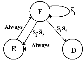
Figure: State Diagram for the Major State Register
A three–state diagram requires two
flip–flops for its implementation. To
begin this design, we assign two–bit binary numbers, denoted Y1Y0,
to each of the major states.
|
State |
Y1 |
Y0 |
|
F |
0 |
0 |
|
D |
0 |
1 |
|
E |
1 |
0 |
The easiest way to implement this
design uses two D flip–flops, with inputs D1 and D0. We are now left with only two questions:
1. How
to generate the two inputs D1 and D0 from S1,
S2, Y0, and Y1.
2. How
to generate S1 and S2 from the op–codes.
It
will be seen below that the circuitry to generate these signals is quite
simple. We first ask ourselves how it
came to be so simple when it had the possibility of great complexity. To see what has happened, we examine the
evolution of the op–codes for the first 12 instructions.
|
Op-Code |
|
Version 1 |
|
Version 2 |
|
Version 3 |
|
Version 4 |
|
00 000 |
|
HLT |
|
HLT |
|
HLT |
|
HLT |
|
00 001 |
|
LDI |
|
LDI |
|
LDI |
|
LDI |
|
00 010 |
|
ANDI |
|
ANDI |
|
ANDI |
|
ANDI |
|
00 011 |
|
ADDI |
|
ADDI |
|
ADDI |
|
ADDI |
|
00 100 |
|
GET |
|
|
|
|
|
|
|
00 101 |
|
PUT |
|
|
|
|
|
|
|
00 110 |
|
LDR |
|
|
|
|
|
|
|
00 111 |
|
STR |
|
|
|
|
|
|
|
01 000 |
|
BR |
|
GET |
|
GET |
|
GET |
|
01 001 |
|
JSR |
|
PUT |
|
PUT |
|
PUT |
|
01 010 |
|
RET |
|
LDR |
|
RET |
|
RET |
|
01 011 |
|
RTI |
|
STR |
|
RTI |
|
RTI |
|
01 100 |
|
|
|
BR |
|
LDR |
|
LDR |
|
01 101 |
|
|
|
JSR |
|
STR |
|
STR |
|
01 110 |
|
|
|
RET |
|
BR |
|
JSR |
|
01 111 |
|
|
|
RTI |
|
JSR |
|
BR |
In
each of these designs, the four “immediate instructions” are allocated the
first 4 op–codes, numbered 0 through 3.
The original idea was that all such instructions would have op–codes
beginning with “000”. This was a good
idea, but has yet to be exploited in these designs.
Version 1
of the list of instructions just presented the instructions in the way the
author thought them up. The instructions
were considered to exist in four groups: GET & PUT; LDR & STR; JSR,
RET, & RTI; and
Version 2
of this list resulted from the observation that introducing four NOP
instructions and moving the instructions beginning with GET down by four would
yield the result that all instructions that could leave the Fetch state would
have op–codes beginning with “01”. This
decision was taken because it introduced a regularity into the pattern of
op–codes and this author expected such a pattern to yield a simplification in
the circuitry.
Version 3
of the list resulted from the observation that moving the RET and RTI
instructions to follow GET and PUT would yield the result that those
instructions that might use the Defer state all began with “011”.
Version 4
of the list is a minor modification of version 3. It is a result of the observation that the
branch instruction, BR, is the only one that has an additional constraint on
its leaving the Fetch state. It leaves
Fetch if and only if the signal Branch = = 1.
This is a time saving feature that avoids computation of an effective
address when the branch is not going to be taken. For this reason, the BR instruction was moved
to last in the list.
We
now repeat the table that began this discussion and recall the definition of
the two generated control signals S1 and S2.
|
|
IR31 |
IR30 |
IR29 |
IR28 |
IR27 |
IR26 = 0 |
IR26 = 1 |
|
GET |
0 |
1 |
0 |
0 |
0 |
Execute |
|
|
PUT |
0 |
1 |
0 |
0 |
1 |
Execute |
|
|
RET |
0 |
1 |
0 |
1 |
0 |
Execute |
|
|
RTI |
0 |
1 |
0 |
1 |
1 |
Execute |
|
|
LDR |
0 |
1 |
1 |
0 |
0 |
Execute |
Defer |
|
STR |
0 |
1 |
1 |
0 |
1 |
Execute |
Defer |
|
JSR |
0 |
1 |
1 |
1 |
0 |
Execute |
Defer |
|
BR |
0 |
1 |
1 |
1 |
1 |
Execute if Branch = 1, Fetch Otherwise |
Defer if Branch = 1, Fetch Otherwise |
We define two generated control signals, S1 and S2,
as follows:
1. If
the present state is Fetch and S1 = = 0, the next state will be
Fetch.
If the present state is Fetch
and S1 = = 1, the next state is either Defer or Execute.
2. If
the present state is Fetch, S1 = = 1, and S2 = = 0, the
next state will be Execute.
If the present state is Fetch,
S1 = = 1, and S2 = = 1, the next state will be Defer.
We
now see the end result of modification of the op–codes:
1. Only
instructions with op–codes beginning with “01” can leave Fetch
2. Only
instructions with op–codes beginning with “011” can enter Defer.
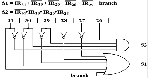
We now derive the equations for the generated control signals.
S1: We note that S1 is 0 when IR31IR30
¹ “01”.
We also note that S1 is 0
when IR31IR30 = “01”, if Branch = 0 and IR29IR28IR27
= “111”.
We could say S1 is 1 when
IR31IR30 = “01”, and either Branch = 1 or IR29-27
¹ “111”.
But IR29-27 ¹ “111” is the same as ![]() . Given this
observation, we see
. Given this
observation, we see
S1 = ![]() ·( Branch +
·( Branch + ![]() ).
).
S2: Given that this signal is used only when S1
is 1, we can proceed from two observations.
1. Only
instructions with IR29 = 1 can enter the defer state.
2. The
defer state is entered by these four instructions only when IR26 =
1.
S2
= IR29 ·
IR26
As an aside, we note that many
textbooks set S2 = IR26,
thus saying that all instructions for which the Indirect bit is set will enter
the defer state. Our definition of S2
= IR29 ·
IR26 and our insistence that Defer is entered only when S1·S2 = 1 avoids traps on bad bits.
Design
of the Major State Register
We now have all we need to complete
a design of the major state register.
1. The register will be designed using two D
flip–flops, with inputs D1 and D0, and
outputs Y1 and Y0. The binary encoding for these states is shown
in the table.
|
State |
Y1 |
Y0 |
|
F |
0 |
0 |
|
D |
0 |
1 |
|
E |
1 |
0 |
2. There
will be two control signals, S1 and S2, to sequence the
register.
If the present state is Fetch
and S1 = = 0, the next state will be Fetch.
If the present state is Fetch,
S1 = = 1, and S2 = = 0, the next state will be Execute.
If the present state is Fetch,
S1 = = 1, and S2 = = 1, the next state will be Defer.
Automatic rule: If the present state
is Defer, the next state will be Execute.
Automatic rule: If the present
state is Execute, the next state will be Fetch.
3. S1
= ![]() ·( Branch +
·( Branch + ![]() ).
).
S2 = IR29
· IR26
4. We note that the circuit, when operating
properly, never has both D1 = 1 and D0 = 1.
Thus we may say that D1 = conditions to move to Execute
D0
= conditions to move to Defer
So
we have the following equations:
D0 = F·S1·S2
D1 = ![]() + D // D = 1 if and only if in the
Defer state
+ D // D = 1 if and only if in the
Defer state
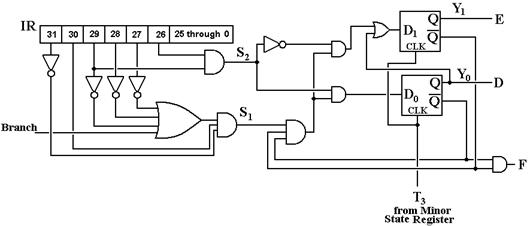
Figure: The Major State Register of the
Boz–7
Note that the trigger for the
transition between major states is T3 from the minor state
register. When it is active, the minor
state register continuously cycles through its states, and the major state
register changes to its next state when triggered.
Instruction
Decoder
The function of the Instruction
Decoder is to take the output of the appropriate bits of the IR (Instruction
Register) and generate the discrete signal associated with the
instruction. Note that the discrete
signal associated with an assembly language instruction has the same name; thus
LDI is the discrete signal asserted when the op-code in the IR is 000001, which
is associated with the LDI (Load Register Immediate) assembly language
instruction.
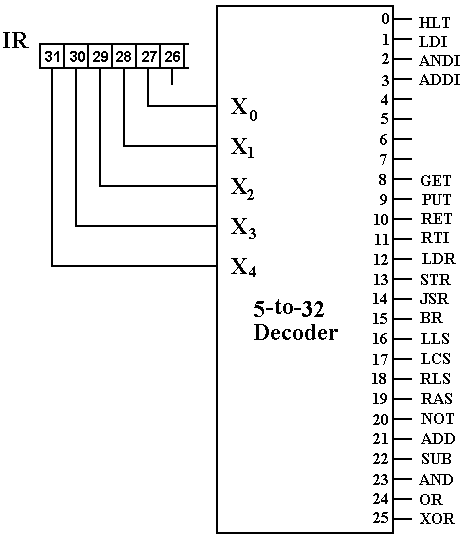
Figure: The Decoding of IR31-27 into Discrete
Signals for the Instructions
The instruction decoder is
implemented as a simple 5–to–32 decoder, in that there are five bits in the
op–code and a maximum of 32 instructions.
To save space outputs 26 – 31 of the decoder are not shown. Also, outputs 4 – 7 of the decoder are not
connected to any circuit, indicating that these op–codes are presently NOP’s.
Signal
Generation Tree
We now have the three major parts of
circuits required to generate the control signals.
1) the
major state register (F, D, and E),
2) the
minor state register (T0, T1, T2, and T3), and
3) the
instruction decoder.
Common
Fetch Cycle
In hardwired control units, these
and some other condition signals are used as input to combinational circuits
for generation of control signals. As an
example, we consider the generation of the control signals for the first three
steps of the fetch phase. Note that
these signals are common for all machine language instructions, as (F, T2)
results in the placing of the instruction into the Instruction Register, from
whence it is decoded.
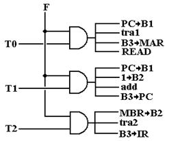
Figure: Control Signals for the Common Fetch Sequence
This figure involves logical signal, asserted to either 0 or
1. Each output of the AND gates should
be viewed also as a discrete logic signal, which when asserted as 1 causes an action
(indicated by the signal name) to take place.
Thus, when F = 1 and T2 = 1 (indicating that the control unit is in step
T2 of the Fetch state), then the three signals MBR ® B2, tra2, and B3
® IR are asserted as logic 1. The assertion of the signal MBR ® B2 as logic 1 causes the contents of the MBR register to be
transferred to bus B2. The assertion of
signal tra2 to logic 1 causes the
contents of bus B2 to be transferred through the ALU and onto bus B3. The assertion of signal B3 ® IR to logic 1 causes the contents of bus B3 to be copied
into the Instruction Register, also called the IR.
There is one obvious remark about
the above drawing. Notice that each of
the top two AND gates generates a signal labeled “PC ® B1”. At some point
in the design, these and any other identical signals are all input into an OR
gate used to effect the actual transfer.
The reader will note that we now
have terminology that must be used carefully.
Consider the machine language instruction with op-code = 10101. There are 3 terms associated with this.
ADD the mnemonic for the assembly language instruction associated, and
ADD the discrete signal (logic 0 or logic 1) emitted by the
instruction decoder, and
add the discrete signal
emitted by the control unit that causes the ALU to add.
The first and second used of the term “ADD” are distinguished by context.
Whenever the term is used as a logic signal, it cannot be the assembly language
mnemonic.
Defer
Cycle
We now show the only other part of
the signal generation tree that is independent of the machine language
instruction being executed. This is the
tree for signals associated with the Defer phase of execution. The reader will recall that only three
instructions (LDR, STR, and BR) can enter the Defer phase, and then only when
IR26 = 1. Note that there are
no signals generated for T1 or T3 during the Defer phase, because nothing
happens at those times.
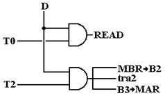
Figure: Control Signals for the Defer
The
Rest of Fetch
We now investigate the control
signals issued during step T3 of Fetch for the rest of the instructions. We use the next table to investigate
commonalities in the signal generation.
|
Op–Code |
|
B1 |
B2 |
B3 |
ALU |
Other |
||||
|
IR31 |
IR30 |
IR29 |
IR28 |
IR27 |
|
|
|
|
|
|
|
0 |
0 |
0 |
0 |
0 |
HLT |
|
|
|
|
0 ®
RUN |
|
0 |
0 |
0 |
0 |
1 |
LDI |
IR |
|
R |
tra1 |
|
|
0 |
0 |
0 |
1 |
0 |
ANDI |
IR |
R |
R |
and |
|
|
0 |
0 |
0 |
1 |
1 |
ADDI |
IR |
R |
R |
add |
|
|
0 |
1 |
0 |
0 |
0 |
GET |
|
|
|
|
|
|
0 |
1 |
0 |
0 |
1 |
PUT |
|
|
|
|
|
|
0 |
1 |
0 |
1 |
0 |
RET |
|
|
|
|
|
|
0 |
1 |
0 |
1 |
1 |
RTI |
|
|
|
|
|
|
0 |
1 |
1 |
0 |
0 |
LDR |
IR |
R |
MAR |
add |
|
|
0 |
1 |
1 |
0 |
1 |
STR |
IR |
R |
MAR |
add |
|
|
0 |
1 |
1 |
1 |
0 |
JSR |
IR |
R |
MAR |
add |
|
|
0 |
1 |
1 |
1 |
1 |
BR |
IR |
R |
MAR |
add |
|
|
1 |
0 |
0 |
0 |
0 |
LLS |
|
R |
R |
shift |
1, 0, 0* |
|
1 |
0 |
0 |
0 |
1 |
LCS |
|
R |
R |
shift |
1, 0, 1 |
|
1 |
0 |
0 |
1 |
0 |
RLS |
|
R |
R |
shift |
0, 0, 0 |
|
1 |
0 |
0 |
1 |
1 |
RAS |
|
R |
R |
shift |
0, 1, 0 |
|
1 |
0 |
1 |
0 |
0 |
NOT |
|
R |
R |
not |
|
|
1 |
0 |
1 |
0 |
1 |
ADD |
R |
R |
R |
add |
|
|
1 |
0 |
1 |
1 |
0 |
SUB |
R |
R |
R |
sub |
|
|
1 |
0 |
1 |
1 |
1 |
AND |
R |
R |
R |
and |
|
|
1 |
1 |
0 |
0 |
0 |
OR |
R |
R |
R |
or |
|
|
1 |
1 |
0 |
0 |
1 |
XOR |
R |
R |
R |
xor |
|
*Shift control signals: L/R’, A, and
C; for Left/Right, Arithmetic, and Circular
While we certainly could focus on
generation of a set of signals for each of the twenty–two instructions in the
above table, we shall use the commonalities displayed by the table to simplify
the signal tree considerably. We begin
with a consideration of the first four instructions, as these contain an
insight that will yield significant reductions in complexity.
|
Op–Code |
|
B1 |
B2 |
B3 |
ALU |
Other |
||||
|
IR31 |
IR30 |
IR29 |
IR28 |
IR27 |
|
|
|
|
|
|
|
0 |
0 |
0 |
0 |
0 |
HLT |
|
|
|
|
0 ®
RUN |
|
0 |
0 |
0 |
0 |
1 |
LDI |
IR |
|
R |
tra1 |
|
|
0 |
0 |
0 |
1 |
0 |
ANDI |
IR |
R |
R |
and |
|
|
0 |
0 |
0 |
1 |
1 |
ADDI |
IR |
R |
R |
add |
|
The bus allocations for these instructions are obvious, but
worth note. The LDI instruction has no
allocation for bus B2. Suppose we
allocated a general–purpose register to B2.
Then some random register would have its contents transferred to bus B2,
only to be ignored by the ALU which is executing a tra1 instruction. Now consider the HLT instruction. Here we might also allocate registers to both
bus B1 and bus B2, as the ALU is not active and does nothing with its
input. Hence the table above might as
well be the following.
|
Op–Code |
|
B1 |
B2 |
B3 |
ALU |
Other |
||||
|
IR31 |
IR30 |
IR29 |
IR28 |
IR27 |
|
|
|
|
|
|
|
0 |
0 |
0 |
0 |
0 |
HLT |
IR |
R |
|
|
0 ®
RUN |
|
0 |
0 |
0 |
0 |
1 |
LDI |
IR |
R |
R |
tra1 |
|
|
0 |
0 |
0 |
1 |
0 |
ANDI |
IR |
R |
R |
and |
|
|
0 |
0 |
0 |
1 |
1 |
ADDI |
IR |
R |
R |
add |
|
One might legitimately ask why not go “whole hog” and
allocate a register to B3 for the HLT instruction. The answer is that such an action would cause
some random register to become corrupted as it would cause data (possibly all
0’s) to be input to the selected register.
It is very likely that register %R0 would be selected, resulting in a
NOP, but the designer of a control unit cannot make such assumptions.
Examining the above table, we come to the following
conclusions.
1) We
use the ALU code to differentiate between the instructions, placing registers
on
buses B1 and B2 in any way
that does not cause problems.
2) The rule for bus B1 is as follows: IR ® B1 if IR31 = = 0 and R ® B1 if IR31 = = 1.
This will cause IR ® B1 for the GET, PUT, RET, and RTI instructions, but that is
not a problem as the ALU does
nothing for these. It will cause R ® B1 for the shift
and NOT instructions, but that also is not
problem as only bus B2 is input to these.
3) The rule for bus B2 is as follows: R ® B2 always. The only
instructions that do not
call for such are HLT, LDI,
GET, PUT, RET, and RTI. The last four do
nothing in
this minor cycle, and the
first two are not made to be incorrect by the assignment.
4) The handling of bus B3 is trickier. If IR31-29 = = “011”, we have B3 ® MAR. If
either IR31 = = 1
or IR31-27 = = “00001”, “00010”, or “00011”, then B3 ® R. A bit
of Boolean algebra yields the
condition for B3 ®
R as follows:
( IR31 = = 1 ) OR [
( IR30 = = 0 ) AND ( IR29 = = 0 ) AND ( IR28 +
IR27 = = 1 ) ]
Here is the complete signal
generation tree for the T3 minor cycle in the Fetch major cycle. Note that the signals output from the AND
gates to the right of the tree are control signals that activate actual
transfers; thus “IR ®
B1” causes the contents of the IR (Instruction Register) to be transferred to
bus B1.
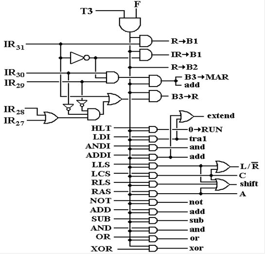
Figure: Signal Generation Tree for
Fetch, T3
Note that the last fourteen entries
on the left side of the signal tree are all in upper case letters. Each of these is the control signal generated
by the instruction decoder based on the op–code bits in the Instruction
Register. The entries in lower case, to
the right of the signal tree, are control signals to the ALU.
Study
of the Execute Phase
The reader will recall that only eight instructions access this state. These instructions are
GET, PUT, RET, RTI (Not Implemented), LDR, STR, JSR, and
At this point, we make two remarks
that are only marginally related to this study.
1. The original design for the control signal
had both the STR (store register) and
BR (branch) issue their final
control signal in (E, T2). This lead to
the following
counts for control signals in
Execute: 5, 2, 6, and 2. The final
signal for STR
could not be later than (E,
T2) so it was moved to (E, T1). The
final signal for BR
could occur any time in the
Execute phase, so it was moved to (E, T3).
This resulted
in the counts: 5, 3, 4, and 3.
2. The name “Execute” for this phase is a bit
awkward. The Fetch phase is so named
because if fetches the
instruction. The Defer phase is so named
because it calculates
the deferred address. The Execute phase does contain execution
logic for eight of
the instructions, but the
majority of the instructions complete execution in the Fetch
phase. There is simply no good name for this phase.
Execute, T0
GET: IR ® B1, tra1, B3 ® IOA. //
Send out the I/O address
PUT: R
® B2, tra2, B3 ®
IOD // Get the
data ready
RET: SP
® B1, + 1 ® B2, add, B3 ® SP. //
Increment the SP
LDR: READ. //
Address is already in the MAR.
JSR: PC
® B1, tra1, B3 ®
MBR. // Put return
address in MBR
Execute, T1
RET: SP ® B1, tra1, B3 ® MAR, READ. //
Get the return address
STR: R
® B1, tra1, B3 ® MBR, WRITE.
JSR: MAR
® B1, tra1, B3 ®
PC. //
Set up for jump to target.
Execute, T2
GET: IOD ® B2, tra2, B3 ® R. //
Get the results.
PUT: IR
® B1, tra1, B3 ®
IOA. // Sending
out the address
LDR: MBR
® B2, tra2, B3 ® R.
JSR: SP ®
B1, tra1, B3 ® MAR, WRITE. //
Put return address on stack.
Execute, T3
RET: MBR
® B2, tra2, B3 ®
PC. // Put return
address into P
JSR: SP
® B1, 1 ® B2, sub, B3 ® SP. // Decrement
the SP
BR: MAR
® B1, tra1, B3 ® PC.
The
We now show the signal generation trees for the
Figure: Control Signals for the Execute State
The reader should remember that the
Major State Register will enter the
Micro–Programmed
Version of the Control Unit
We have just shown the signal
generation trees for the hardwired version of the control unit. We now present the micro–programmed version
of the same unit.
We begin with a summary of the
control signals used. This table is just
a listing of the signals. At some time
later, these signals will be assigned numeric codes and the table shown in
another presentation. Note that the
first row in the table is unlabeled, reflecting the fact that we must allow for
no activity on each of the units.
|
Bus 1 |
Bus 2 |
Bus 3 |
ALU |
Other |
|
|
|
|
|
|
|
PC ®
B1 |
1 ®
B2 |
B3 ®PC |
tra1 |
L / R’ |
|
MAR ®
B1 |
|
B3 ®
MAR |
tra2 |
A |
|
R ®
B1 |
R ®
B2 |
B3 ®
R |
shift |
C |
|
IR ®
B1 |
MBR ®
B2 |
B3 ®
IR |
not |
READ |
|
SP ®
B1 |
IOD ®
B2 |
B3 ®
SP |
add |
WRITE |
|
|
|
B3 ®
MBR |
sub |
extend |
|
|
|
B3 ®
IOD |
and |
0 ®
RUN |
|
|
|
B3 ®
IOA |
or |
|
|
|
|
|
xor |
|
Microcoding (microprogramming) is another way of generating
control signals. Rather than generating
these signals from hardwired gates, these are generated from words in a memory
unit, called a micro–memory. To
illustrate this concept, consider a simple micro–controller to generate control
signals for bus B1.
Figure: A Sample Micro–Memory
Here we see an example, written in
the style of horizontal micro–coding (soon to be defined) with one bit in the
micro–memory for each of the control signals to be emitted. When the word at micro–address 105 is read
into the micro–MBR (the register at the bottom), the control signals generated
are PC ® B1 = 0, MAR ® B1 = 1, R ®
B1 = 0, IR ® B1 = 0, and SP ® B1 = 0. Thus,
copying micro–word 105 into the Micro–MBR asserts
MAR ® B1.
Similarly, copying micro–word 106 into the Micro–MBR asserts R ® B1.
Horizontal
vs. Vertical Micro–Code
The micro–programming strategy called “horizontal
microcode” allows one bit in the micro–memory for each control signal
generated. We have illustrated this with
a small memory to issue control signals for bus B1. There are five control signals associated
with this bus, so this part of the micro–memory would comprise five–bit
numbers.
A quick count from the table of
control signals shows that there are thirty–four discrete control signals
associated with this control unit. A
full horizontal implementation of the microcode would thus require 34 bits in
each micro–word just to issue the control signals. The memory width is not a big issue; indeed
there are commercial computers with much wider micro–memories. We just note the width requirement.
In vertical microcoding, each signal is assigned a numeric code that
is unique for its function. Thus, each
of the five signals for control of bus B1 would be assigned a numeric
code. The following table illustrates
the codes actually used in the design of the Boz–7.
|
Code |
Signal |
|
000 |
|
|
001 |
PC ®
B1 |
|
010 |
MAR ®
B1 |
|
011 |
R ®
B1 |
|
100 |
IR ®
B1 |
|
101 |
SP ®
B1 |
It is particularly important that a vertical microcoding
scheme allow for the option that no signal is being placed on the bus. In this design we reserve the code 0 for
“nothing on bus” or “ALU does nothing”, etc.
The three bits in this design are placed into a 3–to–8 decoder, as shown
in the figure below. Admittedly, this
design is slower than the horizontal microcode in that it incurs the time
penalty associated with the decoder.
Figure: Sample of Vertical Microcoding
In this revised example, word 105
generates MAR ®
B1 and word 106 generates R ®
B1.
One advantage of encoding the
control signals is the unique definition of the signal for each function. As an example, consider both the horizontal and
vertical encodings for bus B1. In the
five–bit horizontal encoding, we were required to have at most one 1 per
micro–word. An examination of that
figure will show that the micro–word “10100” would assert the two control
signals PC ® B1 and R ® B1 simultaneously, causing considerable difficulties. In the vertical microcoding example, the
three–bit micro–word with contents “011” causes the control signal R ® B1, and only that control signal, to be asserted. To be repetitive, the code “000” is reserved for
not specifying any source for bus B1; in which case the contents of the bus are
not specified. In such a case, the ALU
cannot accept input from bus B1.
The design chosen for the microcode
will be based on the fact that four of the CPU units
(bus B1, bus B2, bus B3, and the ALU) can each have only one “function”. For this reason, the control signals for
these units will be encoded. There are
seven additional control signals that could be asserted in any
combination. These signals will be
represented in horizontal microcode, with one bit for each signal.
Structure
of the Boz–7 Microcode
As indicated above, the Boz–7 microcode will be a mix of horizontal and
vertical microcode. The reader will note
that some of the encoded fields require 3–bit codes and some require 4–bit
codes. For uniformity of notation we
shall require that each field be encoded in 4 bits. The requirement that each field be encoded by
a 4–bit binary number has no justification in engineering practice. Rather it is a convenience to the student,
designed to remove at least one minor nuisance from the tedium of writing
binary microcode and converting it to hexadecimal format. Four binary bits correspond to one hex digit.
Consider the following example,
taken from the common fetch sequence.
MBR
® B2, tra2, B3 ® IR.
A minimal–width encoding of this
sequence of control signals would yield the following.
0
000 110 100 010 000 0000 0000 0000 0000 0000.
Conversion of this to hexadecimal
requires regrouping the bits and then rewriting.
0000
1101 0001 0000 0000 0000 0000 0000 0000 or 0x0 D100 0000
The four–bit constant width coding
of this sequence yields the following.
0000
0000 0110 0100 0010 0000 0000 0000 0000 0000 0000
This is immediately converted to
0x006 4200 0000 without shuffling any bits.
Dispatching
the Microcode
In addition to micro–words that
cause control signals to be emitted, we need micro–words to sequence the
execution of the microcode. This is seen
most obviously in the requirement for a dispatch based on the assembly language
op–code. Let’s begin with an observation
that is immediately obvious. If the
microprogrammed control unit is to handle each distinct assembly language opcode
differently, it must have sections of microprogram that are unique to each of
the assembly language instructions.
The solution to this will be a dispatch microoperation, one which
invokes a section of the microprogram that is selected based on the 5–bit
opcode that is currently in the Instruction Register. But what is called and how does it return?
The description above suggests the
use of a micro–subroutine, which would be the microprogramming equivalent of a
subroutine in either assembly language or a higher level language. This option imposes a significant control
overhead in the microprogrammed control unit, one that we elect not to take.
The “where to return issue” is
easily handled by noting that the action next after executing any assembly
language instruction is the fetching of the next one to execute. For reasons that will soon be explained, we
place the first microoperation of the common fetch sequence at address 0x20 in
the micromemory; each execution phase ends with “go to 0x20”.
The structure of the dispatch
operation is best considered by examination of the control signals for the
common fetch sequence.
F,
T0: PC ® B1, tra1, B3 ® MAR, READ. //
MAR ¬ (PC)
F, T1: PC ®
B1, 1 ® B2, add, B3 ® PC. // PC
¬ (PC) + 1
F, T2: MBR ®
B2, tra2, B3 ®
IR. // IR ¬ (MBR)
F, T3: Do something specific to the opcode in the IR.
In the hardwired control unit, the
major and minor state registers would play a large part in generation of the
control signals for (F, T3) and the major state register would handle the
operation corresponding to “dispatch”, that is selection of what to do next. Proper handling of the dispatch in the
microprogrammed control unit requires an explicit micro–opcode and a slight
resequencing of the common fetch control signals. Here is the revised sequence.
F,
T0: PC ® B1, tra1, B3 ® MAR, READ. //
MAR ¬ (PC)
F, T1: PC ®
B1, 1 ® B2, add, B3 ® PC. // PC
¬ (PC) + 1
F, T2: MBR ®
B2, tra2, B3 ®
IR. // IR ¬ (MBR)
Dispatch
based on the assembly language opcode
F,
T3: Do something specific to the
opcode in the IR.
The next issue for our consideration
in the design of the structure of the microprogram is a decision on how to
select the address of the micro–instruction to be executed next after the
current micro–instruction. In order to
clarify the choices, let’s examine the microprogram sequence for a specific
assembly language instruction and see what we conclude.
The assembly language instructions
that most clearly illustrate the issue at hand are the register–to–register
instructions. We choose the logical AND
instruction and arbitrarily assume that its microprogram segment begins at
address 0x80 (a new design, to be developed soon, will change this) and see
what we have. Were we to base our
control sequence on the model of assembly language programming, we would write
it as follows.
0x20 PC ® B1, tra1, B3 ® MAR, READ. //
MAR ¬ (PC)
0x21 PC
® B1, 1 ® B2, add, B3 ® PC. // PC
¬ (PC) + 1
0x22 MBR
® B2, tra2, B3 ® IR. //
IR ¬ (MBR)
0x23 Dispatch
based on the assembly language opcode
0x80 R ® B1, R ®
B2, and, B3 ® R.
0x81 Go
to 0x20.
While the above sequence corresponds
to a coding model that would be perfectly acceptable at the assembly language
level, it presents several significant problems at the microcode level. We begin with the observation that it requires
the introduction of an explicitly managed microprogram counter in addition to
the micro–memory address register.
The second, and most significant,
drawback to the above design is that it requires two clock pulses to execute
what the hardwired control unit executed in one clock pulse. One might also note that the present design
calls for using two micro–words (addresses 0x80 and 0x81) where one micro–word
might do. This is a valid observation,
but the cost of memory is far less significant than the “time cost” to execute
the extra instruction.
The design choice taken here is to
encode the address of the next microinstruction in each microinstruction in the
microprogram. This removes the
complexity of managing a program counter and the necessity of the time–consuming
explicit branch instruction. Recasting
the example above in the context of our latest decision leads to the following
sequence.
Address Control Signals Next address
0x20 PC ® B1, tra1, B3 ® MAR, READ. 0x21
0x21 PC ®
B1, 1 ® B2, add, B3 ® PC. 0x22
0x22 MBR ®
B2, tra2, B3 ®
IR. 0x23
0x23 Dispatch based on IR31–IR27. ?? – We decide later
0x80 R ® B1, R ®
B2, and, B3 ® R. 0x20
Note that the introduction of an
explicit next address causes the execution phase of the logical AND instruction
to be reduced to one clock pulse, as desired.
The requirement for uniformity of microcode words leads to use of an
explicit next address in every micro–word in the micromemory. The only microinstruction that appears not to
require an explicit next address in the dispatch found at address 0x23.
A possible use for the next address
field of the dispatch instruction is seen when we consider the effort put into
the hardwired control unit to avoid wasting execution time on a Branch
instruction when the branch condition was not met. The implementation of this decision in a
microprogrammed control unit is to elect not to dispatch to the opcode–specific
microcode when the instruction is a branch and the condition is not met. What we have is shown below.
Address Control Signals Next address
0x20 PC ® B1, tra1, B3 ® MAR, READ. 0x21
0x21 PC ®
B1, 1 ® B2, add, B3 ® PC. 0x22
0x22 MBR ®
B2, tra2, B3 ®
IR. 0x23
0x23 Dispatch based on IR31–IR27. 0x20
0x80 R ® B1, R ®
B2, and, B3 ® R. 0x20
The present design places the next
address for dispatch when the condition is not met in the field of the
micro–word associated with the next address for two reasons:
1. This results in a more regular design, one
that is faster and easier to implement.
2. This avoids “hard coding” the address of the
beginning of the common fetch.
At this point in the design of the
microprogrammed control unit, we have two distinct types of microoperations: a
type that issues control signals and a type that dispatches based on the
assembly language opcode. To handle this
distinction, we introduce the idea of a micro–opcode
with the following values at present.
Micro–Op Function
0000 Issue control signals
0001 Dispatch based on the
assembly language opcode.
We have stated that there are
conditions under which the dispatch will not be taken. There is only one condition that will not be
dispatched: the assembly–language opcode is 0x0F and the branch condition is
not met. Before we consider how to
handle this situation, we must first address another design issue, that
presented by indirect addressing.
Handling Defer
Consider the control signals for the
LDR (Load Register) assembly language instruction.
LDR Op-Code = 01100 (Hexadecimal
0x0C)
F,
T0: PC ® B1, tra1, B3 ® MAR, READ. //
MAR ¬ (PC)
F, T1: PC ®
B1, 1 ® B2, add, B3 ® PC. // PC
¬ (PC) + 1
F, T2: MBR ®
B2, tra2, B3 ®
IR. // IR ¬ (MBR)
F, T3: IR ®
B1, R ® B2, add, B3 ®
MAR. // Do the indexing.
Here the major state register takes control.
1) If the I–bit (bit 26) is 1, then the Defer
state is entered.
2) If
the I–bit is 0, then the E state is
entered.
D,
T0: READ. //
Address is already in the MAR.
D, T1: WAIT. //
Cannot access the MBR just now.
D, T2: MBR ®
B2, tra2, B3 ®
MAR. // MAR ¬ (MBR)
D, T3: WAIT.
Here
the transition is automatic from the D state to the E state.
E,
T0: READ. // Again,
address is already in the MAR.
E, T1: WAIT.
E, T2: MBR ®
B2, tra2, B3 ®
R.
E, T3: WAIT.
The issue here is that we no longer
have an explicit major state register to handle the sequencing of major
states. The microprogram itself must
handle the sequencing; it must do something different for each of the two
possibilities: indirect addressing is used and indirect addressing is not
used. Assuming a dispatch to address
0x0C for LDR (as it will be done in the final design), the current design calls
for the following microinstruction at that address.
Address Control Signals Next
address
0x0C IR ® B1, R ®
B2, add, B3 ® MAR. Depends on
IR26.
Suddenly we need two “next
addresses”, one if the defer phase is to be entered and one to be used if that
phase is not to be entered. This last
observation determines the final form of the microprogram; each micro–word has
length 44 bits with structure as shown below.
In this representation of the
microprogram words, we use “D = 0” to indicate that the defer phase is not to
be entered and “D = 1” to indicate that it should be entered. This notation will be made more precise after
we explore the new set of signals used to control the sequencing of the
microprogram. Here we assume no more
than 256 micro–words in the control store.
|
Micro–Op |
B1 |
B2 |
B3 |
ALU |
M1 |
M2 |
D
= 0 |
D
= 1 |
|
4
bit |
4
bit |
4
bit |
4
bit |
4
bit |
4
bit |
4
bit |
8
bit |
8
bit |
Notes:
1. The
width of each field is either four or eight bits. The main reason for this is
to facilitate the use of
hexadecimal notation in writing the microcode.
2. The use of four bits to encode only two
options for the micro–opcode may appear
extravagant. This follows our desire for a very regular
structure.
3. The use of “D = 0” and “D = 1” is not exactly
appropriate for the dispatch
instruction with micro–opcode
= 0001. We shall explain this later.
4. The bits associated with the M1 field are
those specifying the shift parameters
Bit 3 L / ![]() (1
for a left shift, 0 for a right shift)
(1
for a left shift, 0 for a right shift)
Bit 2 A (1 for
an arithmetic shift)
Bit 1 C (1 for
circular shift)
Bit 0 Not used
5. The bits associated with the M2 field are
Bit 3 READ (Indicates
a memory reference)
Bit 2 WRITE (Unless READ
= 1)
Bit 1 extend (Sign–extend
contents of IR when copying to B1)
Bit 0 0 ®
RUN (Stop the computer)
6. For almost every micro–instruction, the two
“next addresses” are identical. For
these, we cannot predict the
value of the generated control signal “branch” and do
not care, since the next
address will be independent of that value.
7. The values for next addresses will each be
two hexadecimal digits. It is here that
we have made the explicit
assumption on the maximum size of the micromemory.
Sequencing
the Boz–7 Microprogrammed Control Unit
In addition to the assembly language
opcode, we shall need two new signals in order to sequence the microprogrammed
control unit correctly. We call these
two control signals “S1” and “S2”, because they resemble the control signals S1
and S2 used in the hardwired control unit but are not exactly
identical.
In the hardwired control unit, the
signal S1 was used to determine whether or not the state following
Fetch would again be Fetch. This allowed
completion of the execution of 14 of the 22 assembly language instructions in
the Fetch phase. In the microprogrammed
control unit, the signal S1 will be used to determine whether or not the
dispatch microinstruction is executed.
The only condition under which it is not executed is that in which the
assembly language calls for a conditional branch and the branch condition is
not met.
This leads to a simple statement
defining this sequencing signal.
S1
= 0 if and only if the assembly
language opcode = 0x0F and branch =
0,
where branch = 1 if and only if the branch
condition is met.
The sequencing signal S2 is used to
control the entering of the defer code for those instructions that can use
indirect addressing. Recall that the
assignment of opcodes to the assembly language instructions has been structured
so that only instructions beginning with “011” can enter the defer phase. Even these enter the defer phase only when IR26
= 1.
Thus, we have the following definition of this signal.
S2
= 1 if and only if (IR31
= 0, IR30 = 1, IR29 = 1, and IR26 = 1)
In a way, this is exactly the
definition of the sequencing control signal S2 as used in the
hardwired control unit. The only
difference is that in this design the signal S2 must be used independently of
the signal S1, so we must use the full definition. The figure below illustrates the circuitry to
generate the two sequencing signals S1 and S2.
Given these circuits, we have the final form and labeling of
the micro–words in the micro–memory.
Note that there are no “micro–data” words, only microinstructions.
|
Micro–Op |
B1 |
B2 |
B3 |
ALU |
M1 |
M2 |
S2
= 0 |
S2
= 1 |
|
4
bit |
4
bit |
4
bit |
4
bit |
4
bit |
4
bit |
4
bit |
8
bit |
8
bit |
The form of the type 1 instruction is completely defined and
can be given as follows.
|
Micro–Op |
B1 |
B2 |
B3 |
ALU |
M1 |
M2 |
D
= 0 |
D
= 1 |
|
0001 |
0x0 |
0x0 |
0x0 |
0x0 |
0x0 |
0x0 |
0x20 |
0x20 |
But what exactly does this dispatch instruction do? The question becomes one of defining the
dispatch table, which is used to determine the address of the microcode that is
invoked explicitly by this dispatch. We now
address that issue.
The design of the Boz–7 uses a
dispatch mechanism copied from that used by Andrew S. Tanenbaum in his textbook
Structured Computer Organization [R15].
It is apparent that this dispatch mechanism is commonly used in many
commercial implementations of microcode.
The solution is to use the opcode
itself as the dispatch address. As the
Boz–7 uses a five bit opcode, the sequencer unit for the microprogrammed
control unit must expand it to an 8–bit address by adding three high order 0 bits
so that the dispatch address is 000 ¢ IR31–27.
As an example, the binary opcode for LDR is 01100; its dispatch address
is 0000 1100 or 0x0C.
The Boz–7 uses five–bit opcodes,
with range 0x00 through 0x1F. It then
follows that addresses 0x00 through 0x1F in the micromemory must be reserved
for dispatch addresses. It is for this
reason that the common fetch sequence begins at address 0x20; that is the next
available address. We now see that this
structure works only because the address of the next microinstruction is
explicitly encoded in the microinstruction.
This dispatch mechanism works very
well on the 14 of 22 assembly language instructions that complete execution in
one additional clock pulse. As examples,
we examine the control signals for the first 8 opcodes (0x00 – 0x07) along with
the common fetch microcode.
Address Micro Control Signals Next
Address
Opcode S2
= 0 S2 = 1
0x00 0 0
® RUN 0x20 0x20
0x01 0 IR
® B1, extend, tra1, B3 ® R 0x20 0x20
0x02 0 IR
® B1, R ® B2, and, B3 ® R 0x20 0x20
0x03 0 IR
® B1, R ® B2, extend, add, B3 ®R 0x20 0x20
0x04 0 NOP 0x20 0x20
0x05 0 NOP 0x20 0x20
0x06 0 NOP 0x20 0x20
0x07 0 NOP 0x20 0x20
0x20 0 PC
® B1, tra1, B3 ®
MAR, READ 0x21 0x21
0x21 0 PC
® B1, 1 ® B2, add, B3 ® PC 0x22 0x22
0x22 0 MBR
® B2, tra2, B3 ®
IR 0x23 0x23
0x23 1 Dispatch
based on opcode 0x20 0x20
At this point, our design continues to look sound. Note that the unused opcodes (those at
microprogram addresses 0x04 through 0x07) simply do nothing and return to the
common fetch sequence at address 0x20.
This allows for future expansion of the instruction set.
The only problem left to be
addressed is the proper handling of instructions that require more than one
clock cycle (following the common fetch) in which to execute. The first such instruction is the GET
assembly language instruction.
The control signals for the GET
assembly language instruction, as implemented in the hardwired control unit are
shown below. Note that (F, T3) here does
nothing as the instruction cannot be completed in Fetch and I decided not to
make the (F, T3) signal generation tree more complex when I could force the
execution into (E, T0) and (E, T2).
GET Op-Code = 01000 (Hexadecimal
0x08)
F,
T0: PC ® B1, tra1, B3 ® MAR, READ. //
MAR ¬ (PC)
F, T1: PC ®
B1, 1 ® B2, add, B3 ® PC. // PC
¬ (PC) + 1
F, T2: MBR ®
B2, tra2, B3 ®
IR. // IR ¬ (MBR)
F, T3: NOP.
E,
T0: IR ® B1, tra1, B3 ® IOA. //
Send out the I/O address
E, T1: WAIT.
E, T2: IOD ®
B2, tra2, B3 ® R. //
Get the results.
E, T3: NOP.
Noting that the NOP microoperations
in this sequence are used only because there is nothing that can be done during
those clock pulses, we can rewrite the sequence as follows.
GET Op-Code = 01000 (Hexadecimal
0x08)
T0: PC ® B1, tra1, B3 ® MAR, READ. //
MAR ¬ (PC)
T1: PC
® B1, 1 ® B2, add, B3 ® PC. // PC
¬ (PC) + 1
T2: MBR
® B2, tra2, B3 ® IR. //
IR ¬ (MBR)
T3: IR
® B1, tra1, B3 ®
IOA. // Send out
the I/O address
T4: IOD
® B2, tra2, B3 ®
R. // Get the
results.
This fits into the structure of the
microcode fairly well, except that it seems to call for two instructions to be
placed at address 0x08. The solution to
the problem is based on the fact that each microinstruction must encode the
address of the next microinstruction.
Just select the next available word in micromemory and place the “rest
of the execution sequence” there. What
we have is as follows.
Address Micro Control Signals Next
Address
Opcode S2
= 0 S2 = 1
0x08 0 IR
® B1, tra1, B3 ®
IOA. 0x24 0x24
0x20 0 PC
® B1, tra1, B3 ®
MAR, READ 0x21 0x21
0x21 0 PC
® B1, 1 ® B2, add, B3 ® PC 0x22 0x22
0x22 0 MBR
® B2, tra2, B3 ®
IR 0x23 0x23
0x23 1 Dispatch
based on opcode 0x20 0x20
0x24 0 IOD
® B2, tra2, B3 ®
R. 0x20 0x20
In software engineering, such a
structure is called “spaghetti code” and is highly discouraged. The reason is simple; one writes a few
thousand lines in this style and nobody (including the original author) can
follow the logic. The microprogram,
however, comprises a small number (fewer than 33) independent threads of short
(less than 12) instructions. For such a
structure, even spaghetti code can be tolerated.
Assignment
of Numeric Codes to Control Signals
We now start writing the microcode. This
step begins with the assignment of numeric values to the control signals that
the control unit emits.
The next table shows the numeric
codes that this author has elected to assign to the encoded control signals;
these being the controls for bus B1, bus B2, bus B3, and the ALU. While the assignment may appear almost
random, it does have some logic. The
basic rule is that code 0 does nothing.
The bus codes have been adjusted to have the greatest commonality; thus
code 6 is the code for both MBR ® B2 and B3 ®
MBR.
|
Code |
Bus 1 |
Bus 2 |
Bus 3 |
ALU |
|
0 |
|
|
|
|
|
1 |
PC ®
B1 |
1 ®
B2 |
B3 ®PC |
tra1 |
|
2 |
MAR ®
B1 |
|
B3 ®
MAR |
tra2 |
|
3 |
R ®
B1 |
R ®
B2 |
B3 ®R |
shift |
|
4 |
IR ®
B1 |
|
B3 ®
IR |
not |
|
5 |
SP ®
B1 |
|
B3 ®
SP |
add |
|
6 |
|
MBR ®
B2 |
B3 ®
MBR |
sub |
|
7 |
|
IOD ®B2 |
B3 ®
IOD |
and |
|
8 |
|
|
B3 ®
IOA |
or |
|
9 |
|
|
|
xor |
|
10 |
|
|
|
|
Other assignments may be legitimately defended, but this is
the one we use. There is no assignment
for Code = 2 on Bus 2. This is the
result of a recent revision. The control
signal for Code = 2 was deleted, but your author did not want to change the
other codes.
Example:
Common Fetch Sequence
We begin our discussion of microprogramming by listing the control signals for
the first three minor cycles in the Fetch major cycle and translating these to
microcode. We shall mention here, and
frequently, that the major and minor cycles are present in the microcode only
implicitly. It is better to think that
major cycles map into sections of microcode.
For this example, we do the work
explicitly.
Location 0x20 F, T0: PC ® B1 B1
code is 1
tra1 ALU code is 1
B3
® MAR B3
code is 2
READ M2(Bit 3) = 1, so M2 =
8
Micro–Op
= 0. B2 code and M1 code are both 0.
|
Address |
Micro-Op |
B1 |
B2 |
B3 |
ALU |
M1 |
M2 |
S2 = 0 |
S2 = 1 |
|
0x20 |
0 |
1 |
0 |
2 |
1 |
0 |
8 |
0x21 |
0x21 |
Location
0x21 F, T1: PC ®
B1 B1 code is 1
1
® B2 B2
code is 1
add ALU code is 5
B3
® PC. B3
code is 1
|
Address |
Micro-Op |
B1 |
B2 |
B3 |
ALU |
M1 |
M2 |
S2 = 0 |
S2 = 1 |
|
0x21 |
0 |
1 |
1 |
1 |
5 |
0 |
0 |
0x22 |
0x22 |
Location
0x22 F, T2: MBR ®
B2 B2 code is 6
tra2 ALU code is 2
B3
® IR B3
code is 4
|
Address |
Micro-Op |
B1 |
B2 |
B3 |
ALU |
M1 |
M2 |
S2 = 0 |
S2 = 1 |
|
0x22 |
0 |
0 |
6 |
4 |
2 |
0 |
0 |
0x23 |
0x23 |
Location
0x23 Dispatch on the op–code in the
machine language instruction
For this we assume that the Micro–Op
is 1 and that none of the other fields are used.
|
Address |
Micro-Op |
B1 |
B2 |
B3 |
ALU |
M1 |
M2 |
S2 = 0 |
S2 = 1 |
|
0x23 |
1 |
0 |
0 |
0 |
0 |
0 |
0 |
0x20 |
0x20 |
Here is the microprogram for the
common fetch sequence.
|
Address |
Micro-Op |
B1 |
B2 |
B3 |
ALU |
M1 |
M2 |
S2 = 0 |
S2 = 1 |
|
0x20 |
0 |
1 |
0 |
2 |
1 |
0 |
8 |
0x21 |
0x21 |
|
0x21 |
0 |
1 |
1 |
1 |
5 |
0 |
0 |
0x22 |
0x22 |
|
0x22 |
0 |
0 |
6 |
4 |
2 |
0 |
0 |
0x23 |
0x23 |
|
0x23 |
1 |
0 |
0 |
0 |
0 |
0 |
0 |
0x20 |
0x20 |
Here is the section of microprogram for the common fetch
sequence, written in the form that would be seen in a utility used for
debugging the microcode.
|
Address |
Contents |
|
0x20 |
0x010 2108 2121 |
|
0x21 |
0x011 1500 2222 |
|
0x22 |
0x006 4200 2323 |
|
0x23 |
0x100 0000 2020 |
We now have assembled all of the design tricks required to
write microcode and have examined some microcode in detail. It is time to finish the microprogramming.
The
Execution of Op–Codes 0x00 through 0x07
The first four of these machine instructions (0x00 –0x00) use immediate
addressing and execute in a single cycle, while the last four (0x04 –0x07) are
NOP’s, also executing in a single cycle.
The microcode for these goes in addresses 0x00 through 0x07 of the
micro–memory. The next step for each of
these is Fetch for the next instruction, so the next address for all of them is
0x20.
HLT Op-Code = 00000 0
® RUN.
|
Address |
Micro-Op |
B1 |
B2 |
B3 |
ALU |
M1 |
M2 |
S2 = 0 |
S2 = 1 |
|
0x00 |
0 |
0 |
0 |
0 |
0 |
0 |
1 |
0x20 |
0x20 |
LDI Op-Code = 00001 IR ® B1, extend, tra1,
B3 ® R.
|
Address |
Micro-Op |
B1 |
B2 |
B3 |
ALU |
M1 |
M2 |
S2 = 0 |
S2 = 1 |
|
0x01 |
0 |
4 |
0 |
3 |
1 |
0 |
2 |
0x20 |
0x20 |
ANDI Op-Code = 00010 IR
® B1, R ® B2, and, B3 ® R.
|
Address |
Micro-Op |
B1 |
B2 |
B3 |
ALU |
M1 |
M2 |
S2 = 0 |
S2 = 1 |
|
0x02 |
0 |
4 |
3 |
3 |
7 |
0 |
0 |
0x20 |
0x20 |
ADDI Op-Code = 00011 IR ® B1, R ®
B2, extend, add, B3 ® R.
|
Address |
Micro-Op |
B1 |
B2 |
B3 |
ALU |
M1 |
M2 |
S2 = 0 |
S2 = 1 |
|
0x03 |
0 |
1 |
3 |
3 |
5 |
0 |
2 |
0x20 |
0x20 |
We are now in a position to specify the first eight
micro–words.
|
Address |
Micro-Op |
B1 |
B2 |
B3 |
ALU |
M1 |
M2 |
S2 = 0 |
S2 = 1 |
|
0x00 |
0 |
0 |
0 |
0 |
0 |
0 |
1 |
0x20 |
0x20 |
|
0x01 |
0 |
4 |
0 |
3 |
1 |
0 |
2 |
0x20 |
0x20 |
|
0x02 |
0 |
4 |
3 |
3 |
7 |
0 |
0 |
0x20 |
0x20 |
|
0x03 |
0 |
1 |
3 |
3 |
5 |
0 |
2 |
0x20 |
0x20 |
|
0x04 |
0 |
0 |
0 |
0 |
0 |
0 |
0 |
0x20 |
0x20 |
|
0x05 |
0 |
0 |
0 |
0 |
0 |
0 |
0 |
0x20 |
0x20 |
|
0x06 |
0 |
0 |
0 |
0 |
0 |
0 |
0 |
0x20 |
0x20 |
|
0x07 |
0 |
0 |
0 |
0 |
0 |
0 |
0 |
0x20 |
0x20 |
Based on the tables above, we state the contents of the
first eight micro–words.
|
Address |
Contents |
|
0x00 |
0x 000 0001 2020 |
|
0x01 |
0x 040 3102 2020 |
|
0x02 |
0x 043 3700 2020 |
|
0x03 |
0x 013 3502 2020 |
|
0x04 |
0x 000 0000 2020 |
|
0x05 |
0x 000 0000 2020 |
|
0x06 |
0x 000 0000 2020 |
|
0x07 |
0x 000 0000 2020 |
For the moment, let’s skip the next eight opcodes and finish
the simpler cases.
LLS Op-Code = 10000 R ® B2, shift, ![]() = 1, A = 0. C =
0, B3 ® R.
= 1, A = 0. C =
0, B3 ® R.
|
Address |
Micro-Op |
B1 |
B2 |
B3 |
ALU |
M1 |
M2 |
S2 = 0 |
S2 = 1 |
|
0x10 |
0 |
0 |
3 |
3 |
3 |
8 |
0 |
0x20 |
0x20 |
LCS Op-Code = 10001 R ® B2, shift, ![]() = 1, A = 0. C =
1, B3 ® R.
= 1, A = 0. C =
1, B3 ® R.
|
Address |
Micro-Op |
B1 |
B2 |
B3 |
ALU |
M1 |
M2 |
S2 = 0 |
S2 = 1 |
|
0x11 |
0 |
0 |
3 |
3 |
3 |
9 |
0 |
0x20 |
0x20 |
RLS Op-Code = 10010 R ® B2, shift, ![]() = 0, A = 0. C =
0, B3 ® R.
= 0, A = 0. C =
0, B3 ® R.
|
Address |
Micro-Op |
B1 |
B2 |
B3 |
ALU |
M1 |
M2 |
S2 = 0 |
S2 = 1 |
|
0x12 |
0 |
0 |
3 |
3 |
3 |
0 |
0 |
0x20 |
0x20 |
RAS Op-Code = 10011 R ® B2, shift, ![]() = 0, A = 1. C =
0, B3 ® R.
= 0, A = 1. C =
0, B3 ® R.
|
Address |
Micro-Op |
B1 |
B2 |
B3 |
ALU |
M1 |
M2 |
S2 = 0 |
S2 = 1 |
|
0x13 |
0 |
0 |
3 |
3 |
3 |
4 |
0 |
0x20 |
0x20 |
NOT Op-Code = 10100 R ® B2, not, B3 ® R.
|
Address |
Micro-Op |
B1 |
B2 |
B3 |
ALU |
M1 |
M2 |
S2 = 0 |
S2 = 1 |
|
0x14 |
0 |
0 |
3 |
3 |
4 |
0 |
0 |
0x20 |
0x20 |
ADD Op-Code = 10101 R ® B1, R ®
B2, add, B3 ® R.
|
Address |
Micro-Op |
B1 |
B2 |
B3 |
ALU |
M1 |
M2 |
S2 = 0 |
S2 = 1 |
|
0x15 |
0 |
3 |
3 |
3 |
5 |
0 |
0 |
0x20 |
0x20 |
SUB Op-Code = 10110 R ® B1, R ®
B2, sub, B3 ® R.
|
Address |
Micro-Op |
B1 |
B2 |
B3 |
ALU |
M1 |
M2 |
S2 = 0 |
S2 = 1 |
|
0x16 |
0 |
3 |
3 |
3 |
6 |
0 |
0 |
0x20 |
0x20 |
AND Op-Code = 10111 R ® B1, R ®
B2, and, B3 ® R.
|
Address |
Micro-Op |
B1 |
B2 |
B3 |
ALU |
M1 |
M2 |
S2 = 0 |
S2 = 1 |
|
0x17 |
0 |
3 |
3 |
3 |
7 |
0 |
0 |
0x20 |
0x20 |
OR Op-Code = 11000 R ® B1, R ®
B2, or, B3 ® R.
|
Address |
Micro-Op |
B1 |
B2 |
B3 |
ALU |
M1 |
M2 |
S2 = 0 |
S2 = 1 |
|
0x18 |
0 |
3 |
3 |
3 |
8 |
0 |
0 |
0x20 |
0x20 |
XOR Op-Code = 11001 R ® B1, R ®
B2, xor, B3 ® R.
|
Address |
Micro-Op |
B1 |
B2 |
B3 |
ALU |
M1 |
M2 |
S2 = 0 |
S2 = 1 |
|
0x19 |
0 |
3 |
3 |
3 |
9 |
0 |
0 |
0x20 |
0x20 |
We have now completed the microprogramming for all but eight
of the instructions. The table on the
next page shows what we have generated up to this point.
|
Address |
Micro-Op |
B1 |
B2 |
B3 |
ALU |
M1 |
M2 |
S2 = 0 |
S2 = 1 |
|
0x00 |
0 |
0 |
0 |
0 |
0 |
0 |
1 |
0x20 |
0x20 |
|
0x01 |
0 |
4 |
0 |
3 |
1 |
0 |
2 |
0x20 |
0x20 |
|
0x02 |
0 |
4 |
3 |
3 |
7 |
0 |
0 |
0x20 |
0x20 |
|
0x03 |
0 |
1 |
3 |
3 |
5 |
0 |
2 |
0x20 |
0x20 |
|
0x04 |
0 |
0 |
0 |
0 |
0 |
0 |
0 |
0x20 |
0x20 |
|
0x05 |
0 |
0 |
0 |
0 |
0 |
0 |
0 |
0x20 |
0x20 |
|
0x06 |
0 |
0 |
0 |
0 |
0 |
0 |
0 |
0x20 |
0x20 |
|
0x07 |
0 |
0 |
0 |
0 |
0 |
0 |
0 |
0x20 |
0x20 |
|
0x08 |
|
|
|
|
|
|
|
|
|
|
0x09 |
|
|
|
|
|
|
|
|
|
|
0x0A |
|
|
|
|
|
|
|
|
|
|
0x0B |
|
|
|
|
|
|
|
|
|
|
0x0C |
|
|
|
|
|
|
|
|
|
|
0x0D |
|
|
|
|
|
|
|
|
|
|
0x0E |
|
|
|
|
|
|
|
|
|
|
0x0F |
|
|
|
|
|
|
|
|
|
|
0x10 |
0 |
0 |
3 |
3 |
3 |
8 |
0 |
0x20 |
0x20 |
|
0x11 |
0 |
0 |
3 |
3 |
3 |
9 |
0 |
0x20 |
0x20 |
|
0x12 |
0 |
0 |
3 |
3 |
3 |
0 |
0 |
0x20 |
0x20 |
|
0x13 |
0 |
0 |
3 |
3 |
3 |
4 |
0 |
0x20 |
0x20 |
|
0x14 |
0 |
0 |
3 |
3 |
4 |
0 |
0 |
0x20 |
0x20 |
|
0x15 |
0 |
3 |
3 |
3 |
5 |
0 |
0 |
0x20 |
0x20 |
|
0x16 |
0 |
3 |
3 |
3 |
6 |
0 |
0 |
0x20 |
0x20 |
|
0x17 |
0 |
3 |
3 |
3 |
7 |
0 |
0 |
0x20 |
0x20 |
|
0x18 |
0 |
3 |
3 |
3 |
8 |
0 |
0 |
0x20 |
0x20 |
|
0x19 |
0 |
3 |
3 |
3 |
9 |
0 |
0 |
0x20 |
0x20 |
|
0x1A |
0 |
0 |
0 |
0 |
0 |
0 |
0 |
0x20 |
0x20 |
|
0x1B |
0 |
0 |
0 |
0 |
0 |
0 |
0 |
0x20 |
0x20 |
|
0x1C |
0 |
0 |
0 |
0 |
0 |
0 |
0 |
0x20 |
0x20 |
|
0x1D |
0 |
0 |
0 |
0 |
0 |
0 |
0 |
0x20 |
0x20 |
|
0x1E |
0 |
0 |
0 |
0 |
0 |
0 |
0 |
0x20 |
0x20 |
|
0x1F |
0 |
0 |
0 |
0 |
0 |
0 |
0 |
0x20 |
0x20 |
|
0x20 |
0 |
1 |
0 |
2 |
1 |
0 |
8 |
0x21 |
0x21 |
|
0x21 |
0 |
1 |
1 |
1 |
5 |
0 |
0 |
0x22 |
0x22 |
|
0x22 |
0 |
0 |
6 |
4 |
2 |
0 |
0 |
0x23 |
0x23 |
|
0x23 |
1 |
0 |
0 |
0 |
0 |
0 |
0 |
0x20 |
0x20 |
Note that instructions 0x1A through 0x1F are not yet
implemented, so they show as NOP’s.
We now move to those instructions that require Defer and Execute for
completion. Due to the ordering of the
op–codes, we first investigate those instructions that cannot enter Defer.
GET Op-Code = 01000 (Hexadecimal
0x08)
F,
T3: WAIT.
E, T0: IR ®
B1, tra1, B3 ® IOA. //
Send out the I/O address
E, T1: WAIT.
E, T2: IOD ®
B2, tra2, B3 ® R. //
Get the results.
E, T3: WAIT.
As noted above, we can ignore any WAIT signal that is not
required by considerations of memory timing.
The first of two microoperations is associated with the dispatch address
for the GET instruction and the second one at the first available micromemory
word.
IR ®
B1, tra1, B3 ® IOA.
|
Address |
Micro-Op |
B1 |
B2 |
B3 |
ALU |
M1 |
M2 |
S2 = 0 |
S2 = 1 |
|
0x08 |
0 |
4 |
0 |
8 |
1 |
0 |
0 |
0x24 |
0x24 |
IOD ® B2, tra2, B3 ® R.
|
Address |
Micro-Op |
B1 |
B2 |
B3 |
ALU |
M1 |
M2 |
S2 = 0 |
S2 = 1 |
|
0x24 |
0 |
0 |
7 |
7 |
2 |
0 |
0 |
0x20 |
0x20 |
PUT Op-Code = 01001 (Hexadecimal
0x09)
F,
T3: WAIT.
E, T0: R ®
B2, tra2, B3 ® IOD //
Get the data ready
E, T1: WAIT.
E, T2: IR ®
B1, tra1, B3 ® IOA. //
Sending out the address
E, T3: WAIT. //
causes the output of data.
R ®
B2, tra2, B3 ® IOD
|
Address |
Micro-Op |
B1 |
B2 |
B3 |
ALU |
M1 |
M2 |
S2 = 0 |
S2 = 1 |
|
0x09 |
0 |
0 |
3 |
7 |
2 |
0 |
0 |
0x25 |
0x25 |
IR ®
B1, tra1, B3 ® IOA.
|
Address |
Micro-Op |
B1 |
B2 |
B3 |
ALU |
M1 |
M2 |
S2 = 0 |
S2 = 1 |
|
0x25 |
0 |
4 |
0 |
8 |
1 |
0 |
0 |
0x20 |
0x20 |
RET Op-Code = 01010 (Hexadecimal
0x0A)
F,
T3: WAIT
E, T0: SP ®
B1, + 1 ® B2, add, B3 ® SP. //
Increment the SP
E, T1: SP ®
B1, tra1, B3 ®
MAR, READ. // Get
the return address
E, T2: WAIT.
E, T3: MBR ®
B2, tra2, B3 ® PC. //
Put return address into PC
Here we have three non–waiting instructions plus a WAIT that
is necessary for the memory access. As a result, we must allocate four
micro–memory words to the execution.
SP ®
B1, + 1 ® B2, add, B3 ® SP
|
Address |
Micro-Op |
B1 |
B2 |
B3 |
ALU |
M1 |
M2 |
S2 = 0 |
S2 = 1 |
|
0x0A |
0 |
5 |
1 |
5 |
5 |
0 |
0 |
0x26 |
0x26 |
SP ®
B1, tra1, B3 ®
MAR, READ.
|
Address |
Micro-Op |
B1 |
B2 |
B3 |
ALU |
M1 |
M2 |
S2 = 0 |
S2 = 1 |
|
0x26 |
0 |
5 |
0 |
2 |
1 |
0 |
8 |
0x27 |
0x27 |
WAIT
|
Address |
Micro-Op |
B1 |
B2 |
B3 |
ALU |
M1 |
M2 |
S2 = 0 |
S2 = 1 |
|
0x27 |
0 |
0 |
0 |
0 |
0 |
0 |
0 |
0x28 |
0x28 |
MBR ®
B2, tra2, B3 ® PC
|
Address |
Micro-Op |
B1 |
B2 |
B3 |
ALU |
M1 |
M2 |
S2 = 0 |
S2 = 1 |
|
0x28 |
0 |
0 |
6 |
1 |
2 |
0 |
0 |
0x20 |
0x20 |
RTI Op-Code = 01011 (Hexadecimal
0x0B)
Not
yet implemented.
This is encoded as another NOP,
until time to develop the details of interrupt handling.
The “link”
|
Address |
Micro-Op |
B1 |
B2 |
B3 |
ALU |
M1 |
M2 |
B = 0 |
B = 1 |
|
0x0B |
0 |
0 |
0 |
0 |
0 |
0 |
0 |
0x20 |
0x20 |
We now turn to the four instructions
that use both Defer and Execute. One
might be tempted to write a common Defer “subroutine” to be “called” by each of
the Execute sections. While this would
reduce duplication of micro–code, we opt for in–line coding.
In each of the following four
instructions, the step corresponding to (F, T3) issues control signals. These will be issued by the “link”
micro–operation. We must also introduce
a new micro–op to account for conditionally entering or not entering the Defer
section.
The next four assembly language instructions (LDR, STR, JSR,
and BR) are the only that possibly use indirect addressing. As discussed in our presentation of the
sequencing control signals for the microprogram, the defer phase will be
entered if and only if S2 = 1. The
template for the DEFER state is shown below.
It has one essential WAIT state.
X READ
X + 1 WAIT
X + 2 MBR ®
B2, tra2, B3 ®
MAR
X + 3 Code for E, T0
Due to this structure, the address for (S2 = = 0) will be 3 more than that for
(S2 = = 1).
LDR Op-Code = 01100 (Hexadecimal 0x0C)
F,
T3: IR ® B1, R ®
B2, add, B3 ® MAR. // Do
the indexing.
D, T0: READ. //
Address is already in the MAR.
D, T1: WAIT. //
Cannot access the MBR just now.
D, T2: MBR ®
B2, tra2, B3 ®
MAR. // MAR ¬ (MBR)
D, T3: WAIT.
E, T0: READ. //
Again, address is already in the MAR.
E, T1: WAIT.
E, T2; MBR ®
B2, tra2, B3 ®
R.
E, T3: WAIT.
IR ®
B1, R ® B2, add, B3 ®
MAR
|
Address |
Micro-Op |
B1 |
B2 |
B3 |
ALU |
M1 |
M2 |
S2 = 0 |
S2 = 1 |
|
0x0C |
0 |
4 |
3 |
2 |
5 |
0 |
0 |
0x2C |
0x29 |
READ
|
Address |
Micro-Op |
B1 |
B2 |
B3 |
ALU |
M1 |
M2 |
S2 = 0 |
S2 = 1 |
|
0x29 |
0 |
0 |
0 |
0 |
0 |
0 |
8 |
0x2A |
0x2A |
WAIT
|
Address |
Micro-Op |
B1 |
B2 |
B3 |
ALU |
M1 |
M2 |
S2 = 0 |
S2 = 1 |
|
0x2A |
0 |
0 |
0 |
0 |
0 |
0 |
0 |
0x2B |
0x2B |
MBR ®
B2, tra2, B3 ®
MAR
|
Address |
Micro-Op |
B1 |
B2 |
B3 |
ALU |
M1 |
M2 |
S2 = 0 |
S2 = 1 |
|
0x2B |
0 |
0 |
6 |
2 |
2 |
0 |
0 |
0x2C |
0x2C |
READ.
|
Address |
Micro-Op |
B1 |
B2 |
B3 |
ALU |
M1 |
M2 |
S2 = 0 |
S2 = 1 |
|
0x2C |
0 |
0 |
0 |
0 |
0 |
0 |
8 |
0x2D |
0x2D |
WAIT.
|
Address |
Micro-Op |
B1 |
B2 |
B3 |
ALU |
M1 |
M2 |
S2 = 0 |
S2 = 1 |
|
0x2D |
0 |
0 |
0 |
0 |
0 |
0 |
0 |
0x2E |
0x2E |
MBR ®
B2, tra2, B3 ®
MAR
|
Address |
Micro-Op |
B1 |
B2 |
B3 |
ALU |
M1 |
M2 |
S2 = 0 |
S2 = 1 |
|
0x2E |
0 |
0 |
6 |
2 |
2 |
0 |
0 |
0x20 |
0x20 |
STR Op-Code = 01101 (Hexadecimal 0x0D)
F,
T3: IR ® B1, R ®
B2, add, B3 ® MAR. // Do
the indexing.
D, T0: READ. //
Address is already in the MAR.
D, T1: WAIT. //
Cannot access the MBR just now.
D, T2: MBR ®
B2, tra2, B3 ®
MAR. // MAR ¬ (MBR)
D, T3: WAIT.
E, T0: WAIT.
E, T1; R ®
B1, tra1, B3 ® MBR, WRITE.
E, T2: WAIT.
E, T3: WAIT.
IR ®
B1, R ® B2, add, B3 ®
MAR
|
Address |
Micro-Op |
B1 |
B2 |
B3 |
ALU |
M1 |
M2 |
S2 = 0 |
S2 = 1 |
|
0x0D |
0 |
4 |
3 |
2 |
5 |
0 |
0 |
0x32 |
0x2F |
READ
|
Address |
Micro-Op |
B1 |
B2 |
B3 |
ALU |
M1 |
M2 |
S2 = 0 |
S2 = 1 |
|
0x2F |
0 |
0 |
0 |
0 |
0 |
0 |
8 |
0x30 |
0x30 |
WAIT
|
Address |
Micro-Op |
B1 |
B2 |
B3 |
ALU |
M1 |
M2 |
S2 = 0 |
S2 = 1 |
|
0x30 |
0 |
0 |
0 |
0 |
0 |
0 |
0 |
0x31 |
0x31 |
MBR ®
B2, tra2, B3 ®
MAR
|
Address |
Micro-Op |
B1 |
B2 |
B3 |
ALU |
M1 |
M2 |
S2 = 0 |
S2 = 1 |
|
0x31 |
0 |
0 |
6 |
2 |
2 |
0 |
0 |
0x32 |
0x32 |
R ®
B1, tra1, B3 ® MBR, WRITE
|
Address |
Micro-Op |
B1 |
B2 |
B3 |
ALU |
M1 |
M2 |
S2 = 0 |
S2 = 1 |
|
0x32 |
0 |
3 |
0 |
6 |
1 |
0 |
4 |
0x33 |
0x33 |
WAIT
|
Address |
Micro-Op |
B1 |
B2 |
B3 |
ALU |
M1 |
M2 |
S2 = 0 |
S2 = 1 |
|
0x33 |
0 |
0 |
0 |
0 |
0 |
0 |
0 |
0x20 |
0x20 |
Note here that we must have a WAIT
state following the last WRITE of the execute phase. This allows the memory to complete the
instruction before the next instruction is fetched.
JSR Op-Code = 01110 (Hexadecimal
0x0E)
F,
T3: IR ® B1, R ®
B2, add, B3 ® MAR. // Do
the indexing.
D, T0: READ. //
Address is already in the MAR.
D, T1: WAIT. //
Cannot access the MBR just now.
D, T2: MBR ®
B2, tra2, B3 ®
MAR. // MAR ¬ (MBR)
D, T3: WAIT.
E, T0: PC ®
B1, tra1, B3 ® MBR. //
Put return address in MBR
E, T1: MAR ®
B1, tra1, B3 ® PC. //
Set up for jump to target.
E, T2: SP ®
B1, tra1, B3 ® MAR, WRITE. //
Put return address on stack.
E, T3: SP ®
B1, 1 ® B2, sub, B3 ®
SP. // Bump SP
IR ®
B1, R ® B2, add, B3 ®
MAR
|
Address |
Micro-Op |
B1 |
B2 |
B3 |
ALU |
M1 |
M2 |
S2 = 0 |
S2 = 1 |
|
0x0E |
0 |
4 |
3 |
2 |
5 |
0 |
0 |
0x37 |
0x34 |
READ
|
Address |
Micro-Op |
B1 |
B2 |
B3 |
ALU |
M1 |
M2 |
S2 = 0 |
S2 = 1 |
|
0x34 |
0 |
0 |
0 |
0 |
0 |
0 |
8 |
0x35 |
0x35 |
WAIT
|
Address |
Micro-Op |
B1 |
B2 |
B3 |
ALU |
M1 |
M2 |
S2 = 0 |
S2 = 1 |
|
0x35 |
0 |
0 |
0 |
0 |
0 |
0 |
0 |
0x36 |
0x36 |
MBR ®
B2, tra2, B3 ®
MAR
|
Address |
Micro-Op |
B1 |
B2 |
B3 |
ALU |
M1 |
M2 |
S2 = 0 |
S2 = 1 |
|
0x36 |
0 |
0 |
6 |
2 |
2 |
0 |
0 |
0x37 |
0x37 |
PC ®
B1, tra1, B3 ® MBR
|
Address |
Micro-Op |
B1 |
B2 |
B3 |
ALU |
M1 |
M2 |
S2 = 0 |
S2 = 1 |
|
0x37 |
0 |
1 |
0 |
6 |
1 |
0 |
0 |
0x38 |
0x38 |
MAR ®
B1, tra1, B3 ® PC
|
Address |
Micro-Op |
B1 |
B2 |
B3 |
ALU |
M1 |
M2 |
S2 = 0 |
S2 = 1 |
|
0x38 |
0 |
2 |
0 |
1 |
1 |
0 |
0 |
0x39 |
0x39 |
SP ®
B1, tra1, B3 ® MAR, WRITE
|
Address |
Micro-Op |
B1 |
B2 |
B3 |
ALU |
M1 |
M2 |
S2 = 0 |
S2 = 1 |
|
0x39 |
0 |
5 |
0 |
2 |
1 |
0 |
0 |
0x3A |
0x3A |
SP ®
B1, 1 ® B2, sub, B3 ®
SP
|
Address |
Micro-Op |
B1 |
B2 |
B3 |
ALU |
M1 |
M2 |
S2 = 0 |
S2 = 1 |
|
0x3A |
0 |
5 |
1 |
5 |
6 |
0 |
0 |
0x20 |
0x20 |
BR Op-Code = 01111 (Hexadecimal 0x0F)
F,
T3: IR ® B1, R ®
B2, add, B3 ® MAR. // Do
the indexing.
D, T0: READ. //
Address is already in the MAR.
D, T1: WAIT. //
Cannot access the MBR just now.
D, T2: MBR ®
B2, tra2, B3 ®
MAR. // MAR ¬ (MBR)
D, T3: WAIT.
E, T0: WAIT.
E, T1: WAIT.
E, T2: WAIT.
E, T3: MAR ®
B1, tra1, B3 ® PC.
Remember that the microcode at address 0x23 will not
dispatch to address 0x0F if the branch condition is not true. This avoids wasted time and incorrect
execution.
IR ®
B1, R ® B2, add, B3 ®
MAR
|
Address |
Micro-Op |
B1 |
B2 |
B3 |
ALU |
M1 |
M2 |
S2 = 0 |
S2 = 1 |
|
0x0F |
0 |
4 |
3 |
2 |
5 |
0 |
0 |
0x3E |
0x3B |
READ
|
Address |
Micro-Op |
B1 |
B2 |
B3 |
ALU |
M1 |
M2 |
S2 = 0 |
S2 = 1 |
|
0x3B |
0 |
0 |
0 |
0 |
0 |
0 |
8 |
0x3C |
0x3C |
WAIT
|
Address |
Micro-Op |
B1 |
B2 |
B3 |
ALU |
M1 |
M2 |
S2 = 0 |
S2 = 1 |
|
0x3C |
0 |
0 |
0 |
0 |
0 |
0 |
0 |
0x3D |
0x3D |
MBR ®
B2, tra2, B3 ®
MAR
|
Address |
Micro-Op |
B1 |
B2 |
B3 |
ALU |
M1 |
M2 |
S2 = 0 |
S2 = 1 |
|
0x3D |
0 |
0 |
6 |
2 |
2 |
0 |
0 |
0x3E |
0x3E |
MAR ®
B1, tra1, B3 ® PC
|
Address |
Micro-Op |
B1 |
B2 |
B3 |
ALU |
M1 |
M2 |
S2 = 0 |
S2 = 1 |
|
0x3E |
0 |
2 |
0 |
1 |
1 |
0 |
0 |
0x20 |
0x20 |
This completes the derivation of the
microprogram for the Boz–7.
Here now is the complete
microprogram of the Boz–7, shown in two pages of tables.
|
Address |
Micro-Op |
B1 |
B2 |
B3 |
ALU |
M1 |
M2 |
S2 = 0 |
S2 = 1 |
|
0x00 |
0 |
0 |
0 |
0 |
0 |
0 |
1 |
0x20 |
0x20 |
|
0x01 |
0 |
4 |
0 |
3 |
1 |
0 |
2 |
0x20 |
0x20 |
|
0x02 |
0 |
4 |
3 |
3 |
7 |
0 |
0 |
0x20 |
0x20 |
|
0x03 |
0 |
1 |
3 |
3 |
5 |
0 |
2 |
0x20 |
0x20 |
|
0x04 |
0 |
0 |
0 |
0 |
0 |
0 |
0 |
0x20 |
0x20 |
|
0x05 |
0 |
0 |
0 |
0 |
0 |
0 |
0 |
0x20 |
0x20 |
|
0x06 |
0 |
0 |
0 |
0 |
0 |
0 |
0 |
0x20 |
0x20 |
|
0x07 |
0 |
0 |
0 |
0 |
0 |
0 |
0 |
0x20 |
0x20 |
|
0x08 |
0 |
4 |
0 |
8 |
1 |
0 |
0 |
0x24 |
0x24 |
|
0x09 |
0 |
0 |
3 |
7 |
2 |
0 |
0 |
0x25 |
0x25 |
|
0x0A |
0 |
5 |
1 |
5 |
5 |
0 |
0 |
0x26 |
0x26 |
|
0x0B |
0 |
0 |
0 |
0 |
0 |
0 |
0 |
0x20 |
0x20 |
|
0x0C |
0 |
4 |
3 |
2 |
5 |
0 |
0 |
0x2C |
0x29 |
|
0x0D |
0 |
4 |
3 |
2 |
5 |
0 |
0 |
0x32 |
0x2F |
|
0x0E |
0 |
4 |
3 |
2 |
5 |
0 |
0 |
0x37 |
0x34 |
|
0x0F |
0 |
4 |
3 |
2 |
5 |
0 |
0 |
0x3E |
0x3B |
|
0x10 |
0 |
0 |
3 |
3 |
3 |
8 |
0 |
0x20 |
0x20 |
|
0x11 |
0 |
0 |
3 |
3 |
3 |
9 |
0 |
0x20 |
0x20 |
|
0x12 |
0 |
0 |
3 |
3 |
3 |
0 |
0 |
0x20 |
0x20 |
|
0x13 |
0 |
0 |
3 |
3 |
3 |
4 |
0 |
0x20 |
0x20 |
|
0x14 |
0 |
0 |
3 |
3 |
4 |
0 |
0 |
0x20 |
0x20 |
|
0x15 |
0 |
3 |
3 |
3 |
5 |
0 |
0 |
0x20 |
0x20 |
|
0x16 |
0 |
3 |
3 |
3 |
6 |
0 |
0 |
0x20 |
0x20 |
|
0x17 |
0 |
3 |
3 |
3 |
7 |
0 |
0 |
0x20 |
0x20 |
|
0x18 |
0 |
3 |
3 |
3 |
8 |
0 |
0 |
0x20 |
0x20 |
|
0x19 |
0 |
3 |
3 |
3 |
9 |
0 |
0 |
0x20 |
0x20 |
|
0x1A |
0 |
0 |
0 |
0 |
0 |
0 |
0 |
0x20 |
0x20 |
|
0x1B |
0 |
0 |
0 |
0 |
0 |
0 |
0 |
0x20 |
0x20 |
|
0x1C |
0 |
0 |
0 |
0 |
0 |
0 |
0 |
0x20 |
0x20 |
|
0x1D |
0 |
0 |
0 |
0 |
0 |
0 |
0 |
0x20 |
0x20 |
|
0x1E |
0 |
0 |
0 |
0 |
0 |
0 |
0 |
0x20 |
0x20 |
|
0x1F |
0 |
0 |
0 |
0 |
0 |
0 |
0 |
0x20 |
0x20 |
|
0x20 |
0 |
1 |
0 |
2 |
1 |
0 |
8 |
0x21 |
0x21 |
|
0x21 |
0 |
1 |
1 |
1 |
5 |
0 |
0 |
0x22 |
0x22 |
|
0x22 |
0 |
0 |
6 |
4 |
2 |
0 |
0 |
0x23 |
0x23 |
|
0x23 |
1 |
0 |
0 |
0 |
0 |
0 |
0 |
0x00 |
0x00 |
|
Address |
Micro-Op |
B1 |
B2 |
B3 |
ALU |
M1 |
M2 |
S2 = 0 |
S2 = 1 |
|
0x24 |
0 |
0 |
7 |
7 |
2 |
0 |
0 |
0x20 |
0x20 |
|
0x25 |
0 |
4 |
0 |
8 |
1 |
0 |
0 |
0x20 |
0x20 |
|
0x26 |
0 |
5 |
0 |
2 |
1 |
0 |
8 |
0x27 |
0x27 |
|
0x27 |
0 |
0 |
0 |
0 |
0 |
0 |
0 |
0x28 |
0x28 |
|
0x28 |
0 |
0 |
6 |
1 |
2 |
0 |
0 |
0x20 |
0x20 |
|
0x29 |
0 |
0 |
0 |
0 |
0 |
0 |
8 |
0x2A |
0x2A |
|
0x2A |
0 |
0 |
0 |
0 |
0 |
0 |
0 |
0x2B |
0x2B |
|
0x2B |
0 |
0 |
6 |
2 |
2 |
0 |
0 |
0x2C |
0x2C |
|
0x2C |
0 |
0 |
0 |
0 |
0 |
0 |
8 |
0x2D |
0x2D |
|
0x2D |
0 |
0 |
0 |
0 |
0 |
0 |
0 |
0x2E |
0x2E |
|
0x2E |
0 |
0 |
6 |
2 |
2 |
0 |
0 |
0x20 |
0x20 |
|
0x2F |
0 |
0 |
0 |
0 |
0 |
0 |
8 |
0x30 |
0x30 |
|
0x30 |
0 |
0 |
0 |
0 |
0 |
0 |
0 |
0x31 |
0x31 |
|
0x31 |
0 |
0 |
6 |
2 |
2 |
0 |
0 |
0x32 |
0x32 |
|
0x32 |
0 |
3 |
0 |
6 |
1 |
0 |
4 |
0x33 |
0x33 |
|
0x33 |
0 |
0 |
0 |
0 |
0 |
0 |
0 |
0x20 |
0x20 |
|
0x34 |
0 |
0 |
0 |
0 |
0 |
0 |
8 |
0x35 |
0x35 |
|
0x35 |
0 |
0 |
0 |
0 |
0 |
0 |
0 |
0x36 |
0x36 |
|
0x36 |
0 |
0 |
6 |
2 |
2 |
0 |
0 |
0x37 |
0x37 |
|
0x37 |
0 |
1 |
0 |
6 |
1 |
0 |
0 |
0x38 |
0x38 |
|
0x38 |
0 |
2 |
0 |
1 |
1 |
0 |
0 |
0x39 |
0x39 |
|
0x39 |
0 |
5 |
0 |
2 |
1 |
0 |
0 |
0x3A |
0x3A |
|
0x3A |
0 |
5 |
1 |
5 |
6 |
0 |
0 |
0x20 |
0x20 |
|
0x3B |
0 |
0 |
0 |
0 |
0 |
0 |
8 |
0x3C |
0x3C |
|
0x3C |
0 |
0 |
0 |
0 |
0 |
0 |
0 |
0x3D |
0x3D |
|
0x3D |
0 |
0 |
6 |
2 |
2 |
0 |
0 |
0x3E |
0x3E |
|
0x3E |
0 |
2 |
0 |
1 |
1 |
0 |
0 |
0x20 |
0x20 |
The last address is 0x3E = 62 (in
decimal). The microprogram has used 63
of the available 256 addresses (it is an 8–bit address) for a 25% usage. With 63 addresses used, we could have opted
for a 6–bit address. We chose an 8–bit
address for the sake of simplicity.
The reader will note that this
leaves plenty of unused microprogram space for possible implementation of any new
instructions.
The
Sequencer for the Microprogrammed Control Unit
We now discuss the micro–control
unit, which is responsible for sequencing the control unit itself, which is
microprogrammed.
Recall that there are no “microdata”
in the microprogram, but only microinstructions. Based on this observation, the only function
of the micro–control unit is the selection of the next address to place into
the micro–memory address register (mMAR).
There are four sources for this
address.
1. the
assembly language opcode,
2. the
S2 = 0 field of the microinstruction,
3. the
S2 = 1 field of the microinstruction, and
4. a
constant register 0x20 which is used only when the computer is started.
Here is the circuit for the
micro–control unit, omitting only the constant register.
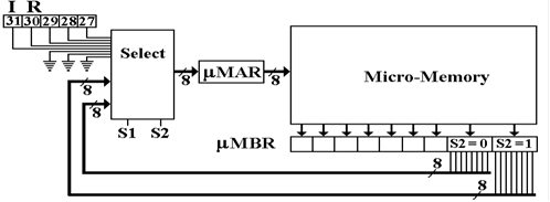
Summary
of Control Signals
This is a summary of control
signals, organized by bus and functional unit.
It is designed to support discussions of microprogramming, but can stand
on its own as a handy table.
|
Code |
Bus 1 |
Bus 2 |
Bus 3 |
ALU |
|
0 |
|
|
|
|
|
1 |
PC ®
B1 |
1 ®
B2 |
B3 ®PC |
tra1 |
|
2 |
MAR ®
B1 |
|
B3 ®
MAR |
tra2 |
|
3 |
R ®
B1 |
R ®
B2 |
B3 ®R |
shift |
|
4 |
IR ®
B1 |
|
B3 ®
IR |
not |
|
5 |
SP ®
B1 |
|
B3 ®
SP |
add |
|
6 |
|
MBR ®
B2 |
B3 ®
MBR |
sub |
|
7 |
|
IOD ®B2 |
B3 ®
IOD |
and |
|
8 |
|
|
B3 ®
IOA |
or |
|
9 |
|
|
|
xor |
|
10 |
|
|
|
|
Miscellaneous control signals Specified by the M1 and M2 fields
These fields are not encoded, so that each bit can be set separately. Each of M1 and M2 is a four bit field, having
bits Bit3, Bit2, Bit1, and Bit0.
Bit Number Shift Select Other Signals
Bit3 L / ![]() READ
READ
Bit2 A WRITE
Bit1 C extend
Bit0 0
® RUN
Micro-Code Format
The following assumes no more than
256 micro-words in the control store.
|
|
On |
Off |
|
|
|
Next
Address if |
||
|
Micro-Op |
B1 |
B2 |
B3 |
ALU |
M1 |
M2 |
Branch
= 0 |
Branch
= 1 |
|
4
bit |
4
bit |
4
bit |
4
bit |
4
bit |
4
bit |
4
bit |
8
bit |
8
bit |
Four–bit field format
|
Bit3 |
Bit2 |
Bit1 |
Bit0 |