Program
Execution
The program execution cycle is the basic Fetch / Execute cycle in
which the 32-bit instruction is fetched from the memory and executed. This cycle is based on two registers: PC the Program Counter –
a 20-bit address register
IR the Instruction Register – a 32-bit data register.
At the beginning of the instruction fetch cycle the PC contains the address of the instruction to be executed next. The fetch cycle begins by reading the memory at the address indicated by the PC and copying the memory into the IR. At this point, the PC is incremented by 1 to point to the next instruction. This is done due to the high probability that the instruction to be executed next is the instruction in the address that follows immediately; program jumps (BRU, BGT, etc.) are somewhat unusual, during these the PC might be given a new value by execution of the instruction.
All instructions share a common beginning to the fetch sequence. The common fetch sequence is adapted to the relative speed of the CPU and memory. We assume that the access time of the memory unit is such that the memory contents are not available on the step following the memory read, but on the step after that. Here is the common fetch sequence.
MAR ¬ PC send the address of the instruction to the memory
Read Memory this causes MBR ¬ MAR[PC]
PC ¬ PC + 1 cannot access memory, so might as well
increment the PC
IR ¬ MBR now the instruction is in the
Instruction Register.
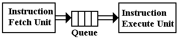
At this point, we note that the Boz–7 is simpler than most modern computers in that it lacks an instruction pre-fetch unit. If the design did include an instruction pre-fetch unit, that unit would independently fetch instructions and place them in an instruction queue for use by the execute unit, which might then fetch and execute an instruction in a single step. For such a design, the queue is implemented using a number of fast registers on the CPU chip.
When the instruction is in the IR, it is decoded and the common fetch sequence terminates. After this point, the execution sequence is specific to the instruction. This subsequent execution sequence includes calculation of the EA (Effective Address) for those instructions that take an operand. For the Boz–7, these are the LDR, STR, BR, and JSR instructions.
The next
step in the design of the CPU is to specify the microoperations
corresponding to the steps that must be executed in order for each of the
assembly language instructions to be executed.
Before considering these microoperations, we study several topics.
the structure of the bus or buses
internal to the CPU
the functional requirements on the
ALU
CPU Internal Bus Structure
We first consider the bus structure of the computer. Note that the computer has a number of buses
at several levels. For example, there is
a bus that connects the CPU to the memory unit and a bus that connects the CPU
to the I/O devices. In addition to these
important buses, there are often buses internal to the CPU, of which the
programmer is usually unaware. We now
consider the bus structure in light of the common fetch sequence.
PC ¬ PC + 1
This microoperation represents the incrementing of the PC to point to the next instruction on the probability that the next instruction will be the next to be executed. Note that this one microoperation places a functional requirement on the ALU – it must implement an addition operation. We shall use the notation add to denote the ALU addition operation (and the control signal that causes that ALU operation) and the all uppercase ADD to denote the assembly language operation.
At this point, we know that there must be at least one bus internal to the CPU so that the contents of the PC can be transferred to the ALU and the incremented value copied back to the PC. We consider a one bus solution and immediately notice a problem. The ALU must have two inputs for the add operation, one for the value of the PC and one for the value 1 used to increment the PC. If we use a single bus solution, we must allow for the fact that only one value at a time may be placed on the bus. We now present a design based on the single bus assumption.
 One
design would add an increment primitive for the ALU, but we avoid that complexity
and base our solution on the add operation only. We need a source of the constant 1, so we
create a “1 register” to hold the number.
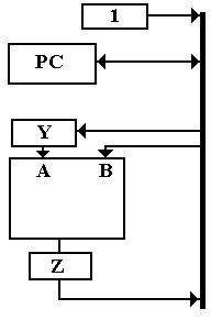
We postulate a two input ALU with a register Z to hold the output. Since the bus can have only one value at a
time, we must have a temporary register Y to hold one of the two inputs to the
ALU. Here are the microoperations.
One
design would add an increment primitive for the ALU, but we avoid that complexity
and base our solution on the add operation only. We need a source of the constant 1, so we
create a “1 register” to hold the number.
We postulate a two input ALU with a register Z to hold the output. Since the bus can have only one value at a
time, we must have a temporary register Y to hold one of the two inputs to the
ALU. Here are the microoperations.
CP1: 1 ® Bus, Bus ® Y
CP2: PC ® Bus, add // Result cannot be placed on bus
CP3: Z ® Bus, Bus ® PC // Bus is now available
We note that the single bus solution is rather slow. We would like another way to do this, preferably a faster one.
The solution we use is to have
three buses in the CPU, named B1, B2, and B3.
With three buses, we can put one value on each of two buses that serve
as input to the ALU and copy the results on the third bus, serving as input to
the PC, as follows
PC ® B1, 1 ® B2, add,
B3 ®
PC
More Implications of the Above Design
We now discuss explicitly a number of issues that arise as a direct
result of the desire to implement the operation to increment the PC as a single
simple addition operation, with microinstructions as shown above and repeated
here.
PC ® B1, 1 ® B2, add, B3 ® PC
Timing Constraints
The first requirement is that the CPU be fast enough to accomplish the
operations in the time allowed. A
detailed examination of a clock pulse will show the timing requirements.
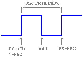
Figure: Timing Imposed by a Single Clock
Cycle
The figure
above attempts to show the constraints.
The contents of the PC are placed on bus B1 and the contents of the
constant register +1 are placed on bus B2 some time after the rise of the clock
pulse. Before the rise of the next clock
pulse, the new contents for the PC must have been transferred into that
register. Note the number of things that
must happen within this clock cycle:
1. The
contents of the PC and the +1 register must be placed on the two buses,
2. The
ALU must have added the contents of its two input buses,
3. The
ALU must have placed the results of the addition on its output bus B3, and
4. The
contents of B3 must have been transferred into the PC and become stable there.
We now see where the clock rate of a computer comes from. We want the clock rate to be as high as possible so the computer can be as fast as possible. Nevertheless, the clock rate must be slow enough to allow for transfers on the buses and for computation by the ALU. As an example, suppose that the ALU requires 2 nanoseconds to complete its computation. If we allow the CPU one–half cycle to do its work, that means that the whole cycle time cannot be shorter than 4 nanoseconds, and the clock rate cannot exceed 250 megahertz.
The Use of Master–Slave Registers
Note that the contents of the PC are incremented within the same clock
pulse. As a direct consequence, the PC
must be implemented as a master–slave flip–flop; one that responds to its input
only during the positive phase of the clock.
In the design of this computer, all registers in the CPU will be
implemented as master–slave flip–flops.
The Three-Bus Structure
As mentioned above, the design of a CPU with three internal data buses
allows a more efficient design. We name
the buses B1, B2, and B3. The use of
these buses is as follows: B1 and B2
are input to the ALU
B3 is an output from the ALU
Put another way: B3 is the source for all data going to each register. Each special–purpose register outputs data to one of bus B1 or bus B2. We allocate these registers to buses based partially on chance and partially on the requirement to avoid conflicts; if two data need to be sent to the ALU at the same time they need to be assigned to different buses. When we introduce the eight general–purpose registers, we specify that each of those can output to either bus B1 or bus B2. At times such a register feeds B1, and at other times it feeds B2.
What does the ALU require? The only way to determine what must be placed on each input bus is to examine each assembly language instruction, break it into microoperations, and allocate the bus assignments based on the requirements of the microoperations.
Common Fetch Sequence
We repeat the main
steps in the common fetch sequence
MAR ¬ PC send the address of the instruction
to the memory
Read Memory this
causes MBR ¬ MAR[PC]
PC ¬ PC + 1 cannot access memory, so might as
well increment the PC
IR ¬ MBR now the instruction is in the
Instruction Register.
This sequence of four
microoperations gives rise to a remarkable number of requirements for both the
ALU and the bus assignments. We first
examined the simple microoperation
PC ¬ PC + 1
and investigated the design implications of the requirement to execute this efficiently.
We have already noted the requirement that the ALU have an add control signal associated with the eponymous ALU primitive operation (use your dictionary). We have also noted the requirement that the ALU have two input buses and one output bus, in order to produce the output within one clock cycle.
If the ALU
is to produce the sum (PC + 1) in one clock pulse, the PC and the +1 register
must be allocated to different buses.
The CPU has two buses for input to the ALU: B1 and B2. We allocate the PC to one and, necessarily,
the +1 register to the other. We make the
bus allocations as follows
The PC is allocated to B1, in that
it outputs an address to B1.
At this moment the allocation is
arbitrary.
We allocate the constant +1 to B2, because it is the other available bus. In this 32–bit design, such a register has bit 0 connected to voltage and all other bits connected to ground.
As an aside
at this point, we have noted that B3 is used to transfer the results of the
addition into the PC. As noted above,
the complete set of control signals we have specified is
PC ® B1, 1 ® B2, add,
B3 ®
PC
The Primitives For Data Transfer
We now consider the implication of the microoperation MAR ¬
PC. We have noted that the PC outputs to
B1 and that B3 is used to transfer data to all registers. We now consider possibilities for
transferring the contents of the PC to the MAR.
One possibility would be for a direct transfer via a data bus dedicated to communication between the Program Counter and the Memory Address Register. Experience in the design of computers and their control units has shown that a direct–connect design is overly complex (see the appendix to this chapter) and that it is better to minimize dedicated data paths and maximize the use of common buses. The design of the Boz–7 follows this approach and uses the three data buses as a shared way to communicate between most of the registers in the CPU. As mentioned earlier, these are B1, B2, and B3.
We have
specified the three buses (B1, B2, and B3) in terms of their functionality for
the ALU. Let us now define them as used
by the registers in the CPU:
1. Buses
B1 and B2 communicate data from the registers to the ALU, and
2. Bus
B3 communicates data from the ALU to the registers.
Under this design approach, all transfers between any two registers must be passed through the ALU. Specifically this necessitates control signals to connect the buses that input into the ALU (B1 and B2) to the bus that outputs from the ALU (B3). This leads to the definition of ALU primitives to affect the transfer between buses.
We define
the two ALU primitives for data transfer
tra1 transfer the contents of B1 to B3
tra2 transfer the contents of B2 to B3.
Under this design, the only way for data to get to B3 from B1 is via the ALU. Thus, the requirement to transfer the contents of the PC to the MAR gives rise to the control signals
PC ® B1, tra1, B3 ® MAR
This is read as “place the PC contents on bus B1, connect bus B1 to bus B3, and then copy the contents of bus B3 into the MAR”.
Since we have mentioned the Memory Address Register, we might as well allocate it a bus so that it can send data to the ALU. We arbitrarily allocate the MAR to bus B1.
We now examine the last microoperation IR ¬ MBR. We assign the MBR to B2, thus requiring the tra2 primitive, already defined. At this point, we review what we have discovered from these four microoperations by converting them to control signals.
MAR ¬ PC PC ® B1, tra1, B3 ® MAR
Read Memory READ
PC ¬ PC + 1 PC ® B1, 1 ® B2, add,
B3 ®
PC
IR ¬ MBR MBR ® B2, tra2, B3 ® IR
For reasons that will become obvious later, we assign the IR to the bus not assigned to the MBR. As the MBR outputs to bus B2, we allocate the IR to bus B1.
Notation for Control Signals
Microoperations correspond to basic steps in program execution that can be
executed in one clock pulse. Control
signals correspond to those discrete signals that actually cause the microoperations
to have effect. We discussed the
difference above, when we mentioned the possibility of a control signal IR ¬ MBR
to implement the microoperation IR ¬ MBR. Control
signals are named for the action that each enables; microoperations may
correspond to a sequence of control signals that all can be asserted in
parallel during one clock pulse.
Consider the following three control signal sequences. They are identical, in that each has the same interpretation and causes the same actions to take place.
MBR ® B2, tra2, B3 ® IR.
B2 ¬
MBR, tra2, IR ¬ B3.
IR ¬
B3, tra2, B2 ¬ MBR.
We use whatever notation that is most convenient. This author prefers the first notation, and will use it almost exclusively. Students may use any of the three, if the use is consistent.
A First Look At The CPU and Its Buses
We now look at the CPU design as it has evolved to this point in response
to the requirements imposed by the common fetch sequence.
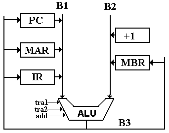
Figure: Partial
CPU Design
Note that the buses B1 and B2 are shown as input to the ALU and that the divided bus B3 is shown as output from the ALU. The convention of drawing bus B3 this way, coming down from the ALU and dividing into two parts, is a convention to facilitate drawing the figures and has no particular significance otherwise.
Another Look at the IR (Instruction
Register)
We now note that the IR does not communicate with bus B1 in the same
way as other registers communicate with the bus structure. In order to understand this difference, we
must examine the structure of the IR; specifically what data are placed into
it.
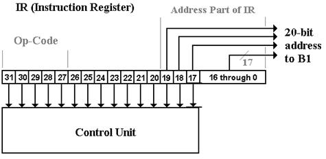
Figure: Different
Allocations of Bits in the Instruction Register
At this point, the important fact is that only the low order 20 bits are transferred to bus B1. This is due to the fact that only the low order 20 bits are interpreted as an address or data; other bits signify the op–code and other control information, such as register selection. In other words, the only part of the Instruction Register that is passed to the bus system is that part that is used in address computation or as data for the immediate operands. The bits that are used to determine the operation and select registers are passed directly to the control unit.
The reader will note that bits 19 through 17 of the IR are sent to both bus B1 and to the control unit. This is not a duplication, but a simplification in the design. When those bits are used as an address part, the control unit will make no use of them. When they are used by the control unit, they will specify a register number in an instruction that does not use addresses. Bottom line: we may use bits in a register for several distinct purposes.
We now address the issue of how
to transfer 20 bits via a 32–bit bus.
There are two options: as a sign extended 20–bit two’s–complement
integer, or as 32 individual bits with the 20 high order bits set to 0. In order to understand this decision, we
examine the seven instructions that will involve one of these transfers. The instructions are the following.
LDI Load
the (sign extended) value of IR19-0 into the 32–bit register.
This allows
loading negative values in the range ( – 219) to ( – 1).
ANDI Use
the 20 bits in IR19-0 as a 20–bit Boolean mask for logical AND with
the contents of
the 32–bit register. At present, this is
not sign–extended.
ADDI Add
the (sign extended) value of IR19-0 to the 32–bit register.
This allows
subtraction of constant numbers.
LDR Use
the unsigned value of IR19-0 to compute a memory address.
STR Use
the unsigned value of IR19-0 to compute a memory address.
BR Use
the unsigned value of IR19-0 to compute a memory address.
JSR Use
the unsigned value of IR19-0 to compute a memory address.
We use a
control signal “Extend” to determine
how to interpret the 20 low–order bits found in the Instruction Register. The interpretation of this signal is as
follows:
1) If
Extend = 1, the value of IR19-0
is treated as a 20–bit two’s–complement integer
and
sign extended into a 32–bit two’s–complement integer.
2) If
Extend = 0, the value of IR19-0
is treated as a 20–bit unsigned integer and
0000
0000 0000 ¢ IR19-0 is transferred to the bus.
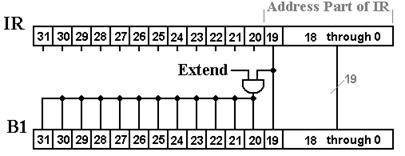
Figure: Communicate the IR to the Bus
General Purpose Register File
We now add the eight general purpose registers to the mix, specifying that
each can feed either bus B1 or bus B2.
Note that constant register %R0 has no input from bus B3.
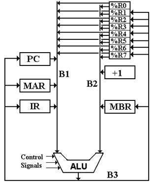
Figure: Add the
General Purpose Registers
Add The Other Registers
Before we continue, it is prudent to add the other
registers to the bus diagram of the CPU.
The other registers are introduced now because this author cannot think of a
better place to do it. Each of the new
registers will be explained at the appropriate time, although all have been discussed
briefly in the chapter on the Instruction Set Architecture.
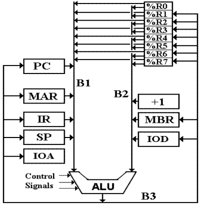
Figure: The Complete Register Set of the
Boz–7
There are four new registers introduced
here.
SP the
Stack Pointer, used in calling subroutines and returning from them.
Subroutine calls will PUSH
the return address onto the stack, and subroutine
returns will POP the
return address from the stack. Future
revisions in this
design might add user–callable
PUSH and POP to the Instruction Set Architecture.
+ 1 the
“plus one” constant register is used to increment the SP (Stack Pointer) on
POP and to increment the
PC (Program Counter) during the fetch cycle.
Since
the Boz–7 can subtract,
this also decrements the SP on PUSH.
IOA the 16–bit address used to select the I/O register.
IOD the 32–bit register used for I/O data, either input or output.
We are about to discuss addressing modes as used to access computer memory. In the current design, these do not apply to I/O device registers, which are directly addressed. The only reason for this choice is simplicity of design.
Two Addressing Modes:
Direct and Indexed
We shall soon consider all four addressing modes. For now, we consider the impact of two of the
addressing modes on the CPU design.
Recall that the address part of the register load and store instructions
occupies the lower 20 bits: bits 19 through 0 inclusive. When a LDR (Load Register) or STR (Store
Register) instruction is copied into the Instruction Register, the address part
is IR19–0. In direct addressing,
this is the address to use. In indexed
addressing, the address to use is IR19–0 + (R), where (R) denotes
the contents of the register specified in IR22-20 to be used as an
index register. These addresses go to
the MAR, thus
Direct Addressing MAR
¬ IR19–0
Indexed Addressing MAR ¬
IR19–0 + (R)
At this
point, we mention the trick with register 0, actually a standard design
practice. Consider the above two
descriptions, slightly rewritten.
IR22IR21IR20
= 000 MAR ¬ IR19–0 + 0
IR22IR21IR20
= 001 MAR ¬ IR19–0 + (%R1)
IR22IR21IR20
= 010 MAR ¬ IR19–0 + (%R2)
IR22IR21IR20
= 011 MAR ¬ IR19–0 + (%R3)
IR22IR21IR20
= 100 MAR ¬ IR19–0 + (%R4)
IR22IR21IR20
= 101 MAR ¬ IR19–0 + (%R5)
IR22IR21IR20
= 110 MAR ¬ IR19–0 + (%R6)
IR22IR21IR20
= 111 MAR ¬ IR19–0 + (%R7)
The trick is to define register %R0 as a constant register containing the constant value 0. With this new design consideration, the microoperation MAR ¬ IR19–0 becomes the same as MAR ¬ IR19–0 + (%R0). The advantage of this trick is that the control unit is considerably simplified – always a good thing. As a result, we have only two design options at the control signal level: indexed and indexed-indirect. The effect is given in the following table.
|
|
Indexed by %R0 |
Indexed by another register |
|
Indirection Not Used, IR26 = 0 |
Direct |
Indexed |
|
Indirection Used, IR26 = 1 |
Indirect |
Indexed-Indirect |
Attaching the General-Purpose Registers
to the Three Buses
The next step here is to decide how to attach the general purpose registers
to the bus structure. To do this, we use
selectors and control signals. The
selectors are three-bit signals generated based on bits in the Instruction
Register.
B1S Bus 1 Source, a 3-bit selector
specifying the register to place on bus B1
when the control signal
R ®
B1 is asserted by the control unit.
B2S Bus 2 Source, a 3-bit selector
specifying the register to place on bus B2
when the control signal
R ®
B2 is asserted by the control unit.
B3D Bus 3 Destination, a 3-bit selector
specifying the register to copy the contents
of bus B3 when the
control signal B3 ®
R is asserted by the control unit.
Here is the figure showing how the eight general purpose registers are connected to the three buses B1, B2, and B3. For simplicity, only a single bit is shown.
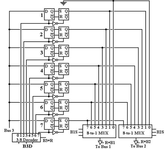
Figure: Connecting
a Single Bit of Each Register to the Buses
Note that the enable input of the 3-to-8 decoder is connected to the signal B3 ® R. When this signal is asserted, the contents of the three-bit selector signal B3D determine which register is to receive the contents of bus B3 and the clock input of each flip-flop in that register is pulsed, thus loading the register. Note that output 0 of the decoder goes nowhere, corresponding to the fact that register %R0 is a constant register that cannot be loaded.
The
three-bit selector signals B1S and B2S are always active, so that each of the
two 8-to-1 multiplexers always has an output.
Each of these outputs is transferred to the corresponding bus only when
the corresponding control signal is asserted.
For example, we might have
B1S = 011, but %R3 is placed on the bus if and only if R ® B1 =
1. If R ® B1 = 0, either a
special-purpose register, such as the IR, is being placed on bus B1 or the bus
is not active.
The three–bit selectors B1S, B2S, and B3D are related to the bit fields found in the IR, but not identical to them due to the structure of the instruction set. In order to determine how to generate these three selectors, we must look at the structure of each assembly language instruction that references a general purpose register.
Generation of the Bus Select Signals
B1S, B2S, and B3D
We now examine the instruction set to determine how we generate the
three–bit selectors B1S, B2S, and B3D.
These three 3–bit selectors are associated with bits in the IR. In general, the association of these
selectors with bits in the Instruction Register (IR) is quite
straightforward. For many instructions,
the fields are uniformly specified as follows.
|
31 |
30 |
29 |
28 |
27 |
26 |
25 |
24 |
23 |
22 |
21 |
20 |
19 |
18 |
17 |
16 – 0 |
|
Op Code |
I bit |
Destination Register |
Source Register 2 |
Source Register 1 |
Not used |
||||||||||
The
general rule is that B3D is
determined by bits 25 – 23 of the Instruction Register
B2S
is determined by bits 22 – 20 of the Instruction Register
B1S
is determined by bits 19 – 17 of the Instruction Register
We shall soon note a number of variations on this basic format, which is based on the binary register–to–register operations. We begin with a few observations.
1) Bits
19 – 0 of the Instruction Register are used by some instructions in address
computation. For these instructions, the selector B1S is
not used.
2) We
shall provide hardware for generating the selectors even when they are not
used. This is much simpler than any restriction
based on usage.
3) The
instructions that do compute argument addresses can use indexed addressing,
in which the contents of a
general–purpose register (including %R0) are added to
an address from the IR19-0
to compute an effective address. Indexed
addresses will
be computed using the
following sequence of control signals.
IR19-0 ® B1, R ® B2, add, B3 ® MAR.
4) The
one exception to the “general rule” is the STR (Store Register) instruction, in
which the register denoted by
bits 25 – 23 of the IR must be used for the source
register. For this instruction, bits 25 – 23 of the IR
determine the value of B1S, and
B3D is not used. Since the 3–bit value B3D is not used, it is
also set to IR25-23.
As the last statement might seem a bit abstract and even arbitrary, we shall examine it in a bit more detail. In order to do this, we must look ahead and notice the format of the instruction.
The STR Instruction
|
31 |
30 |
29 |
28 |
27 |
26 |
25 |
24 |
23 |
22 |
21 |
20 |
19 – 0 |
|
0 |
1 |
1 |
0 |
1 |
I bit |
Source Register |
Index Register |
Address |
||||
This is the only instruction for which bits 25 to 23 contain a source register. Normally these bits specify the destination for bus 3 (that is the selector B3D). As there is no destination register for this instruction, the control signal B3 ® R is never asserted, and there is no need to suppress generation of the selector B3D. The source register must be copied to either bus B1 or bus B2, as those two buses are the only way to communicate data from a register to the ALU. However bus B2 is “claimed” by the index register, so we use bus B1.
Immediate Addressing
|
31 |
30 |
29 |
28 |
27 |
26 |
25 |
24 |
23 |
22 |
21 |
20 |
19 – 0 |
|
Op–Code |
|
Destination Register |
Source |
Immediate Argument |
||||||||
Op–Code 00000 HLT Halt (Does not use
addressing)
00001 LDI Load
Immediate (Does not use Source
Register)
00010 ANDI Immediate
logical AND
00011 ADDI Add
Immediate
In these instructions, the source register most commonly will be the same as the destination register. While there is some benefit to having a distinct source register, the true motivation for this design is that it simplifies the logic of the control unit. For these four instructions, the contents of IR25-23 will always be interpreted as a destination register (generate B3D) and the contents of IR22-20 will always be interpreted as a source register (generate B2S).
The most common immediate
instructions will probably be the following.
LDI %RD, 0 --
Load the register with a 0.
LDI %RD, 1 --
Load the register with a 1
ADDI %RD, %RD,
1 -- Increment the register
ADDI %RD, %RD, – 1 --
Decrement the register
A Gap in the Op–Codes
Op–Codes 00100 (0x04), 00101 (0x05), 00110 (0x06), and 00111 (0x07) are
presently not assigned. This gap has
been introduced in order to facilitate design of the control unit.
Input/Output Instructions
The design calls for isolated I/O, so it has dedicated input and output
instructions. A memory–mapped I/O design
would skip the GET and PUT, having dedicated I/O addresses.
Input
|
31 |
30 |
29 |
28 |
27 |
26 |
25 |
24 |
23 |
22 |
21 |
20 |
19 |
18 |
17 |
16 |
15 – 0 |
|
0 |
1 |
0 |
0 |
0 |
|
Destination |
Not Used |
Not Used |
I/O Address |
|||||||
Output
|
31 |
30 |
29 |
28 |
27 |
26 |
25 |
24 |
23 |
22 |
21 |
20 |
19 |
18 |
17 |
16 |
15 – 0 |
|
0 |
1 |
0 |
0 |
1 |
|
Not Used |
Source |
Not Used |
I/O Address |
|||||||
Note that these two instructions use different fields to denote the register affected. This choice will simplify the control circuit. All unused bits are assumed to be 0, but need not be as these bits will be ignored by the control unit.
Return from Subroutine /
Return from Interrupt.
|
31 |
30 |
29 |
28 |
27 |
26 – 0 |
|
Op–Code |
Not Used |
||||
Op–Code = 01010 RET Return
from Subroutine
01011 RTI Return
from Interrupt (Not presently implemented)
Neither of these instructions takes an argument or uses an address, as the appropriate information is assumed to have been placed on the stack.
Memory Addressing
The next four instructions (LDR, STR, JSR, and BR) can use memory addressing. The first two use the memory address for a data copy between a specific register and memory. The next two use the memory address as the target location for a jump.
The generic structure of these instructions is as follows.
|
31 |
30 |
29 |
28 |
27 |
26 |
25 |
24 |
23 |
22 |
21 |
20 |
19 – 0 |
|
Op Code |
I bit |
Register/Flags |
Index |
Address |
||||||||
The contents of bits 25 – 23 depends on the instruction.
The Real Reason for
%R0 º 0
We now discuss an addressing trick that is one of the real reasons that we have included a general–purpose register that is identically 0. What we are doing is simplifying the control unit by not having to process non-indexed addressing; that is, direct or indirect. Note that bits 22 – 20 of the IR specify the index register to be used in address calculations.
When the I-bit (bit 26) is zero, we will call for indexed addressing, using the specified
register. Thus the effective address is
given by EA = Address + (%Rn), where %Rn is the register specified in bits 22 –
20 of the IR. But note the following
If Bits 22 – 20 = 0, we have
%R0 and EA = Address + 0, thus a direct address.
When the I-bit is 1, we have the same convention. Indexed by %R0, we have indirect addressing, and indexed by another register, we have indexed-indirect addressing.
The “bottom line” on these addresses is shown in the table below.
|
|
IR22-20 = 000 |
IR22-20 ¹ 000 |
|
IR26 = 0 |
Indexed by %R0 (Direct) |
Indexed |
|
IR26 = 1 |
Indirect, indexed by %R0 (Indirect) |
Indexed-Indirect |
Load Register
|
31 |
30 |
29 |
28 |
27 |
26 |
25 |
24 |
23 |
22 |
21 |
20 |
19 – 0 |
|
0 |
1 |
1 |
0 |
0 |
I bit |
Destination Register |
Index Register |
Address |
||||
Here the I bit can be considered part of the opcode, if
desired.
011000 Load the register using direct or indexed addressing
011001 Load the register using indirect or indexed-indirect
addressing
For a load register operation, bits 25 – 23 specify the destination register. If the destination register is %R0, no register will change value. While this seems to be a “no operation”, it does set the condition codes in the PSR and might be used solely for that effect. We note here that such a programming trick is recommended in a number of text books.
Store Register
|
31 |
30 |
29 |
28 |
27 |
26 |
25 |
24 |
23 |
22 |
21 |
20 |
19 – 0 |
|
0 |
1 |
1 |
0 |
1 |
I bit |
Source Register |
Index Register |
Address |
||||
Here the I bit can be considered part of the opcode, if
desired.
011010 Store the register using direct or indexed addressing
011011 Store the register using indirect or indexed-indirect
addressing.
For a store register operation, bits 25 – 23 specify the source register. If the source register is %R0, the memory at the effective address will be cleared.
Subroutine Call
|
31 |
30 |
29 |
28 |
27 |
26 |
25 |
24 |
23 |
22 |
21 |
20 |
19 – 0 |
|
0 |
1 |
1 |
1 |
0 |
I bit |
Not Used |
Index |
Address |
||||
Here the I bit can be considered
part of the opcode, if desired.
011100 Call subroutine using direct or indexed addressing
011101 Call subroutine using indirect or indexed-indirect
addressing
An earlier design of this computer used conditional subroutine calls, with bits 25 – 23 of the instruction specifying a condition, as they do for the BR instruction. This was rejected as both overly complex and not reflected in the design of commercial computers. All JSR instructions are unconditional; the subroutine is always called.
To create code for a conditional
call to a subroutine, just pair the JSR instruction with a conditional BR
instruction, as in the following sequence.
BLT IsNeg, 0
JSR IsNotNeg
Subroutine Linkage
Later in this chapter, we shall define the control signals for both the subroutine call (JSR) instruction and the subroutine return (RET) instruction. At this point, we must specify the convention to be used, as the two instructions must be designed as a pair.
When a subroutine or function is
called, control passes to that subroutine but must return to the instruction
immediately following the call when the subroutine exits. There are two main issues in the design of a
calling mechanism for subroutines and functions. These fall under the heading “subroutine linkage”.
1. How to pass the arguments to the subroutine.
2. How to pass the return address to the subroutine so that,
upon completion,
it returns to the correct address.
A function is just a subroutine that returns a value. For functions, we have one additional issue in the linkage discussion: how to return the function value.
The discussion in this chapter will assume some appropriate mechanism for passing the arguments to the subroutine, and an appropriate way to return the function value. The consideration here is the proper handling of the return address.
In order to understand the full subroutine calling mechanism, we must first understand its context. We begin with the situation just before the JSR completes execution. In this instruction, we say that EA represents the address of the subroutine to be called. The last step in the execution of the JSR is updating the PC to equal this EA. Prior to that last step, the PC is pointing to the instruction immediately following the JSR. This is due to the automatic updating of the PC for every instruction in (F, T1).
The execution of the JSR involves three tasks:
1. Computing the value of the Effective Address (EA).
2. Storing the current value of the
Program Counter (PC)
so that it can be
retrieved when the subroutine returns.
3. Setting the PC = EA, the address of the subroutine or function.
The simplest method for storing
the return address is to store it in the subroutine itself. A typical mechanism, such as used by the
CDC–6600, allocates the first word of the subroutine to store the return
address. If the subroutine is at address
Z in a word–addressable machine such as the Boz–7, then
Address Z holds the return address.
Address (Z + 1) holds the first executable instruction
of the subroutine.
BR
*Z An indirect
jump on Z is the last instruction of the subroutine.
Since
Z holds the return address, this affects the return.
This is a very efficient mechanism. The difficulty is that it cannot support recursion.
Example:
Non–Recursive Call
Suppose the following instructions
100 JSR 200
101 Next Instruction
200 Holder for Return Address
201 First Instruction
Last BR *200
After the subroutine call, we would have
100 JSR 200
101 Next Instruction
200 101
201 First Instruction
Last BR *200
The BR*200 would cause a branch to address 101, thus causing a proper return.
Example 2: Using This
Mechanism Recursively
Suppose a five instruction subroutine at address 200. Address 200 holds the return address and addresses 201 – 205 hold the code. This subroutine contains a single recursive call.
Called from First
Recursive First
address 100 Call Return
200 101 200 204 200 204
201 Inst 1 201 Inst 1 201 Inst 1
202 Inst 2 202 Inst 2 202 Inst 2
203 JSR 200 203 JSR 200 203 JSR 200
204 Inst 4 204 Inst 4 204 Inst 4
205 BR * 200 205 BR * 200 205 BR * 200
Note that the first recursive call overwrites the stored return address for the main routine. As long as the subroutine is returning to itself, there is no difficulty. It will never return to the original calling routine. The solution to this problem is to use a stack for the return address.
Following standard practice, the Boz–7 has been revised to have the stack grow towards smaller addresses when an item is added. Given this we have two options for implementing PUSH, each giving rise to a unique implementation of POP.
Option PUSH X POP Y
1 M[SP]
= X SP = SP + 1 // Post–decrement on PUSH
SP = SP – 1 Y = M[SP]
2 SP
= SP – 1 Y = M[SP] // Pre–decrement on PUSH
M[SP] = X SP = SP + 1
The constraints on memory access
dictate the first option.
Post–decrement on PUSH must be paired with pre–increment on POP.
The operation M[SP] = X
corresponds to a memory write. The
latest time at which
this can be done is (E, T2), due to the requirement of a wait cycle before (F,
T0).
If (E, T2) corresponds to M[SP] = X,
then (E, T3) can correspond to SP = SP
– 1. This does not affect memory.
Branch
|
31 |
30 |
29 |
28 |
27 |
26 |
25 |
24 |
23 |
22 |
21 |
20 |
19 – 0 |
|
0 |
1 |
1 |
1 |
1 |
I bit |
Branch |
Index |
Address |
||||
Here the I bit can be considered
part of the opcode, if desired.
011110 Branch using direct or indexed addressing
011111 Branch using indirect or indexed-indirect addressing
The branch condition code field determines under which conditions the Branch instruction is executed. The conditions used are based on the condition codes found in the Program Status Register, the results of the last arithmetic operation. The eight possible options are.
Condition Action
000 Branch Always (Unconditional Jump)
001 Branch on negative result
010 Branch on zero result
011 Branch if result not
positive
100 Branch if carry–out is 0
101 Branch if result not
negative
110 Branch if result is not
zero
111 Branch on positive result
The alert reader will note that most of the condition codes come in pairs; with one exception condition code “1xy” specifies the opposite of condition code “0xy”. This facilitates the design of the hardware to generate the signal “Branch” that will actually determine if the branch is to be taken.
Some authors have taken this symmetry to an extreme, thus having condition 000 for “branch always” and condition “100” for “Not (branch always)”; i.e., “branch never”. The designer of this computer has dismissed the “branch never” instruction as nonsense, and looked around for another useful condition. The best he can do is to select a condition that will facilitate multiple–precision arithmetic.
We shall here anticipate a design decision that will speed up the CPU. There are two options for conditional branches: either the branch is to be taken or it is not to be taken. This will depend on the value of a signal, called “Branch”, that will be generated from the status bits in the PSR (Program Status Register) and the condition codes, listed above.
If Branch = = 1, the branch is always taken. This is always true for condition code 0.
If Branch =
= 0, the branch is not taken. This can
be the case when the condition code is
not 0 and the condition required for branching is not satisfied. When this is the case, the control unit will
proceed to fetch the instruction following the branch instruction, and not
waste cycles computing an address that is guaranteed not to be used.
We shall see that this action is controlled by the Major State Register, which will be defined in due time.
Binary
Register-To-Register
|
31 |
30 |
29 |
28 |
27 |
26 |
25 |
24 |
23 |
22 |
21 |
20 |
19 |
18 |
17 |
16 – 0 |
|
Op–Code |
|
Destination Register |
Source Register 2 |
Source Register 1 |
Not used |
||||||||||
Here the bits IR25-23
specify a destination register and each of IR22-20 and IR19-17
specify a source register. Here the
assignments appear obvious:
B3D = IR25-23, B2S = IR22-20, and
B1S = IR19-17.
Note that subtraction with the destination register set to %R0 becomes a comparison to set the condition codes for a future branch operation.
Opcode
= 10101 ADD Addition
10110 SUB Subtraction
10111 AND Logical
AND
11000 OR Logical
OR
11001 XOR Logical
Exclusive OR
Unary
Register-To-Register
|
31 |
30 |
29 |
28 |
27 |
26 |
25 |
24 |
23 |
22 |
21 |
20 |
19 |
18 |
17 |
16 |
15 |
14 – 0 |
|
Op–Code |
|
Destination Register |
Source Register |
Shift Count |
Not Used |
||||||||||||
Here bits IR25-23 specify a destination register and IR22-20 specify a source register. In previous instructions, we have used IR22-20 to specify the control B2S, so we continue the practice. Thus we have B3D = IR25-23 and B2S = IR22-22.
Note that bus B1 is not used by these instructions. To simplify the control unit, we arbitrarily make the assignment B1S = IR19–17, even though the assignment will not be used.
Opcode
= 10000 LLS Logical
Left Shift
10001 LCS Circular
Left Shift
10010 RLS Logical
Right Shift
10011 RAS Arithmetic
Right Shift
10100 NOT Logical
NOT (Shift count ignored)
NOTES: 1. If
(Count Field) = 0, a shift operation becomes a register move.
2. If (Source Register = 0), the operation
becomes a clear.
3. Circular right shifts are not supported,
because they may be implemented
using circular
left shifts. A right circular shift by N
bits (0 £
N £
31) may
be implemented as a circular left shift by (32 – N) bits. No bits are lost.
4. The shift count, being a 5 bit number, has
values 0 to 31 inclusive.
5. When the control unit is processing the NOT
signal, bits 19 – 0 of the IR
are ignored. Specifically,
the field called “shift count” is not used.
6. The use of a variable or register to hold the
shift count is not supported by this
microarchitecture. Use a looping structure with repeated shifts
to do this.
Summary
The following table summarizes the requirements levied by the
instructions on the generation of the control signals B1S, B2S, and B3D.
|
|
B1S |
B2S |
B3D |
|
HLT |
|
|
|
|
LDI |
|
|
IR25-23 |
|
ANDI |
|
IR22-20 |
IR25-23 |
|
ADDI |
|
IR22-20 |
IR25-23 |
|
GET |
|
|
IR25-2 |
|
PUT |
|
IR22-20 |
|
|
LDR |
|
IR22-20 |
IR25-23 |
|
STR |
IR25-23 |
IR22-20 |
|
|
BR |
|
IR22-20 |
|
|
JSR |
|
IR22-20 |
|
|
RET |
|
|
|
|
RTI |
|
|
|
|
Unary Register |
|
IR22-20 |
IR25-23 |
|
Binary Register |
IR19-17 |
IR22-20 |
IR25-23 |
We now display a circuit that is compatible with these requirements.
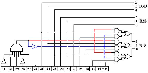
Figure: Generation of Selectors From the
IR
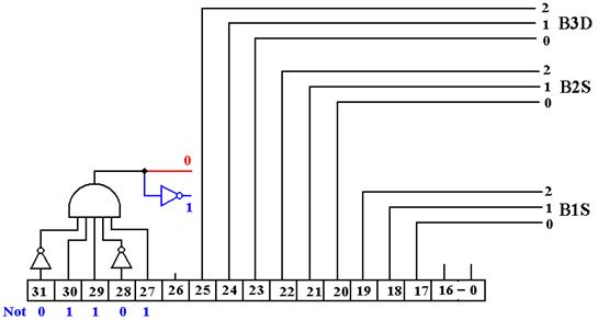
Note that B1S = IR25-23 for IR31-27 = 01101 and B1S = IR19-17 otherwise. This will give a value to B1S for a number of instructions that do not use bus B1, but this causes no trouble and yields a simpler control unit. Note that we always have B2S = IR22-20 and B3D = IR25-23.
A
Clarification
The figure above is a bit busy, so we shall give two different
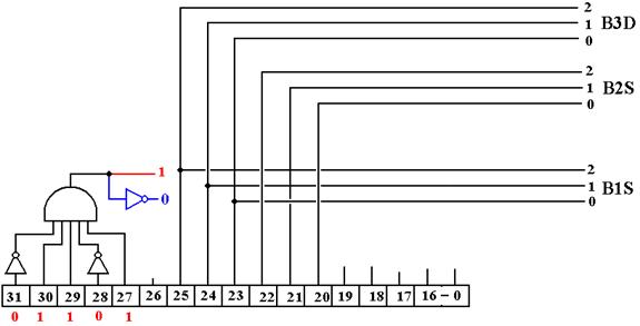
simplifications, one for the STR instruction and one for other instructions.
STR
Op–Code = 01101
Here is the effective circuit when IR31-27 = 01101.
The selector B3D is not used as the control signal B3 ® R is not asserted.
Other Op–Codes
Here is the effective circuit for other instructions.
Major States vs. Minor States
In this version of the design, the computer will have a control unit for the CPU based on three major states: Fetch, Defer, and Execute. We shall present two designs for the control unit: hardwired and microprogrammed. The hardwired control unit will be based on the major states, each containing four minor states, labeled T0, T1, T2, and T3. In the microprogrammed control unit, the major states will represent logical divisions of the microcode and the minor states will be present only by implication. The design will focus on “single state” execution, meaning that most instructions will execute in the “Fetch” major state, with only the memory-referencing instructions requiring Defer and Execute.
Control Signals
We now
present a discussion of the control signals for each of the instructions. We begin with a discussion of the common
fetch control signals.
F, T0: PC ® B1, tra1, B3 ® MAR, READ. // MAR ¬ (PC)
F, T1: PC ® B1, 1 ® B2, add, B3 ® PC. // PC ¬ (PC) + 1
F, T2: MBR ® B2, tra2, B3 ® IR. // IR ¬
(MBR)
In the above, the student should recall that the parentheses indicate the contents of a register. The notation is perhaps redundant, but we use “(PC)” to refer to the contents of the PC.
At this
point, the control unit will attempt to execute the instruction during the T3
phase of the Fetch major state. The only
instructions that cannot be executed in this time slot are those four
instructions that reference memory:
LDR memory address of the argument to be copied into a
general-purpose register,
STR memory address to receive the contents of a general-purpose
register,
BR memory address indicating the next instruction for execution,
and
JSR memory address indicating the location of the subroutine.
For these
three instructions only, the Fetch state is defined fully as follows.
F, T0: PC ® B1, tra1, B3 ® MAR, READ. // MAR ¬ (PC)
F, T1: PC ® B1, 1 ® B2, add, B3 ® PC. // PC ¬ (PC) + 1
F, T2: MBR ® B2, tra2, B3 ® IR. // IR ¬
(MBR)
F, T3: 000000000000 ¢ IR19-0 ® B1, R ® B2, add, B3 ® MAR.
The operation in F, T3 is the concatenation operator. Here twelve zeroes are appended to the 20-bit address from the IR to produce a full 32-bit address with the twelve high-order bits all set to 0. The hardware has been designed to append these 0 bits during the transfer.
Defer State
For these four instructions only, the control unit may cause execution of a
Defer state if the
“I bit” – IR26 is set to 1.
Here is the uniform code for the defer state. The reader will note the two WAIT
states. This is due to the fact that our
design calls for four minor states per major state and there is nothing else to
do in the defer state.
D, T0: READ. //
Address is already in the MAR.
D, T1: WAIT. //
Cannot access the MBR just now.
D, T2: MBR ® B2, tra2, B3 ® MAR. // MAR ¬ (MBR)
D, T3: WAIT.
Control Signals for the Boz–7
The control signals are listed in numeric order by Op-Code, with some general comments added as necessary to clarify the control signals.
HLT Op-Code = 00000 (Hexadecimal
0x00)
F, T0: PC
®
B1, tra1, B3 ®
MAR, READ. // MAR ¬ (PC)
F, T1: PC ® B1, 1 ® B2, add, B3 ® PC. // PC ¬ (PC) + 1
F, T2: MBR ® B2, tra2, B3 ® IR. // IR ¬
(MBR)
F, T3: 0 ® RUN. //
Reset the RUN Flip-Flop
LDI Op-Code = 00001 (Hexadecimal
0x01)
F, T0: PC
®
B1, tra1, B3 ®
MAR, READ. // MAR ¬ (PC)
F, T1: PC ® B1, 1 ® B2, add, B3 ® PC. // PC ¬ (PC) + 1
F, T2: MBR ® B2, tra2,
B3 ® IR. //
IR ¬ (MBR)
F, T3: IR ® B1, extend, tra1, B3 ® R. //
Copy IR19-0 as signed integer
In the next instructions, the source register most commonly will be the same as the destination register. While there is some benefit to having a distinct source register, the true motivation for this design is that it simplifies the logic of the control unit.
ANDI Op-Code
= 00010 (Hexadecimal
0x02)
F, T0: PC
®
B1, tra1, B3 ®
MAR, READ. // MAR ¬ (PC)
F, T1: PC ® B1, 1 ® B2, add, B3 ® PC. // PC ¬ (PC) + 1
F, T2: MBR ® B2, tra2, B3 ® IR. // IR ¬
(MBR)
F, T3: IR ® B1, R ® B2, and, B3 ® R. // Copy IR19-0 as 20
bits.
// The 20 bits IR19-0
are copied without extension, so we have in reality
// 0000 0000 0000
¢ IR19-0 ®
B1. This may be changed in a future
design.
ADDI Op-Code = 00011 (Hexadecimal
0x03)
F, T0: PC
®
B1, tra1, B3 ®
MAR, READ. // MAR ¬ (PC)
F, T1: PC ® B1, 1 ® B2, add, B3 ® PC. // PC ¬ (PC) + 1
F, T2: MBR ® B2, tra2, B3 ® IR. // IR ¬
(MBR)
F, T3: IR ® B1, R ® B2, extend, add,
B3 ®
R. // Add signed integer
A Gap in the Op–Codes
Op–Codes 00100 0x04
00101 0x05
00110 0x06
00111 0x07 are presently not assigned.
The next two instructions will have immediate action with regard to the Input / Output devices. These two instructions should be used only after the status of the I/O device has been tested and the device found to be ready for an I/O transaction.
At present the I/O Address Register, IOA, is a 16–bit register. In the transfer from the 32–bit bus B3, denoted by B3 ® IOA, only the 16 low order bits of the bus are copied.
The reader will note that (F, T3) for each of these instructions is a WAIT or NOP. This choice is made to isolate the I/O–specific code to the Execute phase. The reader will also note that neither instruction uses the Defer phase. This is due to the simplicity of generation of addresses for the I/O device registers; just put the value into IR15-0.
Another reason to leave (F, T3) as a NOP (No Operation) is that the design of the control unit for the FETCH state is already complex enough. If the instruction execution requires more than one microoperation, but not more than four, move them all to the EXECUTE state.
The
observant reader will also note that neither of these instructions is
particularly sophisticated, in that neither performs a number of important
checks. In particular, the GET operation
will input from the addressed register without regard to two important items:
1) that
the register actually exists and is an input register, and
2) that
the register actually has fresh data in it.
Similarly, the PUT operation will attempt to output data to nonexistent registers or registers that are for input only. In addition, there is no interlock to prevent this instruction from overwriting data previously sent out and not yet processed by the output device.
GET Op-Code = 01000 (Hexadecimal
0x08)
F, T0: PC
®
B1, tra1, B3 ®
MAR, READ. // MAR ¬ (PC)
F, T1: PC ® B1, 1 ® B2, add, B3 ® PC. // PC ¬ (PC) + 1
F, T2: MBR ® B2, tra2, B3
® IR. //
IR ¬ (MBR)
F, T3: NOP.
E,
T0: IR ® B1,
tra1, B3 ® IOA. //
Send out the I/O address
E, T1: WAIT.
E, T2: IOD ® B2, tra2, B3
®
R. // Get the
results.
E, T3: NOP.
PUT Op-Code = 01001 (Hexadecimal
0x09)
F, T0: PC
®
B1, tra1, B3 ®
MAR, READ. // MAR ¬ (PC)
F, T1: PC ® B1, 1 ® B2, add, B3 ® PC. // PC ¬ (PC) + 1
F, T2: MBR ® B2, tra2, B3
® IR. //
IR ¬ (MBR)
F, T3: NOP.
E,
T0: R ® B2, tra2, B3 ® IOD //
Get the data ready
E, T1: WAIT.
E, T2: IR ® B1, tra1, B3
®
IOA. // Sending
out the address
E, T3: NOP. //
causes the output of data.
The timing assumptions for the PUT operation may soon be revised, but for the moment it is assumed that data are placed into the output data register as soon as its address is placed into the register IOA, and thus onto the I/O address bus.
Subroutine Call and Return
The Boz–7 provides the stack–based mechanisms for subroutine call and
return that are required to support recursive subroutine and function
calls. A full implementation (yet to be
designed) would provide for pushing arguments onto the stack prior to
subroutine call and popping them from the stack after the return.
If function calls are implemented, functions will return values by use of a dedicated register to hold either the return value or the address of a data structure used to return the values. In this, the design follows that used by the CDC–6400 and CDC–7600.
At this point, the reader might ask why the RET (and associated RTI) instruction are defined before the JSR instruction. Again, the answer lies in the design of the Major State Register. The key feature, which we might as well admit now, is that the four instructions (GET, PUT, RET, and RTI) that execute in Fetch and Execute, without ever entering Defer, all have the prefix “010” for their op–codes.
RET Op-Code = 01010 (Hexadecimal
0x0A)
F, T0: PC
®
B1, tra1, B3 ®
MAR, READ. // MAR ¬ (PC)
F, T1: PC ® B1, 1 ® B2, add, B3 ® PC. // PC ¬ (PC) + 1
F, T2: MBR ® B2, tra2,
B3 ® IR. //
IR ¬ (MBR)
F, T3: NOP
E, T0: SP ® B1, +1 ® B2, add, B3 ® SP. //
Increment the SP
E, T1: SP ® B1, tra1, B3 ® MAR, READ. // Get the return
address
E, T2: WAIT. //
Wait on memory
E, T3: MBR ® B2, tra2, B3
®
PC. // Put return
address into PC
RTI Op-Code = 01011 (Hexadecimal
0x0B)
This will not be implemented until a consistent interrupt strategy is designed.
LDR Op-Code = 01100 (Hexadecimal
0x0C)
F, T0: PC
®
B1, tra1, B3 ®
MAR, READ. // MAR ¬ (PC)
F, T1: PC ® B1, 1 ® B2, add, B3 ® PC. // PC ¬ (PC) + 1
F, T2: MBR ® B2, tra2, B3 ® IR. // IR ¬
(MBR)
F, T3: IR ® B1, R ® B2, add, B3 ® MAR. // Do the indexing.
Here the major state register takes
control.
1) If the I–bit (bit 26) is 1, then the Defer state is entered.
2) If
the I–bit is 0, then the E state is entered.
D, T0: READ. //
Address is already in the MAR.
D, T1: WAIT. //
Cannot access the MBR just now.
D, T2: MBR ® B2, tra2, B3 ® MAR. //
MAR ¬ (MBR)
D, T3: WAIT.
Here the transition is automatic from the D
state to the E state.
E, T0: READ. //
Again, address is already in the MAR.
E, T1: WAIT.
E, T2: MBR ® B2, tra2,
B3 ® R.
E, T3: WAIT.
STR Op-Code = 01101 (Hexadecimal
0x0D)
F,
T0: PC ® B1, tra1, B3 ® MAR, READ. // MAR ¬ (PC)
F, T1: PC ® B1, 1 ® B2, add, B3 ® PC. //
PC ¬
(PC) + 1
F, T2: MBR ® B2, tra2, B3 ® IR. // IR ¬
(MBR)
F, T3: IR ® B1, R ® B2, add, B3 ® MAR. // Do the indexing.
D, T0: READ. //
Address is already in the MAR.
D, T1: WAIT. //
Cannot access the MBR just now.
D, T2: MBR ® B2, tra2, B3 ® MAR. //
MAR ¬ (MBR)
D, T3: WAIT.
E,
T0: WAIT.
E, T1: R ® B1, tra1,
B3 ® MBR, WRITE.
E, T2: WAIT.
E, T3: WAIT.
We
have two comments about the execute phase of the above instruction.
1) In
(E, T1), the register feeds bus 1, as bus 2 is allocated to the index register.
2) The
sequence of micro–operations in (E, T1) could have been done in any of
(E, T0), (E, T1), or (E,
T2). The requirement of a one cycle
“slack time” after a
memory write requires that
it be done no later than (E, T2). It is
done in T1 to
facilitate design of the
control signal generation tree.
JSR Op-Code = 01110 (Hexadecimal
0x0E)
F,
T0: PC ® B1, tra1, B3 ® MAR,
READ. // MAR ¬ (PC)
F, T1: PC ® B1, 1 ® B2, add, B3 ® PC. // PC ¬ (PC) + 1
F, T2: MBR ® B2, tra2, B3 ® IR. // IR ¬
(MBR)
F, T3: IR ® B1, R ® B2, add, B3 ® MAR. // Do the indexing.
D, T0: READ. //
Address is already in the MAR.
D, T1: WAIT. //
Cannot access the MBR just now.
D, T2: MBR ® B2, tra2, B3 ® MAR. //
MAR ¬ (MBR)
D, T3: WAIT.
//
At this point, the MAR has the target
address for the subroutine.
// the SP points to the top of the stack.
// the PC contains the return address.
E, T0: PC ® B1, tra1,
B3 ® MBR. //
Put return address in MBR
E, T1: MAR ® B1, tra1, B3
®
PC. // Set up for jump to
target.
E, T2: SP ® B1, tra1, B3
®
MAR, WRITE. // Put return address on
stack.
E, T3: SP ® B1, 1 ® B2, sub, B3 ® SP. // Decrement SP for the next PUSH.
Now the Program Counter contains the address of the first instruction in the subroutine and the memory at the top of the stack contains the return address. The Stack Pointer contains the address into which the next address will be placed. M[SP + 1] has the return address.
Analysis of Execute Phase of JSR
The goals of JSR are 1) to
get the subroutine address into the PC, and
2) to store the old value of the PC on the
stack,
so that it can be used
for the return.
In order to place the PC on the stack, we must copy PC ® MBR and SP ® MAR. But note that the MAR contains the address that must go into the PC. It cannot be overwritten by the SP until the PC is updated.
E, T0: PC ®
B1, tra1, B3 ®
MBR. // Place the old PC into the MBR
This saves the old value of
the PC into the MBR, from whence it
will be written onto the stack
in (E, T2). This will be the return
address.
E, T1: MAR ®
B1, tra1, B3 ®
PC. // Set up for jump to target.
With the old value of the PC
saved, we can now place the subroutine address
into the PC. Placing an address in the
PC causes the instruction
at that address to be executed
next; the subroutine is started.
E, T2: SP ®
B1, tra1, B3 ®
MAR, WRITE. // Put return
address on stack.
The stack pointer is used to
address memory and store the old value of
the PC, already stored in the
MBR.
E, T3: SP ® B1, 1 ® B2, sub, B3 ® SP. // The stack pointer is decremented.
BR Op-Code
= 01111 (Hexadecimal
0x0F)
F, T0: PC
®
B1, tra1, B3 ®
MAR, READ. // MAR ¬ (PC)
F, T1: PC ® B1, 1 ® B2, add, B3 ® PC. // PC ¬ (PC) + 1
F, T2: MBR ® B2, tra2, B3 ® IR. // IR ¬
(MBR)
F, T3: IR ® B1, R ® B2, add, B3 ® MAR. // Do the indexing.
Here the Major State Register takes control. If the control signal Branch = 1, then the following is executed. If the control signal Branch = 0, the next instruction is fetched.
D, T0: READ. //
Address is already in the MAR.
D, T1: WAIT. //
Cannot access the MBR just now.
D, T2: MBR ® B2, tra2, B3 ® MAR. //
MAR ¬ (MBR)
D, T3: WAIT.
E,
T0: WAIT.
E, T1: WAIT.
E, T2: WAIT.
E, T3: MAR ® B1, tra1, B3 ® PC.
Placing an address into the Program Counter causes the instruction at that address to be the next one executed. This is always the way that a branch to a new address is implemented.
Setting
the Branch Condition
Signals from the PSR are input into an 8–to–1 MUX that uses the branch
condition bits to select which signal is to be passed to the single discrete “Branch”. The branch is taken if and only if Branch =
1. This signal is used by the Major
State Register to determine the next state.
If the state following Fetch is also Fetch, the instruction immediately
following the BR is fetched into the Instruction Register and executed; the
branch is not taken.
To clarify what will become obvious when we completely discuss the Major State Register, the BR instruction enters the Execute State (possibly following the Defer State) if and only if the signal Branch = 1; that is, if the branch condition specified by IR25-22 is satisfied. If the branch condition is not satisfied, there is no reason to devote clock cycles to the computation of an address that will not be used. As we have a simple mechanism to avoid this extra work, we elect to use it. It is also the case that the results of (F, T3) are not used when the branch condition is not satisfied, but there is no easy way to cut that step short.
Why Use The Signal “Branch”?
As indicated above, the use of the signal “Branch” is simple: if it is asserted
the branch is taken and if it is not, the branch is not taken and the
instruction immediately following the branch instruction is executed. We now explain the use of the multiplexer to
generate the single signal “Branch” from the branch condition codes (IR25-22)
and the PSR status bits.
The motivation for use of the one signal “Branch” is a desire to reduce the complexity of the control unit. Other designs with which this author is familiar have three separate control signals (“BGT”, “BEQ”, and “BLT”), each of which requires dedicated logic to test it. This results in a proliferation of logic gates for the signal generation tree and more microcode instructions for the microprogrammed implementation; in short a more complex design.
This author greatly favors simplicity in the design of the control unit. As a result, we are using the simpler implementation with the use of one multiplexer (an easy design) and one signal being sent to the control logic.
Unary Register-To-Register
These instructions take the contents of one register as input (hence the name “unary”) and copy the result to another register, possibly the same as the source register. Four of these instructions use the barrel shifter for effect. There are four control signals for the shifter.
shift causes the barrel shifter to be
activated.
![]() if 0, a
right shift is taken; if 1, a left shift is taken.
if 0, a
right shift is taken; if 1, a left shift is taken.
C if
C = 1 the shift is circular
A if
C = 0 and A = 1, the shift is arithmetic.
The structure of the barrel shifter is shown below. The lines labeled “Control Signals” refer to the four control signals defined just above.
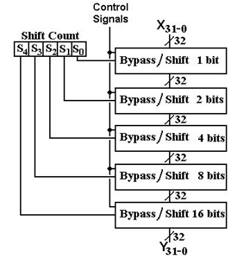
Figure: The Barrel
Shifter
Here are the control signals, listed by instruction. Note that the Shift Count register is hardwired to bits 19 – 15 of the Instruction Register and available for use by the shifter. In the figure above, the 32-bit input to the shift register is indicated by X31-0 and the 32-bit output by Y31-0. We shall discuss the barrel shifter and its connection to the rest of the Arithmetic-Logic unit when we discuss the design of the ALU.
LLS Op-Code = 10000 (Hexadecimal
0x10)
F, T0: PC
®
B1, tra1, B3 ®
MAR, READ. // MAR ¬ (PC)
F, T1: PC ® B1, 1 ® B2, add, B3 ® PC. // PC ¬ (PC) + 1
F, T2: MBR ® B2, tra2, B3 ® IR. // IR ¬
(MBR)
F, T3: R ® B2, shift, ![]() = 1, A = 0. C =
0, B3 ®
R.
= 1, A = 0. C =
0, B3 ®
R.
LCS Op-Code = 10001 (Hexadecimal
0x11)
F, T0: PC
®
B1, tra1, B3 ®
MAR, READ. // MAR ¬ (PC)
F, T1: PC ® B1, 1 ® B2, add, B3 ® PC. // PC ¬ (PC) + 1
F, T2: MBR ® B2, tra2, B3 ® IR. // IR ¬
(MBR)
F, T3: R ® B2, shift, ![]() = 1, A = 0. C =
1, B3 ®
R.
= 1, A = 0. C =
1, B3 ®
R.
RLS Op-Code = 10010 (Hexadecimal
0x12)
F, T0: PC
®
B1, tra1, B3 ®
MAR, READ. // MAR ¬ (PC)
F, T1: PC ® B1, 1 ® B2, add, B3 ® PC. // PC ¬ (PC) + 1
F, T2: MBR ® B2, tra2, B3 ® IR. // IR ¬
(MBR)
F, T3: R ® B2, shift, ![]() = 0, A = 0. C =
0, B3 ®
R.
= 0, A = 0. C =
0, B3 ®
R.
RAS Op-Code = 10011 (Hexadecimal
0x13)
F, T0: PC
®
B1, tra1, B3 ®
MAR, READ. // MAR ¬ (PC)
F, T1: PC ® B1, 1 ® B2, add, B3 ® PC. // PC ¬ (PC) + 1
F, T2: MBR ® B2, tra2, B3 ® IR. // IR ¬
(MBR)
F, T3: R ® B2, shift, ![]() = 0, A = 1. C =
0, B3 ®
R.
= 0, A = 1. C =
0, B3 ®
R.
NOT Op-Code = 10100 (Hexadecimal
0x14)
F, T0: PC
®
B1, tra1, B3 ®
MAR, READ. // MAR ¬ (PC)
F, T1: PC ® B1, 1 ® B2, add, B3 ® PC. // PC ¬ (PC) + 1
F, T2: MBR ® B2, tra2, B3 ® IR. // IR ¬
(MBR)
F, T3: R ® B2, not, B3 ® R.
As noted in above, the negate instruction is syntactic sugar, implemented as subtraction from the constant register %R0 º 0. One has two choices other than implementing both subtract and negate as ALU primitives – either to implement the negate and convert subtraction to adding the negated value (thus A – B = A + ( – B) ), or implement the subtract and have negation as subtraction from 0 (thus – B = 0 – B). This design opts for the latter.
Binary Register-To-Register
These instructions take the contents of two source registers as input
(hence the name “binary”) and copy the result to a destination register. The design allows for the two source
registers to be the same and either or both of the source registers to be the
same as the destination register. Here
are the control signals for these operations.
ADD Op-Code = 10101 (Hexadecimal
0x15)
F, T0: PC
®
B1, tra1, B3 ®
MAR, READ. // MAR ¬ (PC)
F, T1: PC ® B1, 1 ® B2, add, B3 ® PC. // PC ¬ (PC) + 1
F, T2: MBR ® B2, tra2, B3 ® IR. // IR ¬
(MBR)
F, T3: R ® B1, R ® B2, add, B3 ® R.
SUB Op-Code = 10110 (Hexadecimal
0x16)
F, T0: PC
®
B1, tra1, B3 ®
MAR, READ. // MAR ¬ (PC)
F, T1: PC ® B1, 1 ® B2, add, B3 ® PC. // PC ¬ (PC) + 1
F, T2: MBR ® B2, tra2, B3 ® IR. // IR ¬
(MBR)
F, T3: R ® B1, R ® B2, sub, B3 ® R.
AND Op-Code = 10111 (Hexadecimal
0x17)
F, T0: PC
®
B1, tra1, B3 ®
MAR, READ. // MAR ¬ (PC)
F, T1: PC ® B1, 1 ® B2, add, B3 ® PC. // PC ¬ (PC) + 1
F, T2: MBR ® B2, tra2, B3 ® IR. // IR ¬
(MBR)
F, T3: R ® B1, R ® B2, and, B3 ® R.
OR Op-Code = 11000 (Hexadecimal
0x18)
F, T0: PC
®
B1, tra1, B3 ®
MAR, READ. // MAR ¬ (PC)
F, T1: PC ® B1, 1 ® B2, add, B3 ® PC. // PC ¬ (PC) + 1
F, T2: MBR ® B2, tra2, B3 ® IR. // IR ¬
(MBR)
F, T3: R ® B1, R ® B2, or, B3 ® R.
XOR Op-Code = 11001 (Hexadecimal
0x19)
F, T0: PC
®
B1, tra1, B3 ®
MAR, READ. // MAR ¬ (PC)
F, T1: PC ® B1, 1 ® B2, add, B3 ® PC. // PC ¬ (PC) + 1
F, T2: MBR ® B2, tra2, B3 ® IR. // IR ¬
(MBR)
F, T3: R ® B1, R ® B2, xor, B3 ® R.