We now turn to commercial realities, specifically legacy I/O devices. When upgrading a computer, most users do not
want to buy all new I/O devices (expensive) to replace older devices that still
function well. The I/O system must
provide a number of busses of different speeds, addressing capabilities, and
data widths, to accommodate this variety of I/O devices.
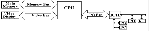
Here we show the main I/O bus connecting the CPU to the I/O Control Hub (ICH), which is
connected to two I/O busses: one for
slower (older) devices
one for faster (newer)
devices.
The requirement to handle memory as
well as a proliferation of I/O devices has lead to a new design based on two
controller hubs:
1. The Memory Controller Hub or “North
Bridge”
2. The I/O Controller Hub or “South
Bridge”
Such a design allows for grouping the higher–data–rate
connections on the faster controller, which is closer to the CPU, and grouping
the slower data connections on the slower controller, which is more removed
from the CPU. The names “Northbridge”
and “Southbridge” come from analogy to the way a map is presented. In almost all chipset descriptions, the
Northbridge is shown above the Southbridge.
In almost all maps, north is “up”.
It is worth note that, in later designs, much of the
functionality of the Northbridge has been moved to the CPU chip.
Backward
Compatibility in System Buses
The early evolution of the Intel microcomputer line provides
an interesting case study in the effect of commercial pressures on system bus
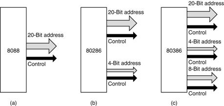
design. We focus on three of the
earliest models, the Intel 8086, Intel 80286, and Intel 80386. All three had 16–bit data lines.
The Intel 8086 had a 20–bit
address line. It could address 1 MB of
memory.
The Intel 80286 had a 24–bit
address line. It could address 16 MB of
memory.
The Intel 80386 had a 32–bit
address line. It could address 4 GB of
memory.
Here is a figure showing the growth of the address bus
structure for these three designs. Note
that an old style (Intel 8086) bus interface card could be inserted into the
20–bit slot of either the Intel 80286 or Intel 80386, and still function
normally. The Intel 80286 interface,
with its 24 bits of address split into two parts, could fit the 24–bit (20 bits
and 4 bits) slot of the Intel 80386.
The Intel 80286 was marketed as the IBM PC/AT (Advanced
Technology). Your author fondly
remembers his PC/AT from about 1986; it was his first computer with a hard disk
(40 MB).
Detour:
The IBM Micro–Channel Bus
The Micro–Channel Architecture was a proprietary bus created
by IBM in the 1980’s for use on their new PS/2 computers. It was first introduced in 1987, but never
became popular. Later, IBM redesigned
most of these systems to use the PCI bus design (more on this later). The PS/2 line was seen by IBM as a follow–on
to their PC/AT line, but was always too costly, typically selling at a
premium. In 1990, the author of this
textbook was authorized to purchase a new 80386–class computer for his
office. The choice was either an IBM MCA
unit or a PC clone. This was put out for bids.
When the bids were received, the lowest IBM price was over $5,000, while
a compatible PC of the same power was $2,900.
According to Wikipedia
“Although MCA was a huge technical improvement over ISA, its introduction
and marketing by IBM was poorly handled. IBM did not develop a peripheral card
market for MCA, as it had done for the PC. It did not offer a number of
peripheral cards that utilized the advanced bus-mastering and I/O processing
capabilities of MCA. Absent a pattern, few peripheral card manufacturers
developed such designs on their own. Consequently customers were not provided
many advanced capabilities to justify the purchase of comparatively more
expensive MCA systems and opted for the plurality of cheaper ISA designs
offered by IBM's competition.”
“IBM had patents on MCA system features and required MCA system
manufacturers to pay a license fee. As a reaction to this, in late 1988 the
"Gang of Nine", led by Compaq, announced a rival bus – EISA. Offering
similar performance benefits, it had the advantage of being able to accept
older XT and ISA boards.”
“MCA also suffered for being a proprietary technology. Unlike their
previous PC bus design, the AT bus, IBM did not publicly release specifications
for MCA and actively pursued patents to block third parties from selling
unlicensed implementations of it, and the developing PC clone market did not
want to pay royalties to IBM in order to use this new technology. The PC clone
makers instead developed EISA as an extension to the existing old AT bus
standard. The 16–bit AT bus was embraced and renamed as ISA to avoid IBM's
"AT" trademark. With few vendors other than IBM supporting it with
computers or cards, MCA eventually failed in the marketplace.”
“While EISA and MCA battled it out in the server arena, the desktop PC
largely stayed with ISA up until the arrival of PCI, although the VESA Local
Bus, an acknowledged stopgap, was briefly popular.” [R92]
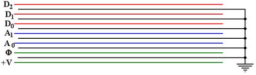
Notations
Used for a Bus
We pause here in our historical discussion of bus design to
introduce a few terms used to characterize these busses. We begin with some conventions used to draw
busses and their timing diagrams. Here
is the way that we might represent a bus with multiple types of lines.
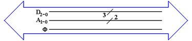
The big “double arrow” notation indicates a bus of a number
of different signals. Some authors call
this a “fat arrow”. Lines with similar
function are grouped together. Their
count is denoted with the “diagonal slash” notation. From top to bottom, we have
1. Three data lines D2,
D1, and D0
2. Two address lines A1
and A0
3. The clock signal for the bus F.
Not all busses
transmit a clock signal; the system bus usually does.
Power and ground lines usually are not shown in this type of
diagram. Note the a bus with only one
type of signal might be drawn as a thick line with the slash, as in the 3 – bit
data bus above.
Maximum Bus Length
In general, bus length varies inversely as transmission
speed, often measured in Hz; e.g., a
1 MHz bus can make one million transfers per second and a 2 GHz bus can make
two billion.
Immediately we should note that the above is not exactly true of DDR (Double
Data Rate) busses which transfer at twice the bus speed; a 500 MHz DDR bus
transfers 1 billion times a second.
Note that the speed in bytes per second is related to the number of bytes per
transfer. A DDR bus rated at 400 MHz and
having 32 data lines would transfer 4 bytes 800 million times a second, for a
total of 3.20 billion bytes per second.
Note that this is the peak transfer rate.
The relation of the bus speed to bus length is due to signal
propagation time. The speed of light is
approximately 30 centimeters per nanosecond.
Electrical signals on a bus typically travel at
2/3 the speed of light; 20 centimeters per nanosecond or 20 meters per
microsecond.
A loose rule of thumb in sizing busses is that the signal
should be able to propagate the entire length of the bus twice during one clock
period. Thus, a 1 MHz signal would have
a one microsecond clock period, during which time the signal could propagate no
more than twenty meters. This length is
a round trip on a ten meter bus; hence, the maximum length is 10 meters. Similarly, a 1 GHz signal would lead to a
maximum bus length of ten centimeters.
The rule above is only a rough estimator, and may be
incorrect in some details. Since the
typical bus lengths on a modern CPU die are on the order of one centimeter or
less, we have no trouble.
Bus Classifications
It should be no surprise that, depending on the feature
being considered, there are numerous ways to characterize busses. We have already seen one classification, what
might be called a “mixed bus” vs. a “pure bus”; i.e., does the bus carry more
than one type of signal. Most busses are
of the mixed variety, carrying data, address, and control signals. The internal CPU busses on our design carry
only data because they are externally controlled by the CPU Control Unit that
sends signals directly to the bus end points.
One taxonomy of busses refers to
them as either point–to–point vs. shared.
Here is a picture of that way of looking at busses.
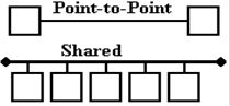
An example of a point–to–point
bus might be found in the chapter on computer internal memory, where we
postulated a bus between the MBR and the actual memory chip set. Most commonly, we find shared busses with a number of devices attached.
Another way of characterizing busses is by the number of
“bus masters” allowed. A bus master is a device that has
circuitry to issue command signals and place addresses on the bus. This is in distinction to a “bus slave” (politically incorrect
terminology) that can only transfer data in response to commands issued by a
bus master. In the early designs, only
the CPU could serve as a bus master for the memory bus. More modern memory busses allow some
input/output devices (discussed later as DMA devices) to act as bus masters and
transfer data to the memory.
Bus Clocks
Another way to characterize busses is whether the bus is
asynchronous or synchronous. A synchronous bus is one that has one or
more clock signals associated with it, and transmitted on dedicated clock
lines. In a synchronous bus, the signal
assertions and data transfers are coordinated with the clock signal, and can be
said to occur at predictable times.
An asynchronous
bus is one without a clock signal. The
data transfers and some control signal assertions on such a bus are controlled
by other control signals. Such a bus
might be used to connect an I/O unit with unpredictable timing to the CPU. The I/O unit might assert some sort of ready signal when it can undertake a
transfer and a done signal when the
transfer is complete.
In order to understand these busses more fully, it would
help if we moved on to a discussion of the bus timing diagrams and signal
levels.
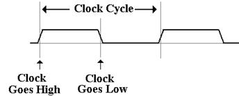
Bus Signal Levels
Many times bus operation is illustrated with a timing
diagram that shows the value of the digital signals as a function of time. Each signal has only two values,
corresponding to logic 0 and to logic 1.
The actual voltages used for these signals will vary depending on the
technology used.
A bus signal is
represented in some sort of trapezoidal form with rising edges and falling
edges, neither of which is represented as a vertical line. This convention emphasizes that the signal
cannot change instantaneously, but takes some time to move between logic high
and low. Here is a depiction of the bus
clock, represented as a trapezoidal wave.
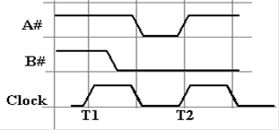
Here is a sample
diagram, showing two hypothetical discrete signals. Here the discrete signal B# goes low during
the high phase of clock T1 and stays low.
Signal A# goes low along with the second half of clock T1 and stays low
for one half clock period.
A collection of
signals, such as 32 address lines or 16 data lines cannot be represented with
such a simple diagram. For each of
address and data, we have two important states; the signals are valid, and
signals are not valid
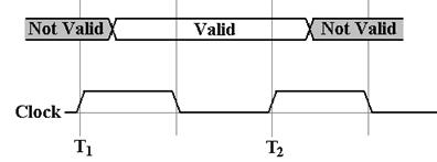
For example,
consider the address lines on the bus.
Imagine a 32–bit address. At some
time after T1, the CPU asserts an address on the address lines. This means that each of the 32 address lines
is given a value, and the address is valid until the middle of the high part of
clock pulse T2, at which the CPU ceases assertion.
Having seen these conventions, it is time to study a pair of
typical timing diagrams. We first study
the timing diagram for a synchronous bus.
Here is a read timing diagram.
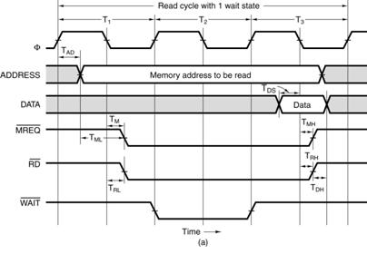
What we have here is a timing diagram that covers three full
clock cycles on the bus. Note that
during the high clock phase of T1, the address is asserted on the
bus and kept there until the low clock phase of T3. Before and after these times, the contents of
the address bus are not specified. Note
that this diagram specifies some timing constraints. The first is TAD, the maximum
allowed delay for asserting the address after the clock pulse if the memory is
to be read during the high phase of the third clock pulse.
Note that the memory chip will assert the data for one half
clock pulse, beginning in the middle of the high phase of T3. It is during that time that the data are
copied into the MBR.
Note that the three control signals of interest (  ) are asserted low. We also have another constraint TML,
the minimum time that the address is stable before the
) are asserted low. We also have another constraint TML,
the minimum time that the address is stable before the  is asserted.
The purpose of the diagram above is to indicate what has to
happen and when it has to happen in order for a memory read to be successful
via this synchronous bus. We have four
discrete signals (the clock and the three control signals) as well as two
multi–bit values (memory address and data).
For the discrete signals, we are interested in the specific
value of each at any given time. For the
multi–bit values, such as the memory address, we are only interested in
characterizing the time interval during which the values are validly asserted
on the data lines.
Note that the more modern terminology for the three control
signals that are asserted low would be MREQ#,
RD#, and WAIT#.
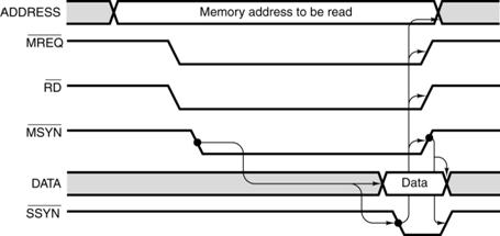
The timing diagram for an asynchronous bus includes some
additional information. Here the focus
is on the protocol by which the two devices interact. This is also called the “handshake”. The bus master asserts MSYN# and the bus
slave responds with SSYN# when done.
The asynchronous bus uses similar notation for both the
discrete control signals and the
multi–bit values, such as the address and data.
What is different here is the “causal arrows”, indicating that the
change in one signal is the causation of some other event. Note that the assertion of MSYN# causes the memory chip to place
data on the bus and assert SSYN#. That assertion causes MSYN# to be dropped, data to be no longer asserted, and then SSYN# to drop.
Multiplexed
Busses
A bus may be either multiplexed or non–multiplexed. In a multiplexed
bus, bus data and address share the same lines, with a control signal to
distinguish the use. A non–multiplexed bus has separate lines
for address and data. The multiplexed
bus is cheaper to build in that it has fewer signal lines. A non–multiplexed bus is likely faster.
There is a variant of multiplexing, possibly called “address multiplexing” that is seen on
most modern memory busses. In this
approach, an N–bit address is split into two (N/2)–bit addresses, one a row
address and one a column address. The
addresses are sent separately over a dedicated address bus, with the control
signals specifying which address is being sent.
Recall that most modern memory chips are designed for such
addressing. The strategy is to specify a
row, and then to send multiple column addresses for references in that
row. Some modern chips transmit in burst
mode, essentially sending an entire row automatically.
Here, for reference, is the control signal description from
the chapter on internal memory.
|
CS#
|
RAS#
|
CAS#
|
WE#
|
Command / Action
|
|
1
|
d
|
d
|
d
|
Deselect
/ Continue previous operation
|
|
0
|
1
|
1
|
1
|
NOP
/ Continue previous operation
|
|
0
|
0
|
1
|
1
|
Select
and activate row
|
|
0
|
1
|
0
|
1
|
Select
column and start READ burst
|
|
0
|
1
|
0
|
0
|
Select
column and start WRITE burst
|
More
on Real Bus Architecture
Here we offer some information on a now–obsolete bus of some
historical interest. For those that are
not interested in the history, we note that this presents a chance to discuss
some issues related to bus design that have not yet been broached.
The bus in question is the PDP–11 Unibus™, manufactured in
the 1970’s by the Digital Equipment Corporation. We first discuss the use of ground
lines. Ground lines on the bus have two
purposes
1. to complete the electrical circuits, and
2. to minimize cross–talk between the signal lines.
Cross–talk occurs when a signal on
one bus line radiates to and is copied by another bus line. Placing a ground line between 2 lines
minimizes this. This small bus is
modeled on the Unibus.
The variety of signals that can be placed on a bus is seen
in the following table adapted from the PDP-11 Peripherals Handbook [R3]. Note that this bus operates as an
asynchronous bus, which will allow slower I/O devices to use the bus.
|
Name
|
Mnemonic
|
Lines
|
Function
|
Asserted
|
|
TRANSFER LINES
|
|
|
|
|
|
Address
|
A<17:00>
|
18
|
Selects device or memory
|
Low
|
|
Data
|
D<15:00>
|
16
|
Data for transfer
|
Low
|
|
Control
|
C0, C1
|
2
|
Type of data transfer
|
Low
|
|
Master Sync
|
MSYN
|
1
|
Timing controls for data transfer
|
Low
|
|
Slave Sync
|
SSYN
|
1
|
Low
|
|
Parity
|
PA, PB
|
2
|
Device parity error
|
Low
|
|
Interrupt
|
INTR
|
1
|
Device interrupt
|
Low
|
|
PRIORITY LINES
|
|
|
|
|
|
Bus Request
|
BR4, BR5, BR6, BR7
|
4
|
Requests use of bus
|
Low
|
|
Bus Grant
|
BG4, BG5, BG6, BG7
|
4
|
Grants use of bus
|
High
|
|
Selection Acknowledge
|
SACK
|
1
|
Acknowledges grant
|
Low
|
|
Bus Busy
|
BBSY
|
1
|
Data section in use
|
Low
|
|
INITIALIZATION
|
|
|
|
|
|
Initialize
|
INIT
|
1
|
System Reset
|
Low
|
|
AC Low
|
AC LO
|
1
|
Monitor power
|
Low
|
|
DC Low
|
DC LO
|
1
|
Monitor power
|
Low
|
Figure: PDP-11 UNIBUS CONTROL
SIGNALS
We see
above the expected data and address lines, though noting the small address
size. We see most of the expected
control lines (MSYN# and SSYN#). What
about the priority lines? These are control
lines that allow an I/O device to signal the CPU that it is ready to transfer
data.
The Boz
series of computer designs follows the PDP–11 model in that it has four
priority levels for I/O devices. While
this strategy will be discussed more fully in a future chapter, we note here
that the bus used for the I/O devices to communicate with the CPU must have two
lines for each level in order for the interrupt structure to function.
The above figure suggests that the PDP–11 can operate in one
of eight distinct priority levels, from 0 to 7.
The upper four levels (4, 5, 6, and 7) are reserved for handling I/O
devices. The lower four levels (0, 1, 2,
and 3) were probably never fully implemented.
Normal programs run at priority 0, and the other three levels (1, 2, and
3) are probably ignored. At each level,
the bus provides two lines: BR (bus request) that is the interrupt line, and BG
(bus grant) that signals the device to start transferring data. As indicated above, we shall say more on this
very soon.
Modern
Computer Busses
The next major step in evolution of the computer bus took
place in 1992, with the introduction by Intel of the PCI (Peripheral Component
Interconnect) bus. By 1995, the bus was
operating at 66 MHz, and supporting both a 32–bit and 64–bit address space.
According to Abbott [R64], “PCI evolved, at least in part,
as a response to the shortcomings of the then venerable ISA bus. … ISA began to run out of steam in 1992, when
Windows had become firmly established.”
Revision 1 of the PCI standard was published in April 1993.
The PCI bus standard has evolved into the PCI Express
standard, which we shall now discuss.
PCI
Express
PCI Express
(Peripheral Component Interconnect Express) is a computer expansion card
standard designed to replace the older PCI bus standard. The name is abbreviated as “PCIe”. This is viewed as a standard for computer
expansion cards, but really is a standard for the communication link by which a
compliant device will communicate over the bus.
According to
Wikipedia [R93], PCIe 3.0 (August 2007) is the latest standard. While an outgrowth of the original PCI bus
standard, the PCIe is not compatible with that standard at the hardware
level. The PCIe standard is based on a
new protocol for electrical signaling.
This protocol is built on the concept of a lane, which we must define. A PCI connection can comprise from 1 to 32
lanes. Here are some capacity quotes
from Wikipedia
Per
Lane 16–Lane
Slot
Version 1 250
MB/s 4 GB/s
Version 2 500
MB/s 8 GB/s
Version 3 1
GB/s 16
GB/s
What
is a Lane?
A
lane is pair of point–to–point serial links, in other words the lane is a
full–duplex link, able to communicate in two directions simultaneously. Each of the serial links in the pair handles
one of the two directions.
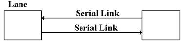
By definition, a
serial link transmits one bit at a
time. By extension, a lane may transmit two bits at any one
time, one bit in each direction. One may
view a parallel link, transmitting multiple
bits in one direction at any given time, as a collection of serial links. The only difference is that a parallel link
must provide for synchronization of the bits sent by the individual links.
Data
Transmission Codes
The PCIe
standard is byte oriented, in that it should be viewed logically as a
full–duplex byte stream. What is
actually transmitted? The association of
bits (transmitted or received) with bytes is handled at the Data Link
layer. Suppose a byte is to be
transmitted serially.
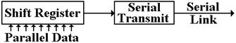
The conversion
from byte data to bit–oriented data for serial transmission is done by a shift
register. The register takes in eight
bits at a time and shifts out one bit at a time. The bits, as shifted out, are still
represented in standard logic levels. The
serial transmit unit takes the standard logic levels as input, and converts
them to voltage levels appropriate for serial transmission.
Three
Possible Transmission Codes
The serial
transmit unit sends data by asserting a voltage on the serial link. The simplest method would be as follows.
To transmit a logic 1, assert
+5 volts on the transmission line.
To transmit a logic 0, assert
0 volts on the transmission line.
There are very
many problems with this protocol. It is
not used in practice for any purpose other than transmitting power. The two main difficulties are as
follows. The first problem is that of
transmitting power. If the average
voltage (over time) asserted by a transmitter on a line is not zero, then the
transmitter is sending power to the receiver.
This is not desirable. The answer
to this is to develop a protocol such that the time–averaged voltage on the
line is zero. Such a protocol might call
for enough changes in the voltage level to allow for data framing. Standard methods for link management use codes
that avoid these problems. Two of the
more common methods used are NRZ and NRZI.
Non–Return–to–Zero coding transmits by asserting
the following voltages:
For a logic 1, it asserts a
positive voltage (3.0 – 5.0 volts) on the link.
For a logic 0, it asserts a
negative voltage (–3.0 to –5.0 volts).
Non–Return–to–Zero–Invert is a
modification of NRZ, using the same
voltage levels.
The
Problem of Noise
One problem with
these serial links is that they function as antennas. They will pick up any stray electromagnetic
radiation if in the radio range.
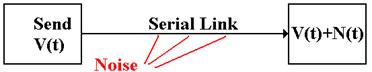
In other words,
the signal received at the destination might not be what was actually
transmitted. It might be the original
signal, corrupted by noise. The solution
to the problem of noise is based on the observation that two links placed in
close proximity will receive noise signals that are almost identical. To make use of this observation, we use differential transmitters [ R94] to send the signals and differential receivers to reconstruct
the signals.
In differential
transmission, rather than asserting a voltage on a single output line, the
transmitter asserts two voltages: +V/2 and –V/2. A +6 volt signal would be asserted as two: +3
volts and –3 volts. A –8 volt signal
would be asserted as two: –4 volts and +4 volts.
Here are the
standard figures for a differential transmitter and differential receiver. The standard receiver is an analog subtractor,
here giving V/2 – (–V/2) = V.
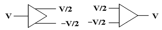
Differential
Transmitter Differential
Receiver
Noise
in a Differential Link
We now assume
that the lines used to transmit the differential signals are physically close
together, so that each line is subject to the same noise signal.
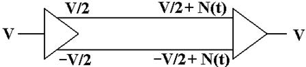
Here the
received signal is the difference of the two voltages input to the differential
receiver. The value received is ( V/2 +N(t) ) – ( –V/2 + N(t) ) = V, the
desired value.
Ground
Offsets in Standard Links
All voltages are
measured relative to a standard value, called “ground”. Here is the
complete version of the simple circuit that we want to implement.
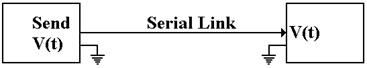
Basically, there
is an assumed second connection between the two devices. This second connection fixes the zero level
for the voltage.
There is no
necessity for the two devices to have the same ground. Suppose that the ground for the receiver is
offset from the ground of the transmitter.
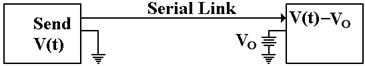
The signal sent
out as +V(t) will be received as V(t) – VO. Here again, the subtractor in the
differential receiver handles this problem.
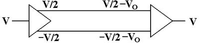
The signal
originates as a given voltage, which can be positive, negative, or 0. The signal is transmitted as the pair (+V/2,
–V/2). Due to the ground offset, the
signal is taken in as
(+V/2 – VO, –V/2 – VO), interpreted as (+V/2 – VO)
– (–V/2 – VO) = +V/2 – VO + V/2 + VO = V.
The differential
link will correct for both ground offset and line noise at the same time.
Note: The author of this text became interested in the PCIe bus standard
after reading product descriptions for the NVIDIA C2070 Computing Processor
(www.nvidia.com). This is a very high
performance coprocessor that attaches to the host via a 16–lane PCIe bus. What is such a bus? What is a lane? Professors want to know.
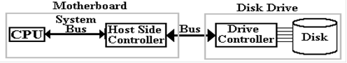
Interfaces
to Disk Drives
The disk drive
is not a stand–alone device. In order to
function as a part of a system, the disk must be connected to the motherboard
through a bus. We shall discuss details
of disk drives in the next chapter. In
this one, we focus on two popular bus technologies used to interface a disk:
ATA and SATA. Much of this material is
based on discussions in chapter 20 of the book on memory systems by Bruce
Jacob, et al [R99].
The top–level
organization is shown in the figure below.
We are considering the type of bus used to connect the disk drive to the
motherboard; more specifically, the host controller on the motherboard to the
drive controller on the disk drive. While
the figure suggests that the disk is part of the disk drive, this figure
applies to removable disks as well. The
important feature is the nature of the two controllers and the protocol for
communication between them.
One of the
primary considerations when designing a disk interface, and the bus to
implement that interface, is the size of the drive controller that is packaged
with the disk. As Jacob [R99] put it:
“In the early
days, before Large Scale Integration (LSI) mad adequate computational power
economical to be put in a disk drive, the disk drives were ‘dumb’ peripheral
devices. The host system had to
micromanage every low–level action of the disk drive. … The host system had to
know the detailed physical geometry of the disk drive; e.g., number of
cylinders, number of heads, number of sectors per track, etc.”
“Two things
changed this picture. First, with the
emergence of PCs, which eventually became ubiquitous, and the low–cost disk
drives that went into them, interfaces became standardized. Second, large–scale integration technology in
electronics made it economical to put a lot of intelligence in the disk side
controller”
As of Summer
2011, the four most popular interfaces (bus types) were the two varieties of
ATA (Advanced Technology Attachment, SCSI (Small Computer Systems Interface0,
and the FC (Fibre Channel). The SCSI and
FC interfaces are more costly, and are commonly used on more expensive
computers where reliability is a premium.
We here discuss the two ATA busses.
The ATA
interface is now managed by Technical Committee 13 of INCITS (www.t13.org), the
International Committee for Information Technology Standards (www.incits.org). The interface was so named because it was
designed to be attached to the IBM PC/AT, the “Advanced Technology” version of
the IBM PC, introduced in 1984. To quote
Jacob again:
“The first hard
disk drive to be attached to a PC was Seagate’s ST506, a 5.25 inch form factor
5–MB drive introduced in 1980. The drive
itself had little on–board control electronics; most of the drive logic resided
in the host side controller. Around the
second half of the 1980’s, drive manufacturers started to move the control
logic from the host side and integrate it with the drive. Such drives became known as IDE (Integrated
Drive Electronics) drives.”
In recent years,
the ATA standard has being explicitly referred to at the “PATA” (Parallel ATA)
standard to distinguish it from the SATA (Serial ATA standard) that is now
becoming popular. The original PATA
standard called for a 40–wire cable. As
the bus clock rate increased, noise from crosstalk between the unshielded
cables became a nuisance. The new design
included 40 extra wires, all ground wires to reduce the crosstalk.
As an example of
a parallel bus, we show a picture of the PDP–11 Unibus. This had 72 wires, of which 56 were devoted
to signals, and 16 to grounding. This
bus is about 1 meter in length.
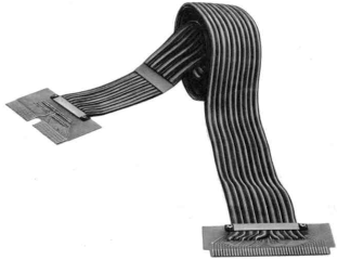
Figure: The
Unibus of the PDP–11 Computer
Up to this
point, we have discussed parallel busses.
These are busses that transmit N data bits over N data lines, such as
the Unibus™ that used 16 data lines to transmit two bytes per transfer. Recently serial busses have become popular;
especially the SATA (Serial Advanced Technology Attachment) busses used to
connect internally mounted disk drives to the motherboard. There are two primary motivations for the
development of the SATA standard: clock skews and noise.
The problem of
clock skew is illustrated by the following pair of figures. The first figure shows a part of the timing
diagram for the intended operation of the bus.
While these figures may be said to be inspired by actual timing
diagrams, they are probably not realistic.
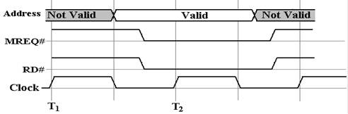
In the above figure, the control signals MREQ# and RD# are
asserted simultaneously one half clock time, after the address becomes
valid. The two are simultaneously
asserted for two clock times, after which the data are read.
We now imagine what could go wrong when the clock time is
very close to the gate delay times found in the circuitry that generates these
control signals. For example, let us
assume a 1 GHz bus clock with a clock time of one nanosecond. The timing diagram above calls for the two
control signals, MREQ# and RD#, to be asserted 0.5 nanoseconds (500
picoseconds) after the address is valid.
Suppose that the circuit for each of these is skewed by 0.5 nanoseconds,
with the MREQ# being early and the RD# being late.
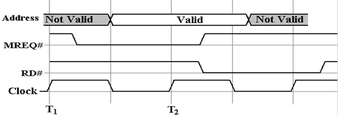
What we have in this diagram is a mess, one that probably
will not lead to a functional read operation.
Note that MREQ# and RD# are simultaneously asserted for only an instant,
far too short a time to allow any operation to be started. The MREQ# being early may or may not be a
problem, but the RD# being late certainly is.
A bus with these skews will not work.
As discussed above, the ribbon cable of the PATA bus has 40
unshielded wires. These are susceptible
to cross talk, which limits the permissible clock rate. What happens is that crosstalk is a transient
phenomenon; the bus must be slow enough to allow its effects to dissipate.
We have already seen a solution to the problem of noise when
we considered the PCI Express bus. This
is the solution adopted by the SATA bus.
The standard SATA bus has a seven–wire cable for signals and a separate
five–wire cable for power. The
seven–wire cable for data has three wires devoted to ground (noise reduction)
and four wires devoted to a serial lane, as described above for PCI
Express. As noted above in that
discussion, the serial lane is relatively immune to noise and crosstalk, while
allowing for very good transmission speeds.
One might note that parallel busses are inherently faster
than serial busses. An N–bit bus will
transmit data N times faster than a 1–bit serial bus. The experience seems to be that the data
transmission rate can be so much higher on the SATA bus than on a parallel bus,
that the SATA bus is, in fact, the faster of the two. Data transmission on these busses is rated in
bits per second. In 2007, according to
Jacob [R99] “SATA controllers and disk drives with 3 Gbps are starting to
appear, with 6 Gbps on SATA’s roadmap.”
The encoding used is called “8b/10b”, in which an
8–bit byte is padded with two error correcting bits to be transmitted as 10
bits. The two speeds above correspond to
300 MB per second and 600 MB per second.