Chapter 9
Appendix – Interfacing the CPU to SDRAM
In this chapter,
we consider the interface between the Boz–7 CPU and the more modern memory
technology that we have postulated in the previous chapter. There are two reasons for this chapter. The primary reason is to illustrate the
nature of such an interface. Another
reason is that your author is too lazy to change the design of the CPU control
unit to be compatible with the more modern memory designs, so he must provide
an interface.
There
are two parts to this interface.
1. The
interface for the memory control signals, especially the generation of the
memory address and control
signals. In the more modern terminology,
the
control signals are CAS#
and RAS# (Column Address Select and Row Address
Select, each active low).
2. The
design of the MBR (Memory Buffer Register) as an interface between the
internal CPU busses and the
memory bus.
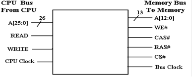
The
original Boz series of computers was designed to accommodate 64 M 32–bit
words. That is
226 words, each of 32 bits.
Another way to put this is that the memory has size 256 MB. The memory is addressed with a 26–bit address
A[25:0].
The
memory is controlled by two signals, both active high, according to the
following table. Note that READ = 1 and
WRITE = 1 would seem to indicate that the memory is to be read and written at
the same time. Only one option at a time
is allowed; the tie was broken arbitrarily.
|
READ |
WRITE |
Action |
|
0 |
0 |
Nothing happens |
|
0 |
1 |
CPU writes to memory |
|
1 |
0 |
CPU reads from memory, an arbitrary choice. |
|
1 |
1 |
This diagram
represents the address interface problem.
It will be revised later in the chapter.
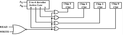
Immediately,
we can derive equations for WE# and CS#, assuming that there is only one
chip. In actual fact there will be more
than one memory chip, but the CS# developed here will be an input to the values
sent to each of the multiple chips.
|
READ |
WRITE |
CS# |
WE# |
|
0 |
0 |
1 |
d |
|
0 |
1 |
0 |
0 |
|
1 |
0 |
0 |
1 |
|
1 |
1 |
0 |
1 |
Given
the fact that WE# is not used when CS# = 1, we have the following equations.
![]()
Note
that WE# = 0 when READ = 0 and WRITE = 0.
In that case CS# = 1, so none of the memory chips are active. If multiple memory banks are used, then the
signal CS# is modified. Here is the
circuit as it would appear were we to use 4–way low–order interleaved memory.
The
next step is to devise a circuit that produces the memory bus clock from the
CPU clock. Just to
show that powers of two are not sacrosanct, we show a divide–by–three circuit.
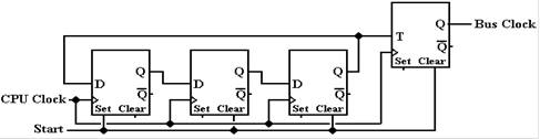
This
is a one–hot modulo–3 counter. On every
third pulse, the input to the T flip–flop is set to 1 and that flip–flop
toggles. The bus clock output from the T
has frequency 1/3 of the CPU clock. All
that is generally true is the CPU clock frequency is some integer multiple of
the bus clock frequency, as the bus clock is derived from the CPU clock by
methods similar to that above.
The
next step is to derive RAS# and CAS# from the bus clock. The memory for our design will be controlled
in a manner similar to the MT47H128M16 discussed in the previous chapter.
|
CS# |
RAS# |
CAS# |
WE# |
Command / Action |
|
1 |
d |
d |
d |
Deselect
/ Continue previous operation |
|
0 |
1 |
1 |
1 |
NOP
/ Continue previous operation |
|
0 |
0 |
1 |
1 |
Select
and activate row |
|
0 |
1 |
0 |
1 |
Select
column and start READ burst |
|
0 |
1 |
0 |
0 |
Select
column and start WRITE burst |
When CS# = 1,
neither RAS# nor CAS# is important. When
CS# = 0, each of RAS# and
CAS# will be driven by the memory bus, as follows.
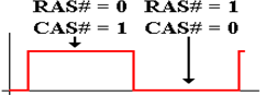
This
suggests the following truth table for determining RAS# and CAS#.
|
CS# |
Bus Clock |
RAS# |
CAS# |
|
1 |
d |
d |
d |
|
0 |
0 |
1 |
0 |
|
0 |
1 |
0 |
1 |
The more robust
set of equations for RAS# and CAS# are as follows.
![]()
We
now consider the circuitry for delivering the address to the memory chip. This is based on the use of a number of
two–to–one multiplexers that are enabled low.
Just for reference, here is a diagram of such a device as it might be
fabricated from basic gates.
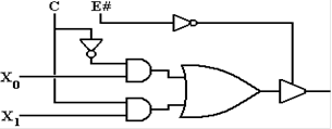
When
E# = 0, the output of the multiplexer depends on the value of the control
signal, C. When
E# = 1, the OR gate of the multiplexer is disconnected from the output.
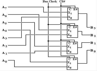
The
following table illustrates the output of this circuit when CS# = 0.
|
Bus Clock |
B3 |
B2 |
B1 |
B0 |
Comment |
|
0 |
A3 |
A2 |
A1 |
A0 |
Column Address |
|
1 |
A7 |
A6 |
A4 |
A4 |
Row Address |
The
next circuit to design is one that allows the Memory Buffer Register (MBR) to
be interfaced to both the internal CPU busses and the memory bus. The CPU design, discussed in a later chapter,
calls for the MBR to take data from CPU bus B3 and place data onto CPU bus B2.
Here
are the two interface scenarios for the MBR, illustrated for a single bit. In the Boz series of computers, the MBR has
32 bits. It transfers a 32–bit word each
time. The function of the MBR is, as its
name suggests, to serve as a buffer between the CPU
and the memory bus. On a CPU write to
memory, the buffer holds data written by the CPU for transfer to the memory
system. On a CPU read from memory, the
buffer holds data taken from memory until the CPU can transfer the data to a
register. The main issue in the data
buffering is the timing difference between the CPU clock and the memory bus
clock.
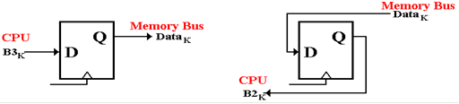
CPU
Writes Data to Memory CPU
Reads Data from Memory
The
solution to this design problem is called a transceiver. Here is one implementation.
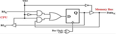
First
consider the connection of the output of the flip–flop in the MBR.
When WE# = 0, the output is
connected to the data line in the memory bus.
When WE# = 1, the output is
connected to the bit line in the CPU bus B2.
Now
consider how the flip–flop is loaded. It
is a negative edge–triggered device, which loads on the falling edge of the
clock input to the flip–flop.
When WE# = 0, the input of the flip–flop is connected to CPU bus B3.
When WE# = 1, the input of the flip–flop is connected to the memory bus,
which is
disconnected from the output of the flip–flop.
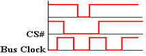 The diagram at
left shows the timing of the control signals.
The signal CS# is asserted as 0 some time during the high phase of the
bus clock and remains low until some time in the next high phase. The clock signal to the flip–flop has a well
defined negative edge, allowing it to be loaded properly.
The diagram at
left shows the timing of the control signals.
The signal CS# is asserted as 0 some time during the high phase of the
bus clock and remains low until some time in the next high phase. The clock signal to the flip–flop has a well
defined negative edge, allowing it to be loaded properly.
Putting It All
Together
At
this time, your author has too many questions about the design to
continue. The main question relates to
how to interleave DDR2 memory chips that transmit in burst mode.