For this course it suffices to note that we must have digital devices with memory and to investigate the most common ways of providing such memory. In electrical engineering terms, memory is a feedback mechanism, in which the output of a combinational circuit is delayed for some amount of time and then fed back as input to the circuit.
The concept of feedback is helpful
to the small number of us with background in an engineering discipline, but
most of us will prefer to think of memory as “bit boxes”
– storage containers that hold one bit of binary information. These bit boxes, called
“flip-flops”, were discussed in the previous chapter.
Before discussing memory devices, let’s review the difference between combinational circuits and sequential circuits.
Combinational Circuits Sequential Circuits
No Memory Memory
No flip-flops, Flip-flops
may be used
only combinational gates Combinational gates may be used
No feedback Feedback is allowed
Output for a given set of The order of input change
Inputs is independent of is
quite important and may
order in which these inputs produce significant
differences
were changed, after the in the output.
output stabilizes.
The following figure shows a way to consider sequential circuits.
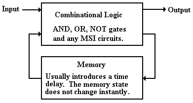
Figure: Sequential Logic Includes
Combinational Logic and Memory
Sequential circuits can be characterized into two broad classes – synchronous and asynchronous. As a general rule, asynchronous circuits are faster, but much harder to design. We shall focus totally on synchronous circuits.
By Q(T) we denote the state of a sequential circuit at time T – this is basically its memory. We watch the state of the circuit change from Q(T) to Q(T + 1) as the clock ticks. The constraint on synchronous circuits is that the state of the circuit changes after the input, thus we have a typical sequence as follows:
1) At time T, we have input (denoted by X)
and state Q(T).
2) As a result of the input X and state Q(T), a new state is
computed,
This becomes
available to the input only at time (T + 1) and so
is called Q(T +
1).
The fact that the new state, computed as a result of X and Q(T), is not available to the input of the sequential circuit until the next time step greatly facilitates the design and analysis of the specific circuit. We do not have endless feedback loops to worry about.
We shall consider two
approaches to understanding sequential circuits:
1) Analysis
of sequential circuits
2) Design
(synthesis) of sequential circuits
Circuit analysis begins with a circuit diagram or a black box and ends with an identification of the sequential circuit implemented by the device – normally a truth table. The steps are:
1) Identify the inputs
and the outputs
2) Express
each output as a Boolean function of the inputs and the present state Q(T)
3) Identify
the circuit if possible.
Circuit design begins with a complete description of the circuit and ends with a design.
Introduction to
Strictly speaking a finite state machine (FSM) is a device that can exist in one of a finite number of states. Associated with an FSM is a memory that is used to store an identifier of the state, so that the machine may process its input (if any) and move to the next state. Due to this coincidence, finite state machines are often studied in conjunction with flip-flops.
We are all familiar with finite state machines, although we rarely think of them as such. Consider a washing machine. The states for this machine are: off, fill with water, wash, spin, and rinse. The control unit for the FSM is the knob on the washer that we turn to start it.
A traffic light is also a finite state machine. We normally think of a traffic light as having only three states: Green, Yellow, and Red. The truth is a bit more complex, in that the physical unit must display at least two sets of lights, one for each intersecting street. Nevertheless, a standard traffic light can be modeled with no more than eight states, although the introduction of advanced green lights and turn signals complicates things a bit.
A standard digital clock that displays only hour, minute,
and second, can be said to have
24 ·
60 ·
60 = 86,400 states – still a finite number.
Normally the FSM construct is used to model systems with far fewer
states; in our work we shall normally limit a FSM to either eight or sixteen
states; that is N £
23 or N £
24.
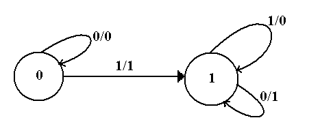
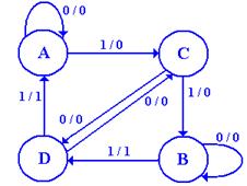
If a finite state machine does not have too many states, we may represent its operation by a state diagram. The following is a state diagram for a circuit called a sequence detector. For those who are interested, this is the state diagram for a 11011 sequence detector; it has five states because it is detecting a five-bit sequence.
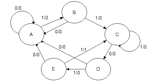
Figure: State Diagram for a 11011 Sequence Detector
At this stage of the presentation, we focus not on the details of generating the state diagram, but just use it as an example of a generic state diagram. What do we note about this one?
1. In terms of
discrete mathematics, it is a directed graph with loops. Thus, it is not
a simple graph. In simple graphs, arcs do not connect any
vertex with itself.
2. The arcs each have
direction and a label of the form X/Z.
What we see here is the
FSM reacting to input by
moving between states and producing output.
In the
X/Z labeling scheme, X is
the binary input (0 or 1) and Z is the binary output.
3. There is output
associated with the transitions. Not all
FSM have output
associated with the
transitions between states. This one
does.
4. This and all
typical FSM represents a synchronous machine; transitions between
states and production of
output (if any) takes place at a fixed phase of the clock,
depending on the
flip-flops used to implement the circuit.
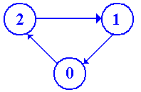
Not all finite state machines have such complex state diagrams.
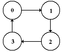 The
figure at left is the state diagram for a modulo-4
The
figure at left is the state diagram for a modulo-4
up-counter. It just counts 0, 1, 2, 3 and
repeats, continually counting up (modulo 4).
There is no input (other than the clock, which we almost never mention)
and no output directly associated with the transitions. For this type of FSM, the output is
associated with the states and not with the transitions.
Figure: State Diagram
for a Modulo-4 Up-Counter
Many mathematical models of FSM focus on the state diagram. For most of our work, it is more convenient to work with the state table of the FSM, a tabular representation of the state diagram. Translation between the state diagram and state table is automatic. The state table presents the data in terms of present state Q(t) and next state Q(t+1) using the labeling that most naturally fits the problem. Here are the state tables for the two FSM above. Note that eh state table contains exactly the same information as the state diagram.
|
|
|
|
|
|
X = 0 |
X = 1 |
|
A |
A / 0 |
B / 0 |
|
B |
A / 0 |
C / 0 |
|
C |
D / 0 |
C / 0 |
|
D |
A / 0 |
E / 0 |
|
E |
A / 0 |
C / 1 |
Figure: State Table for 11011 Sequence Detector, Showing Output
|
|
|
|
0 |
1 |
|
1 |
2 |
|
2 |
3 |
|
3 |
0 |
Figure: State Table for a Modulo-Four Up-Counter
One notes immediately that the second state table is simpler than the first; this is expected it represents a simpler state diagram. Specifically there is no input, so there is only one column for the next state. In general, for K inputs there are 2K next state columns in the table.
Another tool in the design and analysis of sequential circuits is the transition table. It contains the same information as the state table, except that all labels have been replaced by binary numbers. There are many creative ways to assign binary numbers to state labels, here we just do the obvious. For the sequence detector, let A = 000, B = 001, C = 010, D = 011, and E = 100 (as there are five states). The following is the sequence detector transition table.
|
|
|
|
|
|
X = 0 |
X = 1 |
|
A = 000 |
000 / 0 |
001 / 0 |
|
B = 001 |
000 / 0 |
010 / 0 |
|
C = 010 |
011 / 0 |
010 / 0 |
|
D = 011 |
000 / 0 |
100 / 0 |
|
E = 100 |
000 / 0 |
010 / 1 |
Figure: Transition/Output Table for the 11011 Sequence Detector
What we have in the above figure is a special type of truth table. We shall now investigate the table in a bit more detail. Note that the state of the machine is represented by a 3-bit binary number. We shall use the notation Y2Y1Y0 for that number. Given this notation, we write the table as shown below.
|
Present |
Next State/Output |
|||||||||
|
State |
X = 0 |
X = 1 |
||||||||
|
Y2 |
Y1 |
Y0 |
Y2 |
Y1 |
Y0 |
Z |
Y2 |
Y1 |
Y0 |
Z |
|
0 |
0 |
0 |
0 |
0 |
0 |
0 |
0 |
0 |
1 |
0 |
|
0 |
0 |
1 |
0 |
0 |
0 |
0 |
0 |
1 |
0 |
0 |
|
0 |
1 |
0 |
0 |
1 |
1 |
0 |
0 |
1 |
0 |
0 |
|
0 |
1 |
1 |
0 |
0 |
0 |
0 |
1 |
0 |
0 |
0 |
|
1 |
0 |
0 |
0 |
0 |
0 |
0 |
0 |
1 |
0 |
1 |
Figure: The Transition/Output Table as a Modified Truth-Table
The table above can be viewed as a truth table that has been “folded over”. Another way to represent this table is as a standard truth table depending on Y2, Y1, Y0, and X.
|
|
|
|
|
|
|
|
|
|
Y2 |
Y1 |
Y0 |
X |
Y2 |
Y1 |
Y0 |
Z |
|
0 |
0 |
0 |
0 |
0 |
0 |
0 |
0 |
|
0 |
0 |
0 |
1 |
0 |
0 |
1 |
0 |
|
0 |
0 |
1 |
0 |
0 |
0 |
0 |
0 |
|
0 |
0 |
1 |
1 |
0 |
1 |
0 |
0 |
|
0 |
1 |
0 |
0 |
0 |
1 |
1 |
0 |
|
0 |
1 |
0 |
1 |
0 |
1 |
0 |
0 |
|
0 |
1 |
1 |
0 |
0 |
0 |
0 |
0 |
|
0 |
1 |
1 |
1 |
1 |
0 |
0 |
0 |
|
1 |
0 |
0 |
0 |
0 |
0 |
0 |
0 |
|
1 |
0 |
0 |
1 |
0 |
1 |
0 |
1 |
Figure: The Transition/Output Table as a Standard Truth Table
Students are invited to use either form of the transition/output table that suit them. This instructor prefers to use the folded-over version, but that is not necessary.
We now have three equivalent
representations of a FSM.
1) the
state diagram,
2) the
state table, and
3) the
transition/output table (probably not a standard name).
As we shall soon see, a full design or analysis uses a few additional tables, but the three given above suffice to understand the finite state machines.
Circuit for
Analysis
We first study the analysis of digital circuits, then we study their design. There are a number of steps in the analysis of a circuit. Where to begin depends on what one has. When given a circuit diagram, the following steps are used to begin the analysis.
1) Determine the inputs
and outputs of the circuit. Assign
variables to represent these.
2) Determine
the inputs and outputs of the flip-flops.
3) Construct the
4) Construct
the State Diagram.
5) If possible, identify the circuit. There are no good rules for this step.
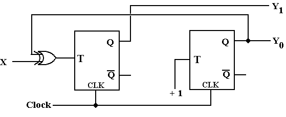
Consider the following circuit. We want to discover what it does.
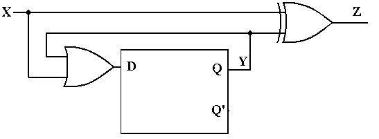
Figure: Circuit to Be Analyzed
Step 1: Identify and Label the Inputs, Outputs, and Internal States
We use the following variables in the analysis of this circuit with a single flip-flop. X denotes the input, Y denotes the output of the flip-flop (Y’ also), and Z the output of the circuit. If we had more than one flip-flop, we would label the flip-flop with a number beginning at 0 and use that as a subscript, so flip-flop 0 would have output Y0, etc.
Step 2: Determine the
Inputs and Outputs of the Flip-flops
The next step is to determine the equations for Z, the output, and D, the input to the flip-flop. By inspection, we determine the following for the equations:
Z = X Å Y
D = X + Y
Step 3: Construct the
We begin this state by recalling the characteristic table of each flip-flop that is used in the design. Here we have only one flip-flip, a D with a very simple characteristic table that is better represented as an equation: Q(t+1) = D – the next state is what you put in now.
Noting that Q(t) = Y (the state of a flip-flop is also its output) we construct the following Next-State diagram for the flip-flop, based on the characteristic table of a D flip-flop and the equation we derived for the D input: D = X + Y.
One simple caution here is that the input to a flip-flop is
a function of the present state only,
having nothing to do with the next state (as we have no crystal balls). Thus Y = Q(t).
Here is the present state (PS) / next state (NS) diagram for the circuit.
|
X |
Q(t) = Y |
D = X + Y |
Q(t+1) |
|
0 |
0 |
0 |
0 |
|
0 |
1 |
1 |
1 |
|
1 |
0 |
1 |
1 |
|
1 |
1 |
1 |
1 |
The output table is similarly constructed, using the equation Z = X Å Y = Z = X Å Q(t). Again, note that the output is not a function of the next state.
|
X |
Q(t) |
Z |
|
0 |
0 |
0 |
|
0 |
1 |
1 |
|
1 |
0 |
1 |
|
1 |
1 |
0 |
These two tables are combined to form the transition / output table.
|
X |
Q(t) = Y |
D = X + Y |
Q(t+1) / Z |
|
0 |
0 |
0 |
0 / 0 |
|
0 |
1 |
1 |
1 / 1 |
|
1 |
0 |
1 |
1 / 1 |
|
1 |
1 |
1 |
1 / 0 |
At this point, we should produce a state table in the standard format. This involves assigning labels to each of the two states, currently identified only as Q(t) = 0 and Q(t) = 1. For lack of anything more imaginative, we label the states 0 and 1.
|
|
Next State/Output |
|
|
|
X = 0 |
X = 1 |
|
0 |
0 / 0 |
1 / 1 |
|
1 |
1 / 1 |
1 / 0 |
Figure: State Table for Circuit to be Analyzed
Step 4: Construct the
State Diagram
The final step in the process may be the creation of the state diagram.
At this point, we have a complete description of the circuit. It may be possible to proceed from this diagram to obtain an understanding of what the circuit does.
Step 5: If possible,
identify the circuit.
This circuit is a 2–state device, with memory represented by one bit. The circuit stays in state 0 from the start until a 1 is input at which time it transitions to state 1 and remains there. Note the relation of the output to the input, depending on the state of the machine.
Input Q(t) Output
0 0 0 For Q(t) = 0, the output is X
1 0 1
0 1 1 For Q(t) = 1, the output is X’.
1 1 0
A verbal description of the circuit is then that it copies its input to the output until the first 1 is encountered in the input stream. After that event, all input is output as complemented.
What this circuit does is take the two’s-complement of a binary integer, presented to the circuit least-significant bit first. It is easy to prove that such a strategy produces the two’s complement of a number. First, consider a number ending in 1, say XnXn-1…. X2X11.
The one’s complement of this number is Xn’Xn-1’ …. X2’X1’0. Adding 1 to this produces the number Xn’Xn-1’ …. X2’X1’1, in which the least significant 1 is copied and the remaining bits are complemented. The proof is completed by supposing that the number terminates in one or more zeroes; i.e., its least significant bits are 10 …. 0, where the count of zeroes is not important. The one’s-complement of this number will end with 01 …. 1, where each zero in the original has turned to a 1. But 01 …. 1 + 1 = 10 …. 0, and up to the least significant 1 the two’s-complement is a copy of the bits in the integer itself. Note that there is no carry out of the addition that produced the right-most 1, so the remainder of the integer is formed by the one’s-complement. Thus we have a complete description of the circuit.
It is a serial two’s–complementer.
Design of
Sequential Circuits
Having seen how to analyze digital circuits, we now investigate how to design digital circuits. We assume that we are given a complete and unambiguous description of the circuit to be designed as a starting point. At this level, most design problems focus on one of two topics: modulo-N counters and sequence detectors.
Here is an overview of the design procedure for a sequential circuit.
1) Derive the state
diagram and state table for the circuit.
2) Count
the number of states in the state diagram (call it N) and calculate the
number of flip-flops needed
(call it P) by solving the equation
2P-1 < N £ 2P. This is best solved by guessing the value of
P.
3) Assign
a unique P-bit binary number (state vector) to each state.
Often, the first state = 0,
the next state = 1, etc.
4) Derive
the state transition table and the output table.
5) Separate
the state transition table into P tables, one for each flip-flop.
WARNING: Things can get messy
here; neatness counts.
6) Decide
on the types of flip-flops to use. When
in doubt, use all JK’s.
7) Derive
the input table for each flip-flop using the excitation tables for the type.
8) Derive
the input equations for each flip-flop based as functions of the input
and current state of all
flip-flops.
9) Summarize
the equations by writing them in one place.
10) Draw
the circuit diagram. Most homework
assignments will not go this far,
as the circuit diagrams are
hard to draw neatly.
Design Problem: A Modulo-4 Counter
As our first design problem, let’s consider a modulo-four counter. When the direction is not specified, we usually intend to build a modulo-four up-counter: 0, 1, 2, 3, 0, 1, 2, 3, etc. We solve these design problems by using the step-wise procedure listed above.
Step 1: Derive the
state diagram and state table for the circuit.
Here is the state diagram. Note that it is quite simple and involves no input.
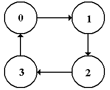
Figure: The State Diagram for a Modulo-4 Up Counter
The state table is simply a rearrangement of the state diagram into a tabular form.
|
|
|
|
0 |
1 |
|
1 |
2 |
|
2 |
3 |
|
3 |
0 |
Step 2: Count the number of states in the
state diagram (call it N) and calculate the
number of flip-flops needed
(call it P) by solving the equation 2P-1 < N £ 2P.
The number of states on a modulo-N counter is simply N;
these are labeled 0 through
(N – 1). Specifically, a modulo-4
counter has four states: labeled 0, 1, 2, and 3.
We solve the equation 2P-1 < 4 £ 2P by noting that 21 = 2 and 22 = 4, so we have determined that 21 < 4 £ 22, hence P = 2. We shall see later that there are valid solutions with more than two flip-flops, but there are none with fewer.
Step 3 Assign a unique P-bit binary number (state
vector) to each state.
Often, the first state = 0,
the next state = 1, etc.
Some sequential circuits suggest an innovative numbering system, but modulo–N counters never do. We go with the obvious labeling, generated by assigning each decimal number its two-bit binary equivalent as an unsigned integer in the range from 0 to 3.
|
State |
2-bit Vector |
|
0 |
0 0 |
|
1 |
0 1 |
|
2 |
1 0 |
|
3 |
1 1 |
Step 4 Derive the state transition table and the
output table.
There is no output table for any modulo–N counter, as the output associated with this type of table is the output on a transition, as is seen in a sequence detector. The transition table is a direct translation of the state table, using the assignments from the previous step.
|
|
|
|
|
0 |
00 |
01 |
|
1 |
01 |
10 |
|
2 |
10 |
11 |
|
3 |
11 |
00 |
Step 5 Separate the state transition table into P
tables, one for each flip-flop.
Here we separate the state transition table into 2 tables, one for each flip-flop. Note that the flip-flops will be numbered 0 and 1, with flip-flop 0 storing the least significant bit of the state information. Thus, we shall refer to the state information as Y1Y0.
|
Flip-Flop 1 |
|
Flip-Flop 0 |
||
|
|
|
|
|
|
|
Y1 Y0 |
Y1(T+1) |
|
Y1 Y0 |
Y0(T+1) |
|
0 0 |
0 |
|
0 0 |
1 |
|
0 1 |
1 |
|
0 1 |
0 |
|
1 0 |
1 |
|
1 0 |
1 |
|
1 1 |
0 |
|
1 1 |
0 |
Step 6 Decide on the types of flip-flops to use. When in doubt, use all JK’s.
Up to this point, we have made no assumptions about the type of flip-flop to use. In order to proceed any farther with the design, we must now commit to a specific type. In line with this author’s preferences, he chooses to use two JK flip-flops.
|
Q(t) |
Q(t+1) |
J |
K |
|
0 |
0 |
0 |
d |
|
0 |
1 |
1 |
d |
|
1 |
0 |
d |
1 |
|
1 |
1 |
d |
0 |
The excitation table for a JK flip-flop is shown at right. Recall that the “d” stands for “Don’t Care”. For example, if we have Q(t) = 0 and want Q(t+1) = 0, we can use either J = 0, K = 0 or J = 0, K = 1. Similarly either J = 1 and K = 0 or J = 1 and K = 1 will take Q(t) = 0 to Q(t + 1) = 1.
Step 7 Derive the input table for each flip-flop
using the excitation tables for the type.
First look at flip-flop 1, representing the high-order bit. Note that we compare the present state of Y1 to its next state in order to determine J1 and K1.
|
PS |
NS |
Input |
|
|
Y1 Y0 |
Y1 |
J1 |
K1 |
|
0 0 |
0 |
0 |
d |
|
0 1 |
1 |
1 |
d |
|
1 0 |
1 |
d |
0 |
|
1 1 |
0 |
d |
1 |
Note that in deciding on the input, we must match only the
0’s and 1’s. We ignore the
don’t–cares. Note that the “d” for
“don’t–care” is not a variable to be assigned a value. It is a value that does not need to be
matched. At the moment, Y0 is
included in the table for future use only.
It plays no part in determining the values of J1 and K1.
Here is the table for Y0
|
PS |
NS |
Input |
|
|
Y1 Y0 |
Y0 |
J0 |
K0 |
|
0 0 |
1 |
1 |
d |
|
0 1 |
0 |
d |
1 |
|
1 0 |
1 |
1 |
d |
|
1 1 |
0 |
d |
1 |
Again, Y1 is included in the table for future use only. It plays no part in determining the values of J0 and K0.
Step 8 Derive the input equations for each flip-flop
based as functions of the input
and current state of all
flip-flops.
At this point, we try to derive an expression that matches
each column. Formal methods can be used,
but generally are more trouble than they are worth. Here is this author’s set of rules to match
an expression to a given column.
1) If a column does not have a 0 in it, match it to the
constant value 1.
If a column does
not have a 1 in it, match it to the constant value 0.
2) If the column has both 0’s and 1’s in
it, try to match it to a single variable,
which must be part
of the present state. Only the 0’s and
1’s in a column
must match the
suggested function.
3) If every 0 and 1 in the column is a
mismatch, match to the complement
of a function.
4) If all the above fails, try for simple combinations of the
present state.
Let’s look at the input table for Y1.
|
PS |
NS |
Input |
|
|
Y1 Y0 |
Y1 |
J1 |
K1 |
|
0 0 |
0 |
0 |
d |
|
0 1 |
1 |
1 |
d |
|
1 0 |
1 |
d |
0 |
|
1 1 |
0 |
d |
1 |
Note that the column for J1 has a 0 and a 1 in it as does the column for K1. Each column has two “don’t cares” in it, but we ignore these. Because each column has both a 0 and a 1 in it, neither is a match for a constant function. We now try to match J1.
J1
does not match Y1, because Y1 is 0 in the same row (0 1)
as J1 is 1.
J1 matches Y0. In row 0 0, both Y0 and J1
are 1. In row 0 1, both Y0
and J1 are 1.
In rows 1 0 and 1 1, J1
is a “don’t care”, so we do not need to match it.
Similar logic shows that K1 matches Y0 also.
So now we have the following matches for J1 and K1.
|
PS |
NS |
Input |
|
|
Y1 Y0 |
Y1 |
J1 |
K1 |
|
0 0 |
0 |
0 |
d |
|
0 1 |
1 |
1 |
d |
|
1 0 |
1 |
d |
0 |
|
1 1 |
0 |
d |
1 |
J1 = Y0 K1 = Y0
We now examine Y0
|
PS |
NS |
Input |
|
|
Y1 Y0 |
Y0 |
J0 |
K0 |
|
0 0 |
1 |
1 |
d |
|
0 1 |
0 |
d |
1 |
|
1 0 |
1 |
1 |
d |
|
1 1 |
0 |
d |
1 |
Note that there are no 0’s in either the J0 or K0
column. The simplest (and best) match is
J0 = 1 and K0 = 1.
Step 9 Summarize the equations by writing them in one
place.
Here they are.
J1
= Y0 K1 =
Y0
J0 = 1 K0
= 1
This is a counter, so there is no Z output.
Step 10 Draw the circuit
diagram.
But wait – there is another solution hidden here. Recall that a JK flip-flop can be used to emulate a T flip-flop by setting the J input equal to the K input. Note that the design has the following interesting property.
J1 = K1 = Y0
J0 = K0
= 1
Given this, we can replace each JK flip-flop with a T flip-flop, arriving at this design.
The modulo–4 counter just designed outputs binary codes for the time pulses. Specifically, we assume that it is initialized to Y1Y0 = 00 and then outputs 01, 10, 11, 00, 01, 10, 11, etc. A more realistic circuit would output discrete pulses corresponding to the decoded output, so that first T0 = 1 and all others are 0, then T1 = 1 and all others are 0, etc. In order to produce the discrete signals T0, T1, T2, and T3, we need to add a decoding phase to the counter.
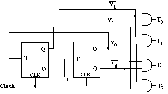
Note that the above design is simplified by the fact that the outputs Y1’ and Y0’ are available directly from the flip-flops and do not need to be synthesized using NOT gates.
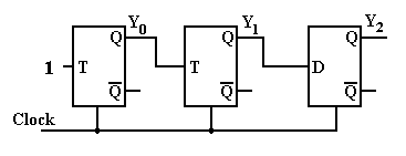
One can achieve a simpler design at the cost of additional flip-flops. The following design is called a one-hot design, in that it uses a shift register in which exactly one flip-flop at a time is storing a 1. This design also works as a modulo-4 counter and skips the decoder delays.
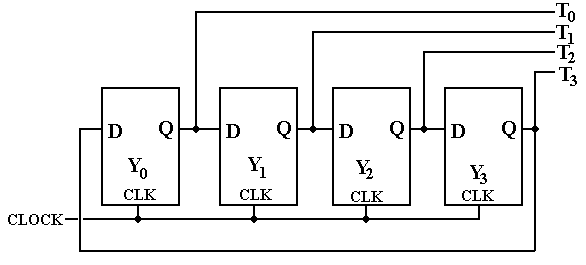
When the counter is initialized, we set Y0 = 1, and Y1 = Y2 = Y3 = 0. As the clock ticks, the single 1 is shifted by the shift register, so that the discrete signals become high in sequence.
Another Design
Problem: The Modulo-4 Up-Down Counter
For the next design, we introduce a problem that uses input. This is a modulo-4 up-down counter. The input X is used to control the direction of counting.
If X = 0, the device counts up: 0, 1, 2, 3, 0, 1, 2, 3, etc.
If X = 1, the device counts
down: 0, 3, 2, 1, 0, 3, 2, 1, etc.
Step 1: Derive the
state diagram and state table for the circuit.
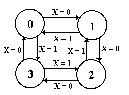
The state diagram for the modulo-4 up-down counter is shown at right. Notice that the X input is used to determine the counting direction. Again, this type of circuit does not have any output associated with the transitions; the output just reflects which of the four states the machine finds itself in at the moment.
We now produce the sate table by translating the state diagram. As an aside, some students might prefer to begin the design process with the state table and omit the state diagram. That is certainly acceptable practice; whatever works should be used.
Here, the state table depends on X – the input used to specify the counting direction.
|
|
|
|
|
|
X = 0 |
X = 1 |
|
0 |
1 |
3 |
|
1 |
2 |
0 |
|
2 |
3 |
1 |
|
3 |
0 |
2 |
Step 2: Count the number of states in the
state diagram (call it N) and calculate the
number of flip-flops needed (call
it P) by solving the equation 2P-1 < N £
2P.
The number of states on a modulo-N counter is simply N;
these are labeled 0 through
(N – 1). Specifically, a modulo-4
counter has four states: labeled 0, 1, 2, and 3.
We solve the equation 2P-1 < 4 £ 2P by noting that 21 = 2 and 22 = 4, so we have determined that 21 < 4 £ 22, hence P = 2. We shall see later that there are valid solutions with more than two flip-flops, but there are none with fewer.
Step 3 Assign a unique P-bit binary number (state vector)
to each state.
Often, the first state = 0,
the next state = 1, etc.
Some sequential circuits suggest an innovative numbering system, but modulo-N counters never do. We go with the obvious labeling, generated by assigning each decimal number its two-bit binary equivalent as an unsigned integer in the range from 0 to 3.
|
State |
2-bit Vector |
|
0 |
0 0 |
|
1 |
0 1 |
|
2 |
1 0 |
|
3 |
1 1 |
Step 4 Derive the state transition table and the
output table.
There is no output table for any modulo-N counter, as the output associated with this type of table is the output on a transition, as is seen in a sequence detector. The transition table is a direct translation of the state table, using the assignments from the previous step.
The transition table for the modulo-4 up-down counter is as follows.
|
|
|
||
|
|
|
X = 0 |
X = 1 |
|
0 |
00 |
01 |
11 |
|
1 |
01 |
10 |
00 |
|
2 |
10 |
11 |
01 |
|
3 |
11 |
00 |
10 |
Step 5 Separate the state transition table into P
tables, one for each flip-flop.
Here we separate the state transition table into 2 tables, one for each flip-flop. Note that the flip-flops will be numbered 0 and 1, with flip-flop 0 storing the least significant bit of the state information. Thus, we shall refer to the state information as Y1Y0.
|
Flip-Flop 1 |
|
Flip-Flop 0 |
||||
|
PS |
|
|
PS |
|
||
|
Y1Y0 |
Y1, X = 0 |
Y1, X = 1 |
|
Y1Y0 |
Y0, X = 0 |
Y0, X = 1 |
|
0 0 |
0 |
1 |
|
0 0 |
1 |
1 |
|
0 1 |
1 |
0 |
|
0 1 |
0 |
0 |
|
1 0 |
1 |
0 |
|
1 0 |
1 |
1 |
|
1 1 |
0 |
1 |
|
1 1 |
0 |
0 |
The student who is paying attention at this point will notice an interesting feature concerning flip–flop 0; specifically that its next state does not depend on X. This is due to the fact that in considering a modulo–N counter for N an even number, one moves from odd numbers to even numbers and from even numbers to odd numbers in both counting up and counting down. If N is odd, there is a transition between (N – 1), an even number, and 0 (also even).
Step 6 Decide on the types of flip-flops to use. When in doubt, use all JK’s.
Up to this point, we have made no assumptions about the type of flip-flop to use. In order to proceed any farther with the design, we must now commit to a specific type. In line with this author’s preferences, he chooses to use two JK flip-flops.
|
Q(t) |
Q(t+1) |
J |
K |
|
0 |
0 |
0 |
d |
|
0 |
1 |
1 |
d |
|
1 |
0 |
d |
1 |
|
1 |
1 |
d |
0 |
The excitation table for a JK flip-flop is shown at right. Recall that the “d” stands for “Don’t Care”. For example, if we have Q(t) = 0 and want Q(t+1) = 0, we can use either J = 0, K = 0 or J = 0, K = 1. Similarly either J = 1 and K = 0 or J = 1 and K = 1 will take Q(t) = 0 to Q(t + 1) = 1.
Step 7 Derive the input table for each flip-flop
using the excitation tables for the type.
Here is the input table for flip-flop 1. Note that the arrangement of the table has been altered to reflect the fact that we now have a binary input.
|
|
X = 0 |
X = 1 |
||||
|
Y1Y0 |
Y1 |
J1 |
K1 |
Y1 |
J1 |
K1 |
|
0 0 |
0 |
0 |
d |
1 |
1 |
d |
|
0 1 |
1 |
1 |
d |
0 |
0 |
d |
|
1 0 |
1 |
d |
0 |
0 |
d |
1 |
|
1 1 |
0 |
d |
1 |
1 |
d |
0 |
Here is the input table for flip-flop 0.
|
|
X = 0 |
X = 1 |
||||
|
Y1Y0 |
Y0 |
J0 |
K0 |
Y1 |
J0 |
K0 |
|
0 0 |
1 |
1 |
d |
1 |
1 |
d |
|
0 1 |
0 |
d |
1 |
0 |
d |
1 |
|
1 0 |
1 |
1 |
d |
1 |
1 |
d |
|
1 1 |
0 |
d |
1 |
0 |
d |
1 |
Step 8 Derive the input equations for each flip-flop
based as functions of the input
and current state of all
flip-flops.
Again, we try to derive an expression that matches each
column. Formal methods can be used, but
generally are more trouble than they are worth.
Here is this author’s set of rules to match an expression to a given
column.
1) If a column does not have a 0 in it, match it to the
constant value 1.
If a column does
not have a 1 in it, match it to the constant value 0.
2) If the column has both 0’s and 1’s in
it, try to match it to a single variable,
which must be part
of the present state. Only the 0’s and
1’s in a column
must match the
suggested function.
3) If every 0 and 1 in the column is a
mismatch, match to the complement
of a function.
4) If all the above fails, try for simple combinations of the
present state.
The reader will note that there are two columns for each
variable for which an equation is desired; one column for X = 0 and one column
for X = 1. For example, consider the
table for flip-flop 0, just above. If we
work on a column-by column basis, we shall arrive at four equations. One for J0 when X = 0,
one for K0
when X = 0,
one for J0
when X = 1, and
one for K0
when X = 1.
However, we need a single equation for J0 and a single equation for K0.
The Combine Rule
There are many ways to produce the single equations for J0 and K0, including algebraic simplification and Karnaugh Maps. The method preferred by this author for producing a single equation for an entity such as J0 or K0 is as follows.
1. Use the “least
complexity” matching rule as described above for each column of
the expression. Thus, for J0, we shall have two
expressions, one for X = 0 and one
for X = 1.
2. Use this author’s “combine rule” to produce a single expression.
The rule for combining expressions derived separately for X = 0 and X = 1 is
X’·(expression for X= 0) + X·(expression for X = 1).
The origin of the combination rule is the following
observation. Consider the Boolean
expression F = X’·A
+ X·B,
where A and B are any Boolean expressions.
When X = 0, this becomes F = 1·A + 0·B =
A, and
when X = 1, this becomes F = 0·A + 1·B =
B.
We then see that F = X’·A + X·B if and only if F = A when X = 0 and F = B when X = 1. This simple observation is the source of the combination rule. It will always produce a correct result and usually produce the simplest result.
There are quite a few simplifications of the combine rule, all of which should be noted.
1. A = B. Then F = X’·A + X·A = A
2. A
= 0. Then F = X’·0 + X·B = X·B
B = 0 Then F = X’·A + X·0 = X’·A
3. A
= 1 Then F = X’·1 + X·B =
X’ + B (by the Absorption Theorem)
B = 1 Then F = X’·A + X·1 = A + X (also by the Absorption Theorem)
The last two statements seem somewhat surprising, so we prove them.
a) X’ + X·B
= X’ + B
If X = 0, then X’ + X·B = 1
+ 0·B
=1
X’
+ B = 1 + B = 1
If X = 1, then X’
+ X·B
= 0 + 1·B
= B
X’
+ B = 0 + B = B
b) X’·A
+ X = A + X
If X = 0, then X’·A + X = 1·A + 0
= A
A
+ X = A + 0 = A
If X = 1, then X’·A + X = 0·A + 1
= 1
A
+ X = A + 1 = 1
So we get to work with the combine rule.
The table for flip-flop 1 is as follows.
|
|
X = 0 |
X = 1 |
||||
|
Y1Y0 |
Y1 |
J1 |
K1 |
Y1 |
J1 |
K1 |
|
0 0 |
0 |
0 |
d |
1 |
1 |
d |
|
0 1 |
1 |
1 |
d |
0 |
0 |
d |
|
1 0 |
1 |
d |
0 |
0 |
d |
1 |
|
1 1 |
0 |
d |
1 |
1 |
d |
0 |
J1
= Y0 J1
= Y0’
K1
= Y0 K1
= Y0’
We arrived at the matches for X = 0 by noting that each column had both a 0 and a 1. The next step is to try matches against the variables. Y1 is not a match, but Y0 is.
We arrived at the matches for X = 1 by noting that each column also had both a 0 and a 1. None of the simple variables matched, but we noted that Y0’ matched both.
We now apply the combine
rule: X’·(expression
for X= 0) + X·(expression
for X = 1).
For X = 0 J1 = Y0, and for X = 1 J1 = Y0’, so J1 = X’·Y0 +
X·Y0’ =
X Å Y0.
For X = 0 K1 = Y0, and for X = 1 K1 = Y0’, so K1 = X’·Y0 +
X·Y0’ =
X Å Y0.
The table for flip-flop 0 is as follows.
|
|
X = 0 |
X = 1 |
||||
|
Y1Y0 |
Y0 |
J0 |
K0 |
Y1 |
J0 |
K0 |
|
0 0 |
1 |
1 |
d |
1 |
1 |
d |
|
0 1 |
0 |
d |
1 |
0 |
d |
1 |
|
1 0 |
1 |
1 |
d |
1 |
1 |
d |
|
1 1 |
0 |
d |
1 |
0 |
d |
1 |
J0 = 1 J0 = 1
K0 = 1 K0 = 1
We now apply the combine
rule: X’·(expression
for X= 0) + X·(expression
for X = 1).
This is easy. J0 = X’·1 + X·1 = X’ + X = 1
This is easy. K0 = X’·1 + X·1 = X’ + X = 1
Step 9 Summarize the equations by writing them in one
place.
Here they are.
J1
= X Å Y0 K1 = X Å Y0
J0 = 1 K0 = 1
This is a counter, so there is no Z output.
Step 10 Draw the circuit
diagram.
Again, we note that both flip-flops have J = K, so we can replace each by a T flip-flop.
Several other obvious solutions exist for the up–down counter, including one that is a copy of the one–hot solution in which the X input controls the shift direction: X = 0 for shift right and X = 1 for shift left. Students are invited to examine these solutions at their leisure.
The Prize Problem
For several semesters I have had a prize problem that nobody (including myself) can solve. The goal of the problem is to demonstrate at least one instance in which the combine rule does not produce the simplest solution. Here is the problem.
Do a design with one or more JK flip-flops (note – one should be enough). Use the methods of these notes – least complexity search and combine rule – to produce a solution for J and K. Demonstrate a method that produces simpler Boolean expressions for J and K. Any student who wants to attempt the problem is advised to consult with me before undertaking this problem to avoid wasting time in solving the wrong problem.
The Traffic Light
Problem
As a more complex digital design problem, we shall consider the controller for a simple traffic light. The light is at the intersection of two roads, one (NS) running North-South and one (EW) running East-West. The light should be considered as two coupled traffic lights, one called L1 and the other L2. Each of the lights (or pairs of lights) displays the standard sequence: Red, Green, Yellow. More complex traffic lights, such as those with turn signals or advanced green lights, can be similarly modeled – but let’s keep it simple.
We see that there are six states in the system. In line with standard binary notation, I begin the labeling with state 0. It will be convenient to have state 0 be a Red-Red state, thus:
|
State |
Light 1 |
Light 2 |
Alias |
|
0 |
Red |
Red |
RR |
|
1 |
Red |
Green |
RG |
|
2 |
Red |
Yellow |
RY |
|
3 |
Red |
Red |
RR |
|
4 |
Green |
Red |
GR |
|
5 |
Yellow |
Red |
YR |
Before continuing with the design, we note that there are two states, 0 and 3, with the alias RR. We use this fact to comment on an alternate design, one which I decline to use.
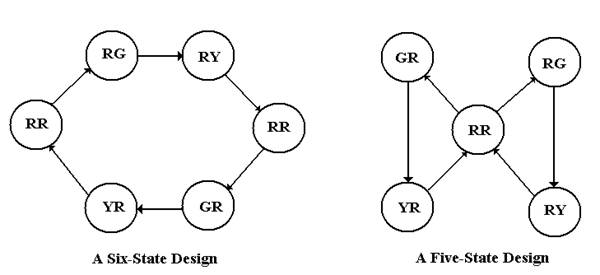
At first look, the design on the right appears simpler, only having five states. The diagram at right hides one specific difficulty – the state that follows RR. Is it GR or RG? The design at right calls for the transition RR => RG to alternate with the transition RR => GR; thus we would need a flip-flop to remember which transition was taken last time. Each of the two designs requires at least three flip-flops. We go with the easier design on the left.
At this point, we complete step 1 of our design process by deriving the state table for the circuit. Note that the circuit does not have any input labeled X – the only input is the clock.
|
|
|
||
|
Number |
Alias |
Number |
Alias |
|
0 |
RR |
1 |
RG |
|
1 |
RG |
2 |
RY |
|
2 |
RY |
3 |
RR |
|
3 |
RR |
4 |
GR |
|
4 |
GR |
5 |
YR |
|
5 |
YR |
0 |
RR |
The table at right is the state table, with the state number and alias given for both the present and next state. We keep the alias for convenience only as we have not resolved the duplicate “RR” alias. At this point, we note that we have six states and are ready for Step 2: Count the Flip-Flops.
We need to use three flip-flops; P = 3.
Step 3: Assign a Binary Number to Each State
The solution here is obvious – we treat each number as a three-bit unsigned integer and assign the binary numbers 000, 001, 010, 011, 100, and 101. At this point, we have two binary patterns that are not assigned 110 (state 6) and 111 (state 7). Although these states are supposedly unreachable in our design, I propose to handle them anyway as we are designing a device that is safety-critical. This design specifies that the next state following either state 6 or state 7 will be state 0. As a safety consideration, we further specify that both states 6 and state 7 display Red on each of the two lights as we consider these to be failure states.
Following our standard design practice, we label the flip-flops with the integers 2, 1, and 0, and call the outputs of the flip-flops Q2, Q1, and Q0, as Y is taken to stand for Yellow.
Step 4: Derive the State Transition Table and Output Table.
The first step in deriving the output table is to define the output. The design calls for two coupled traffic lights, each with the standard colors Red, Green, and Yellow. The circuit will thus have six outputs R1, G1, Y1, R2, G2, and Y2 – the first three outputs to light 1 and the second three outputs to light 2. The output table is somewhat complicated.
|
|
Alias |
Q2Q1Q0 |
R1 |
G1 |
Y1 |
R2 |
G2 |
Y2 |
|
0 |
RR |
0 0 0 |
1 |
0 |
0 |
1 |
0 |
0 |
|
1 |
RG |
0 0 1 |
1 |
0 |
0 |
0 |
1 |
0 |
|
2 |
RY |
0 1 0 |
1 |
0 |
0 |
0 |
0 |
1 |
|
3 |
RR |
0 1 1 |
1 |
0 |
0 |
1 |
0 |
0 |
|
4 |
GR |
1 0 0 |
0 |
1 |
0 |
1 |
0 |
0 |
|
5 |
YR |
1 0 1 |
0 |
0 |
1 |
1 |
0 |
0 |
|
6 |
RR |
1 1 0 |
1 |
0 |
0 |
1 |
0 |
0 |
|
7 |
RR |
1 1 1 |
1 |
0 |
0 |
1 |
0 |
0 |
It may seem that we have six signals to generate based on the three binary values Y2, Y1, and Y0, but we take a short-cut. We note that each light is either Red, Green, or Yellow, and when it is not either Green or Yellow it must be Red. Thus, the only signals we generate directly are G1, Y1, G2, and Y2.
Here are the output equations
G1 = Q2·Q1’·Q0’ G2 = Q2’·Q1’·Q0
Y1 = Q2·Q1’·Q0 Y2 = Q2’·Q1·Q0’
R1 = (G1 + Y1)’ R2 = (G2 + Y2)’
If we wanted to provide extra fault tolerance, we would
demand that when one light is either green or yellow, the other must be red,
thus generating the equations
R1 = (G1 + Y1)’ + G2 + Y2 and
R2 = (G2 + Y2)’ + G1 + Y1
A bit of reflection will show that, even with this design, it is possible for one light to show more than one color. Here we assume a person seeing both red and green on a traffic light would assume something is very wrong.
We now consider the state transition table expressed in terms of Q2, Q1, and Q0.
|
|
|
|
|
|
Q2Q1Q0 |
Q2Q1Q0 |
|
0 |
0 0 0 |
0 0 1 |
|
1 |
0 0 1 |
0 1 0 |
|
2 |
0 1 0 |
0 1 1 |
|
3 |
0 1 1 |
1 0 0 |
|
4 |
1 0 0 |
1 0 1 |
|
5 |
1 0 1 |
0 0 0 |
|
6 |
1 1 0 |
0 0 0 |
|
7 |
1 1 1 |
0 0 0 |
Before breaking this into three tables, one for each flip-flop, we note the handling of the supposedly non-reachable states 6 and 7. The design here is based on fault tolerance, the idea that the circuit should have some ability to restore itself from faulty operation.
Admittedly, the strategy reflected in this design may not be realistic. It is shown mostly to draw the student’s attention to the concepts and not to present an optimal solution.
Step 5: Separate the Table into Three Tables, One for Each
Flip-Flop
Remember that each table must have a complete description of the present state.
|
Q2 |
|
Q1 |
|
Q0 |
|||
|
PS |
NS |
|
PS |
NS |
|
PS |
NS |
|
Q2Q1Q0 |
Q2 |
|
Q2Q1Q0 |
Q1 |
|
Q2Q1Q0 |
Q0 |
|
0 0 0 |
0 |
|
0 0 0 |
0 |
|
0 0 0 |
1 |
|
0 0 1 |
0 |
|
0 0 1 |
1 |
|
0 0 1 |
0 |
|
0 1 0 |
0 |
|
0 1 0 |
1 |
|
0 1 0 |
1 |
|
0 1 1 |
1 |
|
0 1 1 |
0 |
|
0 1 1 |
0 |
|
1 0 0 |
1 |
|
1 0 0 |
0 |
|
1 0 0 |
1 |
|
1 0 1 |
0 |
|
1 0 1 |
0 |
|
1 0 1 |
0 |
|
1 1 0 |
0 |
|
1 1 0 |
0 |
|
1 1 0 |
0 |
|
1 1 1 |
0 |
|
1 1 1 |
0 |
|
1 1 1 |
0 |
Step 6 – Select the Flip-Flop Type and Copy Its
Excitation Table
Since the JK flip-flops seem to be the Q(t) Q(t + 1) J K
most useful type, I have selected to 0 0 0 d
use JK’s in the design. As a reminder 0 1 1 d
I have written the excitation table for 1 0 d 1
this flip-flop to the right. 1 1 d 0
Step 7 – Derive the Input Table for Each Flip-Flop
|
Flip-Flop 2 |
|
Flip-Flop 1 |
|
Flip-Flop 0 |
|||||||||
|
PS |
NS |
Input |
|
PS |
NS |
Input |
|
PS |
NS |
Input |
|||
|
Q2Q1Q0 |
Q2 |
J2 |
|
|
Q2Q1Q0 |
Q1 |
J1 |
K1 |
|
Q2Q1Q0 |
Q0 |
J0 |
K0 |
|
0 0 0 |
0 |
0 |
d |
|
0 0 0 |
0 |
0 |
d |
|
0 0 0 |
1 |
1 |
d |
|
0 0 1 |
0 |
0 |
d |
|
0 0 1 |
1 |
1 |
d |
|
0 0 1 |
0 |
d |
1 |
|
0 1 0 |
0 |
0 |
d |
|
0 1 0 |
1 |
d |
0 |
|
0 1 0 |
1 |
1 |
d |
|
0 1 1 |
1 |
1 |
d |
|
0 1 1 |
0 |
d |
1 |
|
0 1 1 |
0 |
d |
1 |
|
1 0 0 |
1 |
d |
0 |
|
1 0 0 |
0 |
0 |
d |
|
1 0 0 |
1 |
1 |
d |
|
1 0 1 |
0 |
d |
1 |
|
1 0 1 |
0 |
0 |
d |
|
1 0 1 |
0 |
d |
1 |
|
1 1 0 |
0 |
d |
1 |
|
1 1 0 |
0 |
d |
1 |
|
1 1 0 |
0 |
0 |
d |
|
1 1 1 |
0 |
d |
1 |
|
1 1 1 |
0 |
d |
1 |
|
1 1 1 |
0 |
d |
1 |
Step 8 – Derive the Input Equation for Each Flip-Flop
J2 = Q1
·
Q0 J1
= Q2’ ·
Q0 J0
= Q2’ + Q1’
Step 9 – Summarize the Equations
Not needed – there are no other equations.
Step 10 – Draw the Circuit
The circuit is shown on the next page of the notes. The diagram has three parts.
1) The middle
part is the design from steps 8 and 9 of the above work. It shows the
design of what is essentially
a modulo-6 counter.
2) The top part
contains the circuits that implement the equations for R1, Y1, G1, etc. as
found in the first part of
step 4 of the design. This is
essentially the output of the
circuit –
six signals that control six traffic lights.
3) The bottom part of the circuit
is what provides clock pulses to the modulo-6 counter.
Note that the circuit is a
shift register used to provide a clock pulse at irregular
intervals: at T = 1, T = 6,
and T = 8, providing for unequal length of light phases.
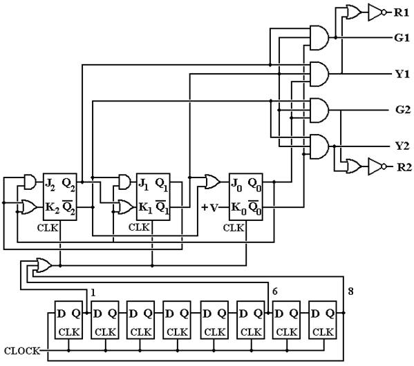
In this design, the input CLOCK is a regular signal, say one tick per second. The shift register at the bottom of the diagram shifts a single 1 around in a circular pattern, causing an output at T = 1, T = 6, and T = 8 (or 0). It is this irregular output that causes the modulo-6 counter in the middle of the diagram to move to the next state. We postulate that the circuit begins in state 0 (RR) and moves as follows.
|
State |
Alias |
Duration |
Ends at |
|
0 |
RR |
1 |
T = 1 |
|
1 |
RG |
5 |
T = 6 |
|
2 |
RY |
2 |
T = 8 (T = 0) |
|
3 |
RR |
1 |
T = 1 |
|
4 |
GR |
5 |
T = 6 |
|
5 |
YR |
3 |
T = 8 (T = 0) |
Solved Problems
1. How many flip-flops are required for the following sequence detectors?
a) 10101010 an eight bit sequence
b) 11110000 an eight bit sequence
c) 110110 a six bit sequence
d) 1011 a four bit sequence
ANSWER: All of these involve the equation 2P-1
< N £ 2P.
a) Eight-bit
sequence, so N = 8 and P = 3. Three
flip-flops.
b) Another
eight-bit sequence. Three
flip-flops.
c) A
six-bit sequence, N = 6. 22 < 6 £ 23, so Three
flip-flops.
d) A four bit sequence, N = 4. 21
< 4 £ 22, so Two flip-flops.
2. Derive the state table for the following
circuit. Use the assignments
A = 00, B = 01, C = 10, and D = 11.
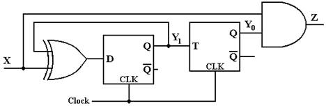
ANSWER: The first thing to do is to derive the
equations. These are obtained by examination
of the circuit diagram. Here are the
equations in my terminology.
Z = X · Y0
D1 = X Å Y1 Input is called D1 to
show that it is input to flip-flop 1.
T0 = Y1 Input is called T0
to associate it with flip-flop 0.
We now create a table that shows the inputs to the two flip-flops.
|
|
PS |
X = 0 |
X = 1 |
|||||
|
|
Y1 |
Y0 |
D1 |
T0 |
Z |
D1 |
T0 |
Z |
|
A |
0 |
0 |
0 |
0 |
0 |
1 |
0 |
0 |
|
B |
0 |
1 |
0 |
0 |
0 |
1 |
0 |
1 |
|
C |
1 |
0 |
1 |
1 |
0 |
0 |
1 |
0 |
|
D |
1 |
1 |
1 |
1 |
0 |
0 |
1 |
1 |
We now create two tables, one for each of the two flip-flops. We begin with the D flip-flop.
|
|
PS |
X = 0 |
X = 1 |
|||
|
|
Y1 |
Y0 |
D1 |
Q1(t + 1) |
D1 |
Q1(t + 1) |
|
A |
0 |
0 |
0 |
0 |
1 |
1 |
|
B |
0 |
1 |
0 |
0 |
1 |
1 |
|
C |
1 |
0 |
1 |
1 |
0 |
0 |
|
D |
1 |
1 |
1 |
1 |
0 |
0 |
Here is the table for the T flip-flop
|
|
PS |
X = 0 |
X = 1 |
|||
|
|
Y1 |
Y0 |
T0 |
Q0(t
+ 1) |
T0 |
Q0(t
+ 1) |
|
A |
0 |
0 |
0 |
0 |
0 |
0 |
|
B |
0 |
1 |
0 |
1 |
0 |
1 |
|
C |
1 |
0 |
1 |
1 |
1 |
1 |
|
D |
1 |
1 |
1 |
0 |
1 |
0 |
Here is the Next-State Table
|
|
PS |
X = 0 |
X = 1 |
|||
|
|
Y1 |
Y0 |
Y1(t
+ 1) |
Y0(t
+ 1) |
Y1(t
+ 1) |
Y0(t
+ 1) |
|
A |
0 |
0 |
0 |
0 |
1 |
0 |
|
B |
0 |
1 |
0 |
1 |
1 |
1 |
|
C |
1 |
0 |
1 |
1 |
0 |
1 |
|
D |
1 |
1 |
1 |
0 |
0 |
0 |
Here is the Output Table
|
|
PS |
X = 0 |
X = 1 |
|||
|
|
Y1 |
Y0 |
Z |
Z |
|
|
|
A |
0 |
0 |
0 |
0 |
|
|
|
B |
0 |
1 |
0 |
1 |
|
|
|
C |
1 |
0 |
0 |
0 |
|
|
|
D |
1 |
1 |
0 |
1 |
|
|
The Next State / Output Table with the binary numberings.
|
PS |
X = 0 |
X = 1 |
|
|
A |
0 0 |
0 0 / 0 |
1 0 / 0 |
|
B |
0 1 |
0 1 / 0 |
1 1 / 1 |
|
C |
1 0 |
1 1 / 0 |
0 1 / 0 |
|
D |
1 1 |
1 0 / 0 |
0 0 / 1 |
Here is the final form of the Next State/Output table
|
PS |
X = 0 |
X = 1 |
|
|
A |
A / 0 |
C / 0 |
|
|
B |
B / 0 |
D / 1 |
|
|
C |
D / 0 |
B / 0 |
|
|
D |
C / 0 |
A / 1 |
|
Here is a state diagram for the circuit.
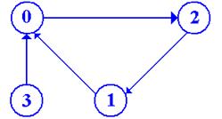
I cannot think what the circuit might do.
Does anyone have any ideas?
3. What does the following circuit do? More specifically, analyze the circuit and produce its state table and state diagram. Assume that the circuit starts at Y2Y1Y0 = 000.
ANSWER: We number the flip-flops left to right as 0, 1, 2
and produce the equations.
T0
= 1
T1
= Y0
D2
= Y1
We
now produce the next state table for the three flip-flops.
|
PS |
Next State |
|||||
|
Y0Y1Y2 |
T0 |
Y0 |
T1 |
Y1 |
D2 |
Y2 |
|
0 0 0 |
1 |
1 |
0 |
0 |
0 |
0 |
|
0 0 1 |
1 |
1 |
0 |
0 |
0 |
0 |
|
0 1 0 |
1 |
1 |
0 |
1 |
1 |
1 |
|
0 1 1 |
1 |
1 |
0 |
1 |
1 |
1 |
|
1 0 0 |
1 |
0 |
1 |
1 |
0 |
0 |
|
1 0 1 |
1 |
0 |
1 |
1 |
0 |
0 |
|
1 1 0 |
1 |
0 |
1 |
0 |
1 |
1 |
|
1 1 1 |
1 |
0 |
1 |
0 |
1 |
1 |
The
table above is correct, but not listed in proper order. Here is the table correctly arranged. This order is mandated by the bit ordering in
the question: Y2Y1Y0.
|
PS |
|
|
|
|
|
|
|
Y2Y1Y0 |
D2 |
Y2 |
T1 |
Y1 |
T0 |
Y0 |
|
0 0 0 |
0 |
0 |
0 |
0 |
1 |
1 |
|
0 0 1 |
0 |
0 |
1 |
1 |
1 |
0 |
|
0 1 0 |
1 |
1 |
0 |
1 |
1 |
1 |
|
0 1 1 |
1 |
1 |
1 |
0 |
1 |
0 |
|
1 0 0 |
0 |
0 |
0 |
0 |
1 |
1 |
|
1 0 1 |
0 |
0 |
1 |
1 |
1 |
0 |
|
1 1 0 |
1 |
1 |
0 |
1 |
1 |
1 |
|
1 1 1 |
1 |
1 |
1 |
0 |
1 |
0 |
We now produce the state table by removing the columns for
the D and T inputs and then by converting the binary numbers into decimal
numbers.
|
PS |
|
|
|
|
|
|
|
Y2Y1Y0 |
Y2 |
Y1 |
Y0 |
|
PS |
NS |
|
0 0 0 |
0 |
0 |
1 |
|
0 |
1 |
|
0 0 1 |
0 |
1 |
0 |
|
1 |
2 |
|
0 1 0 |
1 |
1 |
1 |
|
2 |
7 |
|
0 1 1 |
1 |
0 |
0 |
|
3 |
4 |
|
1 0 0 |
0 |
0 |
1 |
|
4 |
1 |
|
1 0 1 |
0 |
1 |
0 |
|
5 |
2 |
|
1 1 0 |
1 |
1 |
1 |
|
6 |
7 |
|
1 1 1 |
1 |
0 |
0 |
|
7 |
4 |
Here is the state diagram.
One must admit that it is a bit strange.
This is really a disguised modulo-4 counter, counting 1, 2,
7, 4, etc.
At this point, all that is required is the state diagram.
Should the student wonder what the instructor had in mind when designing the
circuit, the answer is that the circuit looked interesting. The instructor had no idea what the circuit
might do and still has no idea.
The main question is whether or not the student can apply a
well-defined procedure to a
well-defined problem.
4 Using two JK flip-flops, design a modulo-3 down-counter.
The only input to such a counter is
the clock. There are two outputs Y1Y0,
which take
values 10, 01, 00, 10, 01, 00
etc. Note that, unlike the homework, it
is counting down.
As a part of your design, produce the following.
a) The state diagram for the circuit.
b) The state table for the circuit.
c) The state transition table.
d) The input table for each flip-flop.
e) The input equations for each flip-flop.
ANSWER:
a) The state diagram for the circuit.
b) The state table for the circuit. It helps to read from the bottom up.
|
PS |
NS |
|
0 |
2 |
|
1 |
0 |
|
2 |
1 |
At this point, we note that we have 3 states, so need two flip-flops, as 21 < 3
£ 22. We must assign two bit numbers to each state:
obviously 0 => 00, 1 => 01, 2 => 10.
c) The state transition table.
|
PS |
NS |
|
|
0 |
0 0 |
1 0 |
|
1 |
0 1 |
0 0 |
|
2 |
1 0 |
0 1 |
We split this up into two tables, one for each flip-flop.
|
PS |
NS |
|
Y1
Y0 |
Y1 |
|
0 0 |
1 |
|
0 1 |
0 |
|
1 0 |
0 |
|
PS |
NS |
|
Y1
Y0 |
Y0 |
|
0 0 |
0 |
|
0 1 |
0 |
|
1 0 |
1 |
At this point, we could produce a solution using D
flip-flops. By inspection, we have
D1 = Y1’·Y0’
D0 = Y1·Y0’
The problem asks for solutions using JK flip-flops, so let’s
do that.
|
PS |
NS |
Input |
|
|
Y1 Y0 |
Y1 |
J1 |
K1 |
|
0 0 |
1 |
1 |
d |
|
0 1 |
0 |
0 |
d |
|
1 0 |
0 |
d |
1 |
|
PS |
NS |
Input |
|
|
Y1
Y0 |
Y0 |
J0 |
K0 |
|
0 0 |
0 |
0 |
d |
|
0 1 |
0 |
d |
1 |
|
1 0 |
1 |
1 |
d |
J1 = Y0’ J0
= Y1
K1 = 1 K0
= 1
COMMENT: A number of
students represented the tables in “reverse order”, as follows.
|
PS |
NS |
|
Y1
Y0 |
Y1 |
|
1 0 |
0 |
|
0 1 |
0 |
|
0 0 |
1 |
|
PS |
NS |
|
Y1
Y0 |
Y0 |
|
1 0 |
1 |
|
0 1 |
0 |
|
0 0 |
0 |
This is a perfectly acceptable solution and may be easier
to understand.
The most common error was to match the J and K inputs to
the next state values of Y1 and Y0; thus J1
matches the next state value of Y1.
This may be interesting, but is not useable as the circuits cannot
access any future values of the memory, but only the current values.
5. Design a modulo–3 down counter (2, 1, 0, 2,
1, 0, etc).
Use D flip–flops. Allow for the unused state 3 to transition to
state 0.
Do not draw the circuit; just show
the equations for the D inputs to the flip–flops.
ANSWER: First,
draw the state diagram.
Now produce the
state table
|
PS |
NS |
|
0 |
2 |
|
1 |
0 |
|
2 |
1 |
|
3 |
0 |
Count the States
and Flip–Flops
There
are four states, requiring two flip–flops: denoted Y1 and Y0.
Assign the Two–Bit
State Vectors
Obviously: 0 = 00 1 = 01 2
= 10 3 = 11
Derive the State Transition Table
|
Present State |
Next State |
|||
|
|
Y1 |
Y0 |
Y1 |
Y0 |
|
0 |
0 |
0 |
1 |
0 |
|
1 |
0 |
1 |
0 |
0 |
|
2 |
1 |
0 |
0 |
1 |
|
3 |
1 |
1 |
0 |
0 |
Produce Two
Tables, One for Each Flip–Flop
Y1:
|
PS |
NS |
|
|
Y1 |
Y0 |
Y1 |
|
0 |
0 |
1 |
|
0 |
1 |
0 |
|
1 |
0 |
0 |
|
1 |
1 |
0 |
Solution:
![]()
Y0:
|
PS |
NS |
|
|
Y1 |
Y0 |
Y0 |
|
0 |
0 |
0 |
|
0 |
1 |
0 |
|
1 |
0 |
1 |
|
1 |
1 |
0 |
Solution:
![]()
Problems for
Solution
1. Using two JK flip-flops and the methods of this chapter, design a
modulo-3 up-counter.
The only input to such a counter is
the clock. There are two outputs Y1Y0,
which take
values 00, 01, 10, 00, 01, 10, etc. As a part of your design, produce the
following.
a) The state diagram for the circuit.
b) The state table for the circuit.
c) The state transition table.
d) The input table for each flip-flop.
e) The input equations for each flip-flop.
f) A readable diagram for this circuit.
2. Extend the above circuit to produce three outputs Z0, Z1,
Z2, exactly one of which is
active (high) at any given clock
pulse.
3. Use three D flip-flops in a shift-register configuration to
produce the modulo-3 counter.
Include a start signal (START) that
sets the circuit to state 0, so Z0 = 1.
4. The following is a state transition table for a two-flip-flop
circuit with two inputs X1 and
X0. Design the circuit represented by this
transition table, using two JK flip-flops.
|
Present |
|
||||||||
|
State |
X1 = 0, X0 = 0 |
X1 = 0, X0 = 1 |
X1 = 1, X0 = 0 |
X1 = 1, X0 = 1 |
|||||
|
Y1 |
Y0 |
Y1 |
Y0 |
Y1 |
Y0 |
Y1 |
Y0 |
Y1 |
Y0 |
|
0 |
0 |
0 |
0 |
0 |
1 |
1 |
0 |
1 |
1 |
|
0 |
1 |
0 |
1 |
1 |
0 |
1 |
1 |
0 |
0 |
|
1 |
0 |
1 |
0 |
1 |
1 |
0 |
0 |
0 |
1 |
|
1 |
1 |
1 |
1 |
0 |
0 |
0 |
1 |
1 |
0 |
As a part of this design, provide the following.
a) Two state transition tables, one for each of the flip-flops.
b) Two input tables, one for each flip-flop.
c) The input equations for each flip-flop.
d) A readable design for this circuit.
5. The following is a state table for a circuit of interest.
|
|
|
|
|
|
X = 0 |
X = 1 |
|
A |
A/0 |
B/0 |
|
B |
A/0 |
C/0 |
|
C |
A/0 |
D/0 |
|
D |
A/1 |
D/0 |
Complete the design of this circuit, making the state vector assignments A = 00, B = 01, C = 10, and D = 11. Show the output table and output equation, as well as the input tables and equations for each of the two flip-flops. Draw the circuit. You may use either JK or D flip-flops.