Problem: Design a 11011 sequence detector using JK flip-flops. Allow overlap.
Step 1 – Derive the State Diagram and State Table for the Problem
The method to be used for deriving the state diagram depends on the problem. I show the method for a sequence detector. At this point in the problem, the states are usually labeled by a letter, with the initial state being labeled “A”, etc.
Step 1a – Determine the Number of States
It can be proven that an N-bit sequence detector requires at least N states to function correctly. It can also be shown that a circuit with more than N states is unnecessarily complicated and a waste of hardware; thus, an N-bit sequence detector has N states.
We are designing a sequence detector for a 5-bit sequence, so we need 5 states. We label these states A, B, C, D, and E. State A is the initial state.
Step 1b – Characterize Each State by What has been Input and What is Expected
State Has Awaiting
A -- 11011
B 1 1011
C 11 011
D 110 11
E 1101 1
Step 1c – Do the Transitions for the Expected Sequence
Here is a partial drawing of the state diagram. It has only the sequence expected. Note that the diagram returns to state C after a successful detection; the final 11 are used again.
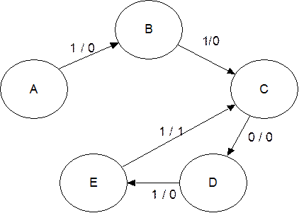
Note the labeling of the transitions: X / Z. Thus the expected transition from A to B has an input of 1 and an output of 0.
The transition from E to C has an output of 1 denoting that the desired sequence has been detected.
Step 1d – Insert the Inputs That Break the Sequence
Each state has two lines out of it – one line for a 1 and another line for a 0.
The notes below explain how to handle the bits that break the sequence.
A State A is the initial
state. It is waiting on a 1. If it gets a 0, the machine remains
in state A and continues to remain
there while 0’s are input.
B If state B gets a 0, the
last two bits input were “10”. This does
not begin the
sequence, so the machine goes back
to state A and waits on the next 1.
C If
state C gets a 1, the last three bits input were “111”. It can use the last two
of these 1’s to be the first two 1’s
of the sequence 11011, so the machine stays
in state C awaiting a 0. We might have something like 1111011, etc.
D If state D gets a 0, the
last four bits input were 1100. These 4
bits are not part of
the sequence, so we start over.
E If
state E gets a 0, the last five bits input were 11010. These five bits are not part of the
sequence, so start over.
More precisely we should be discussing prefixes and suffixes. At state C with input 111, the two bit suffix to the sequence input is 11 which is a two bit prefix of the desired sequence, so we stay at C. At E, getting a sequence 11010, we note that the 1–bit suffix is a 0, which is not a prefix of the desired sequence; the 2–bit suffix is 10, also not a prefix, etc.
Step 1e – Generate the State Table with Output
|
|
|
|
|
|
X = 0 |
X = 1 |
|
A |
A / 0 |
B / 0 |
|
B |
A / 0 |
C / 0 |
|
C |
D / 0 |
C / 0 |
|
D |
A / 0 |
E / 0 |
|
E |
A / 0 |
C / 1 |
Step 2 – Determine the Number of Flip-Flops Required
We have 5 states, so N = 5. We solve the equation 2P-1 < 5 £ 2P by inspection, noting that it is solved by P = 3. So we need three flip-flops.
Step 3 – Assign a unique P-bit binary number (state vector) to each state.
The simplest way is to make the following assignments
A = 000
B = 001
C = 010
D = 011
E = 100
Occasionally, a better assignment can be detected by
inspection of the next state table. I
note that the next states in the table cluster into two disjoint sets for X = 0
and X = 1.
For X = 0 the possible next
states are A and D
For X = 1 the possible next
states are B, C, and E.
For this reason, I elect to give even number assignments to
states A and D, and to give odd number assignments to states B, C, and E. Being somewhat traditional, I want to assign
the state numbers in increasing order so that we don’t get totally
confused. The assignment is
A = 000
B = 001
C = 011 Note that states 010, 110, and 111 are not
used.
D = 100
E = 101
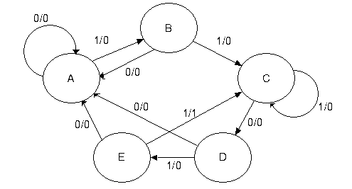
Step 4 – Generate the Transition Table With Output
Note that in many designs, such as counters, the states are already labeled with binary numbers, so the state table is the transition table. We shall label the internal state by the three bit binary number Y2Y1Y0 and use the three-bit vectors defined above.
|
|
|
||
|
|
|
X = 0 |
X = 1 |
|
|
Y2Y1Y0 |
Y2Y1Y0 / Z |
Y2Y1Y0 / Z |
|
A |
0 0 0 |
0
0 0 / 0 |
0
0 1 / 0 |
|
B |
0 0 1 |
0
0 0 / 0 |
0
1 1 / 0 |
|
C |
0 1 1 |
1
0 0 / 0 |
0
1 1 / 0 |
|
D |
1 0 0 |
0
0 0 / 0 |
1
0 1 / 0 |
|
E |
1 0 1 |
0
0 0 / 0 |
0
1 1 / 1 |
Step 4a – Generate the Output Table and Equation
The output table is generated by copying from the table just completed.
|
|
X = 0 |
X = 1 |
|
Y2Y1Y0 |
0 |
0 |
|
0 0 0 |
0 |
0 |
|
0 0 1 |
0 |
0 |
|
0 1 1 |
0 |
0 |
|
1 0 0 |
0 |
0 |
|
1 0 1 |
0 |
1 |
The output equation
can be obtained from inspection.
As is the case with most sequence
detectors, the
output Z is 1 for only one
combination of present state
and input. Thus we get Z = X · Y2 · Y1’
·
Y0.
This can be simplified by noting that
the state 111 does
not occur, so the answer is Z = X · Y2
·
Y0.
Step 5 – Separate the Transition Table into Three Tables, One for Each Flip-Flop
We shall generate a present state / next state table for each of the three flip-flops; labeled Y2, Y1, and Y0. It is important to note that each of the tables must include the complete present state, labeled by the three bit vector Y2Y1Y0.
|
Y2 |
Y1 |
Y0 |
||||||
|
PS |
|
PS |
|
PS |
|
|||
|
Y2Y1Y0 |
X = 0 |
X = 1 |
Y2Y1Y0 |
X = 0 |
X = 1 |
Y2Y1Y0 |
X = 0 |
X = 1 |
|
0 0 0 |
0 |
0 |
0 0 0 |
0 |
0 |
0 0 0 |
0 |
1 |
|
0 0 1 |
0 |
0 |
0 0 1 |
0 |
1 |
0 0 1 |
0 |
1 |
|
0 1 1 |
1 |
0 |
0 1 1 |
0 |
1 |
0 1 1 |
0 |
1 |
|
1 0 0 |
0 |
1 |
1 0 0 |
0 |
0 |
1 0 0 |
0 |
1 |
|
1 0 1 |
0 |
0 |
1 0 1 |
0 |
1 |
1 0 1 |
0 |
1 |
Match Y1 Y2·Y0’ 0 Y0 0 1
Before trying step 6, I shall note a quick, but often messy,
implementation. We look at an
implementation using D flip-flops only.
For each flip-flop, we have the desired next state for each combination
of present state and input. Remember
that the D flip-flop equation is
D = Q(T + 1); i.e., input to the flip-flop whatever the next state is to
be. Thus, this design is
D2 = X’·Y1 + X·Y2·Y0’
D1 = X ·Y0
D0 = X
While this may be an acceptable implementation, it is
important to complete the original design problem using JK flip-flops. What we want is input equations for J2,
J0, and K0.
Inspection of the above gives little clue for the first two flip-flops,
but any student recalling the use of a JK flip-flop to implement a D flip-flop
will see immediately that the input equation for flip-flop 0 is J0 =
X and K0 = X’.
Step 6 – Decide on the type of flip-flops to be used.
The problem stipulates JK flip-flops, so we use them. As an aside, we examine the difficulties of designing the circuit with D flip-flops.
Step 7 – Derive an Input Table for Each Flip-Flop using its Excitation Table
and
Step 8 – Produce the Input Equations for Each Flip-Flop
It is at this point that we first use the fact that we have specified JK flip-flops for the design. We have already considered a D flip-flop implementation. Because we are using JK flip-flops, we show the excitation table for a JK flip-flop.
Q(T) Q(T + 1) J K
0 0 0 d We shall see shortly how the presence of the
0 1 1 d d (Don’t Care) state simplifies design.
1 0 d 1
1 1 d 0
It is at this point that neatness counts. For each flip-flop we shall write out the complete present state and the next state of the specific flip-flop. We then use the present state and next state of the specific flip-flop to determine its required input. The problem here is comparing the next state of the flip-flop to the correct present state.
|
Y2Y1Y0 |
X = 0 |
X = 1 |
||||
|
|
Y2 |
J2 |
|
Y2 |
J2 |
|
|
0 0 0 |
0 |
0 |
d |
0 |
0 |
d |
|
0 0 1 |
0 |
0 |
d |
0 |
0 |
d |
|
0 1 1 |
1 |
1 |
d |
0 |
0 |
d |
|
1 0 0 |
0 |
d |
1 |
1 |
d |
0 |
|
1 0 1 |
0 |
d |
1 |
0 |
d |
1 |
First we do Y2.
Probably the easiest way to generate this table is to do all of the “0 to 0” transitions first, then the “0 to 1”, etc. For this flip-flop, be sure to refer back to the Y2 part of the PS.
We now try to produce the input equations for J2
and
1) If a column has only
0 and d, it is matched by 0.
2) If
a column has only 1 and d, it is matched by 1.
3) If
this does not work, try a match to one of Y2, Y1, or Y0.
Remember, the d entries do not
have to match anything.
Consider X = 0. In the above, for J2, we have only
001 as a real pattern. These copy the
pattern seen in Y1, so we make the assignment that for X = 0, J2
= Y1. For X = 0, the only
pattern seen is a pair of 1’s, so for X = 0 we set
X = 0 X = 1
J2
= Y1 J2
= 0 thus, J2 = X’·Y1
K2 = 1 K2 = Y0
thus,
Note the combination rule X’·(expression for X= 0) + X·(expression for X = 1).
Applied to J2, the rule gives J2 = X’·Y1 + X·0 = X’·Y1
The second simplification uses the absorption law: X’ + X·Y = X’ + Y for any X and Y.
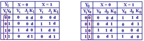
We now derive the input equations for flip-flop 1.
|
Y2Y1Y0 |
X = 0 |
X = 1 |
||||
|
|
Y1 |
J1 |
K1 |
Y1 |
J1 |
K1 |
|
0 0 0 |
0 |
0 |
d |
0 |
0 |
d |
|
0 0 1 |
0 |
0 |
d |
1 |
1 |
d |
|
0 1 1 |
0 |
d |
1 |
1 |
d |
0 |
|
1 0 0 |
0 |
0 |
d |
0 |
0 |
d |
|
1 0 1 |
0 |
0 |
d |
1 |
1 |
d |
The patterns are detected first for X = 0 and X = 1 separately and then combined.
X = 0 X = 1
J1 = 0 J1 = Y0
K1 = 1 K1 = 0 thus J1 = X·Y0 and K1 = X’.
We now derive the input equations for flip-flop 0.
|
Y2Y1Y0 |
X = 0 |
X = 1 |
||||
|
|
Y0 |
J0 |
K0 |
Y0 |
J0 |
K0 |
|
0 0 0 |
0 |
0 |
d |
1 |
1 |
d |
|
0 0 1 |
0 |
d |
1 |
1 |
d |
0 |
|
0 1 1 |
0 |
d |
1 |
1 |
d |
0 |
|
1 0 0 |
0 |
0 |
d |
1 |
1 |
d |
|
1 0 1 |
0 |
d |
1 |
1 |
d |
0 |
The patterns are detected as above
X = 0 X = 1
J0 = 0 J0 = 1
K0 = 1 K0 = 0 thus J0 = X and K0 = X’, as expected.
Step 9 – Summarize the Equations
The purpose of this step is to place all of the equations into one location and facilitate grading by the instructor. Basically we already have all of the answers.
Z = X·Y2·Y0
J2 = X’·Y1 and
J1 = X·Y0 and K1 = X’
J0 = X and K0 = X’
Step 10 – Draw the Circuit
I usually do not ask for this step as it tends to be messy and is always hard to grade.
The figure on the next page has been added to show a typical drawing of this circuit as implemented by JK flip-flops.
Here is the circuit for the 11011 sequence detector as implemented with JK flip-flops.
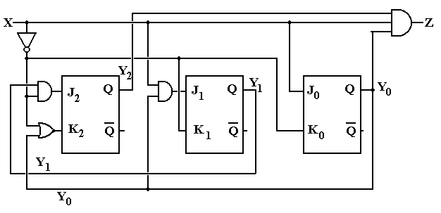
The equations implemented in this design are:
Z = X·Y2·Y0
J2
= X’·Y1
J1 = X·Y0 K1 = X’
J0 = X K0 = X’
Here is the same design implemented with D flip-flops.
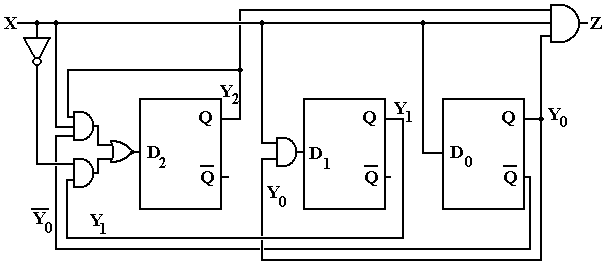
The equations for this design are D2 = X’·Y1 + X·Y2·Y0’
D1 = X ·Y0
D0 = X
More on Overlap – What it is and What it is not
At this point, we need to focus more precisely on the idea of overlap in a sequence detector. For an extended example here, we shall use a 1011 sequence detector.
The next figure shows a partial state diagram for the sequence detector. The final transitions from state D are not specified; this is intentional.
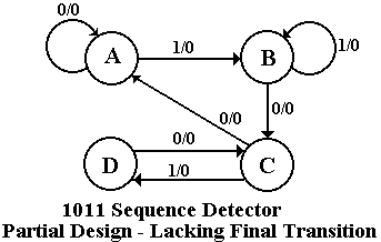 Here
we focus on state C and the X=0 transition coming out of state D. By definition of the system states,
Here
we focus on state C and the X=0 transition coming out of state D. By definition of the system states,
State C – the last two bits were 10
State D – the last three bits were 101.
If the system is in state D and gets a 0 then the last four bits were 1010, not the desired sequence. If the last four bits were 1010, the last two were 10 – go to state C. The design must reuse as many bits as possible.
Note that this decision to go to state C when given a 0 is state D is totally independent of whether or not we are allowing overlap. The question of overlap concerns what to do when the sequence is detected, not what to do when we have input that breaks the sequence.
Just to be complete, we give the state diagrams for the two implementations of the sequence detector – one allowing overlap and one not allowing overlap.
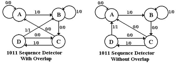
The student should note that the decision on overlap does not affect designs for handling partial results – only what to do when the final 1 in the sequence 1011 is detected.
Solved Problems
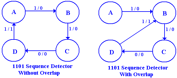
1. Construct a 1101 sequence detector using JK flip-flops.
a) This
is a four state machine. You must label
the states as
A, B, C, and D. Start at state A. Make the following assignments.
A 00 C 10
B 01 D 11
b) Follow
my steps fairly closely. Be sure to
group your answers
at the end of the problem so
that I can find them.
c) The
circuit diagram is optional.
CRITICISM: The problem does not
specify whether or not overlap is allowed.
This is a serious omission, so I shall have to present two solutions and
accept either one.
ANSWER: As requested of you, I shall follow the steps in my method fairly closely.
Step 1 – Derive the State Diagram and
State Table for the Problem
Step 1a Determine the Number of States
This is a four-bit sequence detector, so
the Finite State Machine (FSM) has four states.
As indicated in the assignment, we
label the states as A, B, C, and D.
Step 1b Characterize Each State
State Has Needs For overlap analysis, note the following
A --- 1101
B 1 101 1101 1101 1101
C 11 01 1101 1101
1101
D 110 1 OK No Good No
Good
The
overlap causes a return to state B.
Step 1c Do the Transitions for the Expected
Sequence
Step 1d Insert the Inputs That Break the
Sequence
State A needs a 1 to cause a transition
to state B.
Given a 0 in state A, the FSM remains in state A.
State B has a 1 and needs a 1 to
transition to state C.
If state B gets a 0, the last two bits input are 10 – not a part of the sequence.
Given a 0 in state B, the FSM returns to state A.
State C has the last two bits input as
11 and needs a 0 to transition to state D.
If state C gets a 1, the last three bits input are 111 and the last two input
are 11.
Given a 1 in state C, the FSM remains in state C.
State D has the last three bits input
as 110 and needs a 1 to complete the sequence.
If state D gets a 0, the last four bits input are 1100 – not a part of the
sequence.
Given a 0 in state D, the FSM returns to state A.
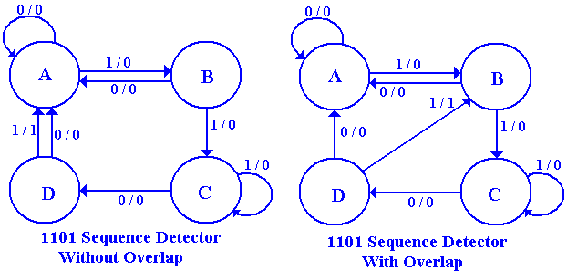
The complete state diagram for the detector is thus the following.
Step 1e Generate the State Table with Output
|
PS |
NS / Z |
|
|
|
X = 0 |
X = 1 |
|
A |
A / 0 |
B / 0 |
|
B |
A / 0 |
C / 0 |
|
C |
D / 0 |
C / 0 |
|
D |
A / 0 |
B / 1 |
|
PS |
NS / Z |
|
|
|
X = 0 |
X = 1 |
|
A |
A / 0 |
B / 0 |
|
B |
A / 0 |
C / 0 |
|
C |
D / 0 |
C / 0 |
|
D |
A / 0 |
A / 1 |
Overlap
Not Allowed With
Overlap
Step 2 – Determine the Number of
Flip-Flops Required
Solve the equation 2P-1 < N £ 2P, for N = 4. It is seen by inspection that P = 2 is the solution of this equation, as 2 < 4 £ 4, or 21 < 4 £ 22. We need two flip-flops.
Step 3 – Assign a Unique P-Bit Binary
Number to Each State
As P = 2,
we are to assign a unique 2-bit number to each state. The assignments specified in the problem
statement are A = 00, B = 01, C = 10, and D = 11. The flip-flops will be labeled
Y1 and Y0, so the state is labeled as Y1Y0.
Step 4 – Generate the Transistion Table with Output
|
PS |
NS / Z |
||
|
|
|
X = 0 |
X = 1 |
|
A |
00 |
00 / 0 |
01 / 0 |
|
B |
01 |
00 / 0 |
10 / 0 |
|
C |
10 |
11 / 0 |
10 / 0 |
|
D |
11 |
00 / 0 |
01 / 1 |
|
PS |
NS / Z |
||
|
|
|
X = 0 |
X = 1 |
|
A |
00 |
00 / 0 |
01 / 0 |
|
B |
01 |
00 / 0 |
10 / 0 |
|
C |
10 |
11 / 0 |
10 / 0 |
|
D |
11 |
00 / 0 |
00 / 1 |
Overlap
Not Allowed With
Overlap
Step 4a – Generate the Output Table and
Output Equation
This is the same for both the overlap and non-overlap case.
|
PS |
Z |
|
|
Y1Y0 |
X = 0 |
X = 1 |
|
00 |
0 |
0 |
|
01 |
0 |
0 |
|
10 |
0 |
0 |
|
11 |
0 |
1 |
The only output occurs when X = 1, Y1 = 1, and Y0 = 1.
The output equation is thus Z = X · Y1 · Y0, a product term.
Step 5 – Separate the Transition Table
into Two Tables, One for Each Flip-Flop
Step 6 – Decide on the Type of Flip-Flops
to Use
The problem specifies that JK flip-flops be used.
|
Q(T) |
Q(T + 1) |
J |
K |
|
0 |
0 |
0 |
d |
|
0 |
1 |
1 |
d |
|
1 |
0 |
d |
1 |
|
1 |
1 |
d |
0 |
The table
at right is the excitation table for
a JK
flip-flop. We shall need to use the
excitation table in order to deduce the inputs to each flip-flop that will make
the circuit behave in the desired manner.
Step 7 – Derive an Input Table for Each
Flip-Flop
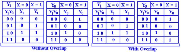
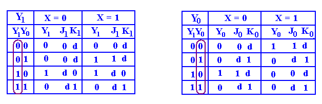
Here we shall do first the no-overlap case and then the overlap case.
Without Overlap
With Overlap
Note that only one entry is different here.
Step 8 – Produce the Input Equations for Each Flip-Flop.
What we are doing here is producing an equation that matches each 0 and 1 in a column. The don’t-care conditions, signified by “d” in the columns, are ignored. We try matching in increasing order of complexity. We must match to variables in the present state column.
1) The first try should
be 0 or 1. If a column has no 1’s in it,
it is matched by 0.
If the column has no 0’s in
it, it is matched by 1.
2) We
next try to match to simple variables or their complements.
3) The
next step is combinations of the variables.
Step 8a – Produce the Equations for the X = 0 and X = 1 Parts of Each
Flip-Flop
Step 8b – Use the “Combine Rule” to Produce
the Equations
Without Overlap
For
X = 0 J1 = 0 and K1 = Y0 For
X = 0 J0 = Y1 and
K0 = 1
For X = 1 J1 = Y0 and K1 = Y0 For X = 1 J0 = Y1’ and K0 = 1
Use the Combine Rule: Expression = X’·(Expression for X = 0) + X·(Expression for X = 1)
J1 = X’·0 + X·Y0
= X·Y0 J0
= X’·Y1
+ X·Y1’
= X Å
Y1
K1 = X’·Y0
+ X·Y0
= Y0 K0
= X’·1
+ X·1
= X’ + X = 1
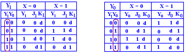
With Overlap
Note that only one entry is different. The Y0 table is different, the Y1 table is the same.
J1 = X·Y0 For X = 0 J0 = Y1 and K0 = 1
K1 = Y0 For
X = 1 J0 = Y1’ and
K0 = Y1’
Using the
Combine Rule for J0 and K0, we get
J0 = X’·Y1
+ X·Y1’
= X Å
Y1
K0 = X’·1
+ X·Y1’
= X’ + X·Y1’
= X’ + Y1’
We now prove the last equality for K0 –
that X’ + X·Y1’
= X’ + Y1’.
Let X = 0. Then LHS = 0’
+ 0·Y1’
= 1 + 0 = 1 and RHS = 0’ + Y1’ = 1 + Y1’ = 1
Let X = 1. Then LHS = 1’ + 1·Y1’ = Y1’
and RHS = 1’ + Y1’ = 0 + Y1’ = Y1’
Step 9 – Summarize the Equations
The output equation is Z = X · Y1 · Y0.
For the case with no
overlap.
J1 = X·Y0 J0 = X Å Y1
K1 = Y0 K0 = 1
For the case with overlap allowed
J1 = X·Y0 J0 = X Å Y1
K1 = Y0 K0 = X’ + Y1’