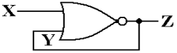
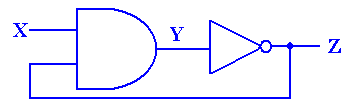
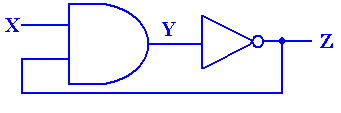
Now consider what happens when X
= 0 in the above circuit. If Y = 0 then
Z = 1, and if
Y = 1 then Z = 0. But the circuit
requires that Y = Z. Were it not for the
gate delay associated with the NOR gate we would have an impossible situation.
We now present the circuit again
and do a detailed timing analysis. We
start with X = 1, which causes Z = 0 and thus Y = 0. But NOR(1, 0) = 0, so we have a stable
circuit. At some later time, the input X
becomes X = 1, and things become interesting.
With X = 0 and Y = 0, the output
Z remains at 0 for one gate delay (approximately ten nanoseconds) and then
becomes 1. Y instantaneously becomes 1
also, as it is connected to Z through a straight wire with a delay of less than
0.001 nanoseconds. With X = 0 and Y = 1,
Z becomes 0 after another gate delay. Y
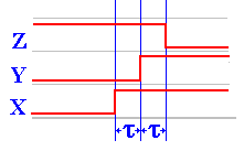
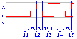
then becomes 0 and Z changes after another gate delay to Z = 1. The whole situation is show in the figure
just above.
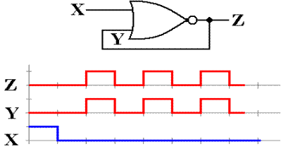
In a moment, we shall turn our
attention to the system clock, which is seen as a regular square wave of the
sort seen for either Y or Z in the above figure. Indeed, this circuit could be used for
generating a standard clock pulse. The
reason that it is not is probably related to lack of uniformity in the gate
delay; measurements for a large number of such circuits might yield gate delays
from 9.9 to 10.1 nanoseconds. Modern
electronic units, including all computers, use a crystal oscillator to generate
clock pulses at a very precise frequency.
Quartz, being piezoelectric, is the most commonly chosen crystal.
Review of Frequency Measurements
At this time, it might be good to review the notation used to speak of
clocks and clock frequencies. The common
unit is a Hertz, named after a physicist who made notable contributions to the
theory of electricity and magnetism. The
unit is abbreviated “Hz”.
An event happens at a frequency
of 1 Hz if it happens once per second.
It happens at a frequency of 1,000 Hz if it happens one thousand times
per second. The frequency of a system clock
is the number of clock pulses generated per second.
|
Frequency
|
Interpretation
|
Pulse Duration
|
|
1 KHz
|
1,000 pulses per second
|
0.001 second = 1 millisecond
|
|
1 MHz
|
1, 000, 000 pulses per second
|
0.000 001 second = 1 microsecond
|
|
1 GHz
|
1, 000, 000, 000 pulses per second
|
0.000 000 001 second = 1 nanosecond
|
Combinational and Sequential
Circuits
We have spent some time considering combinational
circuits. Combinational circuits are the
basis of all digital devices, yet they do not suffice for any but the simplest designs. The one significant weakness of combinational
circuits is that they do not have memory.
In digital devices, memory is based on a feedback mechanism, in which
the output of a combinational circuit is delayed for some amount of time and
then fed back as input to the circuit.
The concept of feedback is familiar
to the small number of us with background in electrical engineering, but most
of us would prefer the functional approach; memory stores data. At this point in our discussions, we shall
just mention that feedback is a daily occurrence, often seen at music
concerts. Think of the situation in
which a microphone is placed too close to one of those big speakers. Any random noise is input to the microphone,
amplified, sounded by the speaker, and fed back into the microphone. This leads to a “run away” feedback.
Before discussing memory devices,
let’s review the difference between the two types of circuits. The table below shows a number of ways to
think about the one and only difference between the two; sequential circuits
have memory and combinational circuits do not.
Combinational Circuits Sequential Circuits
No
Memory Memory
No flip-flops or latches, Flip-flops and
latches may be used
only combinational gates Combinational
gates may be used
No feedback Feedback is allowed
Output for a given set of The order of
input change
inputs is independent of is quite
important and may
order in which these inputs produce significant
differences
were changed, after the in the output,
even after it stabilizes.
output stabilizes.
The following figure shows a way to consider sequential
circuits.
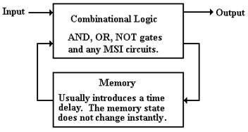
The input is fed into the
combinational logic (AND gates, OR gates, and NOT gates). The output of the combinational logic is fed
into the memory and available as input to the combinational logic after a
specified time delay.
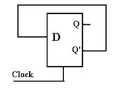
The Idea of a Flip–Flop
Although we have yet to give a
formal definition of a flip–flop, we can now give an intuitive one. A flip–flop is a “bit box”; it stores a
single binary bit. By Q(t), we denote
the state of the flip–flop at the present time, or present tick of the clock;
either Q(t) = 0 or Q(t) = 1. The student
will note that throughout this textbook we make the assumption that all circuit
elements function correctly, so that any binary device is assumed to have only
two states.
A flip–flop must have an output;
this is called either Q or Q(t). This
output indicates the current state of the flip–flop, and as such is either a
binary 0 or a binary 1. We shall see
that, as a result of the way in which they are constructed, all flip–flops also
output , the complement of the current state. Each flip–flop also has, as input, signals
that specify how the next state, Q(t + 1), is to relate to the present state,
Q(t).
, the complement of the current state. Each flip–flop also has, as input, signals
that specify how the next state, Q(t + 1), is to relate to the present state,
Q(t).
Every flip–flop also has an
input derived from the system clock, which allows it to function as a
synchronous circuit. It also has
connections to power and ground.
The Clock
The most
fundamental characteristic of synchronous sequential circuits is a system
clock. This is an electronic circuit
that produces a repetitive train of logic 1 and logic 0 at a regular rate,
called the clock frequency. Most computer systems have a number of
clocks, usually operating at related frequencies; for example – 2 GHz, 1GHz,
500MHz, and 125MHz. The inverse of the
clock frequency is the clock cycle time. As an example, we consider a clock with a
frequency of 2 GHz (2·109 Hertz).
The cycle time is 1.0 / (2·109) seconds, or
0.5·10–9
seconds = 0.500 nanoseconds = 500 picoseconds.
Synchronous sequential
circuits are sequential circuits that use a clock input to order
events. Asynchronous sequential circuits
do not use a common clock and, as hinted at above, are much harder to design
and test. As we shall focus only on
synchronous circuits, we immediately launch a discussion of the clock.
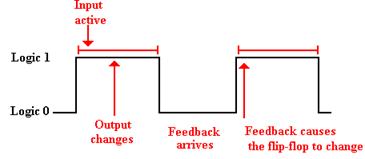
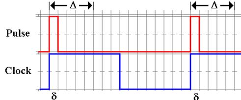
The following figure illustrates
some of the terms commonly used for a clock.
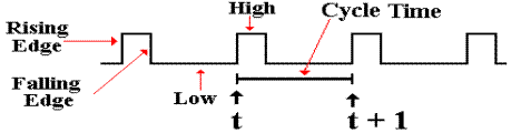
The clock input is very
important to the concept of a sequential circuit. At each “tick” of the clock the output of a
sequential circuit is determined by its input and by its state. We now provide a common definition of a “clock
tick” – it occurs at the rising edge of each pulse. We use t to represent the time at a clock
tick and (t + 1) to denote the time at the next clock tick – the difference
between the two is the clock cycle time.
Suppose a 2 GHz clock, which corresponds to a clock cycle time of 0.5
nanosecond. Strictly speaking, we should
label our timings in nanoseconds: 1.0, 1.5. 2.0. 2.5, etc. The convention is just to count the ticks,
referring to the present clock pulse as occurring at time t and the next one at time (t
+ 1).
Diversion: What the Clock Signals Really Look Like
The figure above represents the
clock as a well-behaved square wave.
This is far from the actual truth, as can be seen by examining the clock
pulses with sufficient resolution. The
following figure presents three views of the clock pulse train produced by a
typical clock: a realistic physical view and two notations for approximating
the clock.
In reality, the clock pulse is
not square, but rises and falls exponentially.
For those with mathematical interest, the clock falls in a function of
the form e –ax and rises with the form of the function 1 – e –bx,
where a
»
b. Use of this precise form does not gain us
anything and leads to significant difficulties, so that unless we are
troubleshooting at a very low level, we approximate the clock by either a
trapezoidal wave or a square wave.
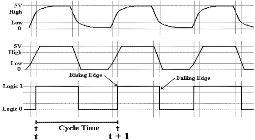
The
trapezoidal wave form is used when it is important to emphasize the fact that
the clock does take some time to rise and fall.
One sees this form of clock representation often when examining timing
diagrams for system buses. The square
wave is a further abstraction of the real electrical form of the wave;
fortunately it is quite often an adequate representation. The square wave representation remains at
logic 0 until the real electrical clock crosses the threshold for logic high
(about 2.5 volts) at which time the square wave jumps to logic 1. The square wave remains at logic 1 until the
real electrical clock signal crosses the threshold for logic low (about 0.8
volts) at which time the square wave goes to logic 0.
In this
course, we shall never have to worry ourselves with the actual electrical
representation of a clock and seldom shall worry about the trapezoidal representation. The main point of this diversion is to
explain clearly that some logical models are quite useful, even when they do
not represent the physical reality with complete accuracy.
The
“bottom line” to this argument is that we use the simplest model that will show
what we need to see in considering a problem.
Here, we find that the only real requirement for a clock is to
differentiate the “present state” from the “next state”; a square wave clock
will do.
The NOR Gate and
an SR Latch
We now begin our investigation
of flip–flops. We begin with the SR flip–flop, which is the simplest. In order to understand an SR flip–flop, we
must first discuss the SR latch. In
order to understand the SR latch, we must review the properties of the NOR
gate.
The NOR gate, as depicted in the
following diagram, is logically equivalent to an OR gate followed by a NOT
gate. In reality, it is faster than its
equivalent; a typical NOR has a gate delay of 10 nanoseconds; the gate delays total
23.5 nanoseconds for the OR/NOT circuit.
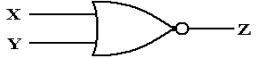
As we have seen previously, the
truth table for the NOR gate can be written as follows.
|
Y
|
X
|
Z
|
|
0
|
0
|
1
|
|
0
|
1
|
0
|
|
1
|
0
|
0
|
|
1
|
1
|
0
|
To support our next discussion, it will prove useful to reduce
this table to two equations.
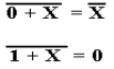
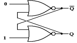
Given these equations, we consider
the following circuit with cross–coupled NOR gates. We stipulate that the two inputs to the
circuit are both held at logical zero.
At this point, we do not know the value of Q or care about it; just that
the two outputs are complements.
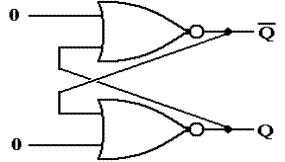
Rewriting the top equation with
X first as Q and then with X as  , we have these equations.
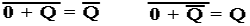
An examination of this circuit
shows it to be stable. The top NOR gate
has as input 0 and Q; its output is . The bottom
NOR gate has as input 0 and ; its output is Q.
The output of each gate is precisely the previous input to the other
gate, so nothing changes.
As we shall see, things become
interesting when one of the inputs becomes 1.
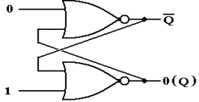
We now imagine the circuit in
one of two logically consistent states (where Q and are not equal)
and change the top input to logic 1. At
first, the situation is little changed, as the NOR gates have not yet reacted
to the new input.
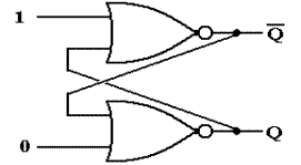
Note that the input to the top device is now 1 and Q (which
is either 0 or 1). The inputs to the
bottom NOR gate have yet to change and will not until after one gate
delay. Recall that

for each of the two possible
values of Q. After one gate delay, the
output of the top NOR gate has changed to 0, but that the output of the bottom NOR
gate has yet to respond to its new input, which has just arrived.
After the second gate delay, the
output of the bottom NOR gate becomes 1, as
NOR(0, 0) = 1. The input to the top NOR
gate might change, but its output will not change, as NOR(1, 1) = 0. The circuit is now stable.
Let’s review what happened and
clarify some of the labeling. At the
beginning, the device had some state, denoted by Q in the diagram. It will be called Q(t) when we have a clocked
device, but for now it is just “Q”.
Changing the value of the top input to 1 and leaving the bottom input at
0 induces some changes that take two gate delays to complete. The circuit is now stable, with a value of Q
= 1. This is the “new value of Q” as
opposed to the “old value of Q”, which might have been 1, but just as easily
could have been 0.
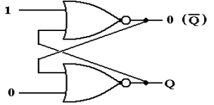
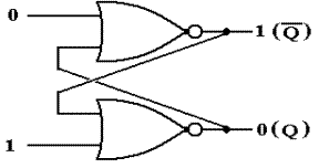
We now go back to the circuit in
one of two logically consistent states (where Q and are not equal)
and change the bottom input to logic 1, leaving the top input as 0. At first, the situation is little changed, as
the NOR gates have not yet reacted to the new input.
Note that the input to the bottom device is now 1 and (which is
either 0 or 1). The inputs to the bottom
NOR gate have yet to change and will not until after one gate delay. Now:

for
each of the two possible values of . After one
gate delay, the output of the bottom
NOR gate has changed to 0, but that the output of the top NOR gate has yet to
respond to its new input, which has just arrived.
After the second gate delay, the
output of the top NOR gate becomes 1, as NOR(0, 0) = 1. The input to the bottom NOR gate might
change, but its output will not change, as
NOR(1, 1) = 0. The circuit is now
stable.
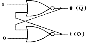
We note in passing the fourth possible input
combination. Recall that

for any possible value of
X. Suppose that both the top and bottom
inputs are set to 1. The only possible
outputs are Q = 0 and = 0. This is obviously invalid.
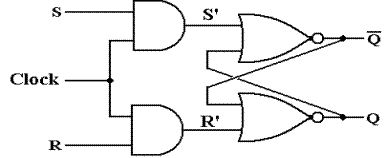
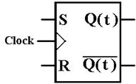
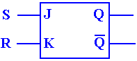
What we have here is called an SR Latch. The name SR comes from “Set Reset”. The general diagram for the SR latch is as
below, where the S input is the “Set input” and the R input is the “Reset
input”. When a latch is set, its value
becomes 1. When a latch is reset, its
value becomes 0. In this figure, the
value is denoted by Q and its complement by .
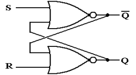
Supposing that the old value of the SR latch is denoted
by Q, we have the following truth table to describe the response to the
input. Such a table is called a “characteristic table”.
|
S
|
R
|
New Value
|
|
0
|
0
|
Q
|
|
0
|
1
|
0
|
|
1
|
0
|
1
|
|
1
|
1
|
Invalid
|
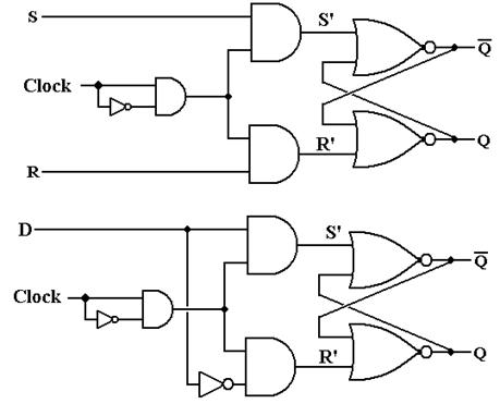
The Clocked SR Latch
The circuit above is interesting (at least to the author of this textbook),
but somewhat troublesome. The problem is
that it will change state any time the input changes. Normal design practice, especially in
synchronous circuits, demands that the change take place only during certain
phases of the system clock. The circuit
to accommodate this design constraint is called either a “clocked SR latch” or
a “level triggered SR flip–flop”. The
circuit diagram for a clocked SR latch is shown in the following figure.
This circuit is just an SR latch
with the input passed through a pair of AND gates. When the input Clock = 0, each of S’ and R’
are 0 without regard to the values of S and R.
The latch does not change state, but keeps its current value. When the input Clock (also called “Enable”,
“Strobe”, or just “Wake Up and Look at the Input”) is 1, the SR latch responds
to the input values of S and R as discussed above.
The Clocked D Latch
The clocked D latch is a specialization of the clocked SR latch. The term “D” in “D Latch” and later in “D
Flip–Flop” indicates “Data” and shows that the device stores data. When the clock input is 1, the device will
store its input. The D latch can be
constructed from an SR latch as indicated in the following circuit diagram.
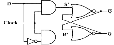
Note that when Clock = 0, both
S’ = 0 and R’ = 0, without regard to the value of D. When Clock = 1, then each of S’ and R’ depend
on D; S’ = D and R’ =  . This leads to
the following characteristic table for the latch.
. This leads to
the following characteristic table for the latch.
|
Clock
|
D
|
S’
|
R’
|
New Value
|
|
0
|
0
|
0
|
0
|
Q
|
|
0
|
1
|
0
|
0
|
Q
|
|
1
|
0
|
0
|
1
|
0
|
|
1
|
1
|
1
|
0
|
1
|
In a clocked latch, the ability to respond to input is
connected to an external signal, called “Clock”. This signal is based on the system clock, but
might be modified as needed. The next
figure shows a circuit that loads dependent on a signal called “Load”.
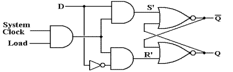
The signal called “Load” is
obviously generated by a control circuit that is synchronous with the system
clock. The timing diagram for this
signal might be as follows.
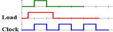
The SR latch accepts input if
and only if both Clock = 1 and Load = 1.
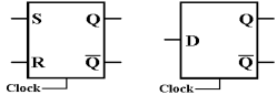
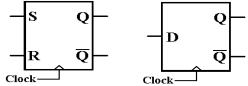
Notation for Latches and
Flip–Flops
When showing either latches or flip–flops as circuit elements, it is
undesirable to show the “internals” of the device. We need a simple schematic for latches and
flip–flops that shows what we need to see and no more. Here is the standard symbology
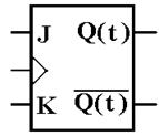
for each of SR and D circuits, both flip–flops and latches.
The notation adopted is a simple
box notation, with the outputs and inputs shown. The difference between the symbol for a latch
and that for a flip–flop lies in the handling of the clock input. A flip–flop, also called an “edge triggered
flip–flop” is shown with a small triangle attached to the clock input. For SR and D devices, we have the following
symbols.
Here are the symbols for SR and D latches.
Here are the symbols for SR and D flip–flops, which we have
not yet defined.
Note the small triangles on the clock input; this says “edge triggered”.
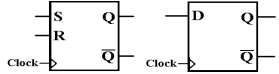
One should note that the more
common symbols for flip–flops show the clock input coming
in “from the side” as shown in the next figure.
Clocked Latches and
Flip–Flops
The two most common synchronous sequential devices are clocked latches and
flip–flops. In a few pages, we shall see
that a flip–flop is essentially a clocked latch that has been modified. For the moment, we shall just note that both
clocked latches and flip–flops change state in response to the input, sampled
at a fixed part of the system clock cycle.
The standard way to describe
each of these devices uses a characteristic
table, which defines the state at the next clock tick in terms of the input
and the state at the present clock tick.
Recalling our notation that “t” stands for the current clock tick and “t
+ 1” stands for the next clock tick, we say that we determine Q(t + 1) in terms
of Q(t) and the input.
One should note that clocked
latches and flip–flops share characteristic tables, so that the characteristic
table for an SR latch would also be that for an SR flip–flop and the
characteristic table for a D latch would also describe a D flip–flop. The difference between clocked latches and
flip–flops lies in how the device reacts to the clock.
The Feedback Problem with
Clocked Latches.
The problem with clocked latches is that they respond to the input whenever
their clock input is set at logic one.
For the above example, this occurs whenever both the System Clock and
the Load signal are set to logic 1. As
good design practice calls for Load to go to logic 1 before the rising edge of
the system clock and remain at 1 past the falling edge, the latch will respond
to input during a time interval equal to at least one half of the clock cycle
time.
Consider a circuit in which
there is feedback to the circuit.
As a concrete example of the problem, we consider an otherwise
silly circuit that has the potential for displaying the timing issues very
clearly. In this circuit, we have D =  , with the intention of having Q(t + 1) = ; the circuit oscillates. As with any sufficiently simple example,
there are obvious ways to get this done more easily; that is not the
point. The circuit that we consider is
shown below.
, with the intention of having Q(t + 1) = ; the circuit oscillates. As with any sufficiently simple example,
there are obvious ways to get this done more easily; that is not the
point. The circuit that we consider is
shown below.
The key issue here is the propagation delay for the line
feeding the D input; the interval between the time that Q’ changes and the time
at which D changes. Were that interval
greater than one half of the system clock period, the circuit might function as
expected.
Here is the timing diagram for what we intend to happen.
Note that the feedback cannot
loop back to the D input either too early or too late. It is rarely the case that the input arrives
too late; this is a problem that is easy to solve. However, it is very likely that the feedback
will arrive too early. This will cause
instabilities.
Consider what might happen when
the interval for propagation is much less than the clock period. In this next example, we make the reasonable
assumption that the D input changes 0.5 gate delays (for the clocked D latch)
after the output Q changes, and that the clock period is somewhat greater than
10 gate delays.
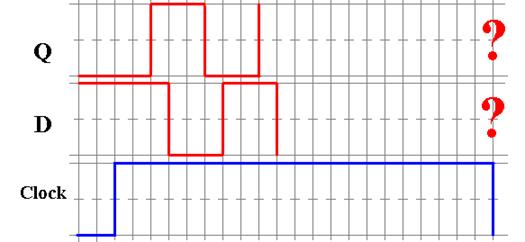
At the beginning of this time
trace, we have a consistent situation. Q
= 0 and D = = 1. The clock then goes high and stays high for a
number of gate delays. We have the
following sequence of events, with the times measured in multiple of gate
delays.
T = 0.0 The
clock goes high and the D latch responds to its input.
T = 1.0 The value of Q changes in response to the new value of D.
T = 1.5 The value of D changes, as it is equal to
.
T = 2.5 The value of Q changes again.
T = 3.0 The value of D changes again
T = ?? The clock goes low and the value of Q is unpredictable.
Please
note that the unpredictability of the output of the flip–flop is due to the
uncertain relation between the clock time and the sum of the gate delay times
for the flip–flop. In general, the clock
cycle time will be known to a very high accuracy (1 part in a million, or
better), but the gate delay times are only approximations, quoted as averages.
The problem lies in the fact
that, even with the use of a clocked latch, we have lost control of the
feedback loop. This has lead to
instability. We now consider the first
of two possible solutions to managing the feedback loop; this is called a
“Master/Slave” flip–flop.
We have two problems with the
nomenclature. The first is that the
device is not a flip–flop in the current sense of the word. It is just a clocked latch that is called a
flip–flop.
The second issue we have with
the nomenclature is the term “Master/Slave”.
To be blunt, the term is not politically correct and we do like to be
politically correct whenever possible.
Some time ago, the IEEE (Institute
of Electronic and
Electrical Engineers) sponsored a contest through its magazine “Computer” to
find an alternative name for this device.
All reasonable answers were published in the journal; all were
ridiculous and some quite suggestive of practices best left unmentioned in
polite company. The bottom line is that
we are stuck with the term if we discuss latches; with real flip–flops the
problem goes away.
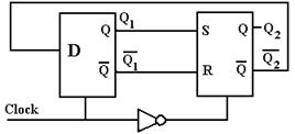
The D Master–Slave Latch
Basically, a Master–Slave device is fabricated from two clocked latches by
joining them, as follows. Note that the
second latch is often an SR latch, as it is simpler.
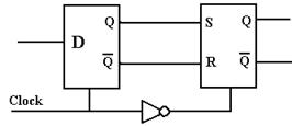
Here we note that a correctly
functioning D latch will never allow S = 1 and R = 1 to be input to the second
latch, so the SR undefined input does not arise. The important feature of this arrangement is
the NOT gate in the clock line. When the
D latch accepts input, the SR latch cannot; and when the SR latch accepts
input, the D latch cannot.
To see the functioning of this
combination, let us again examine the above silly circuit, this time implemented
with a Master/Slave D latch. First we
see the circuit, then the timings.
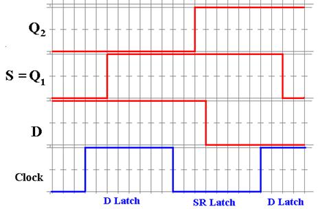
At the start, we have Q2
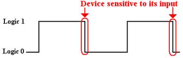
= 0 and D = 1, with the D latch not sensitive to its input. When the clock becomes high, the D latch
becomes sensitive to its input, and Q1 changes after a time to allow
for the gate delays in the latch. Now
the SR latch has S = 1 and R = 0 (not shown), but it is not yet sensitive to
these inputs. When the clock goes low, the
SR latch accepts its input and after its gate delays changes its output. Almost immediately, the value of D changes,
but the D latch is no longer sensitive to its input. The D input takes effect at the next clock
pulse.
What the Master/Slave latch
accomplishes is to control the feedback loop by causing the output to be
delayed until the time at which the master latch is no longer sensitive to its
input. When the clock next goes high,
the master latch responds and a new cycle begins.
Level Triggering and Edge Triggering
The feedback problem that was
addressed by the Master/Slave latch was due to the fact that the master latch
was sensitive to its input for a full half of the clock cycle. We now examine another solution to this problem,
one that makes the latch sensitive for a much shorter time. We begin by reviewing the concept of level
triggering, then introduce the idea called “edge
triggering”, and conclude by designing a mechanism that allows for edge
triggering.
To review, a clocked latch is
sensitive to its input during one half of the clock cycle, usually when the
clock is “high” (at logic level 1), but not necessarily so.
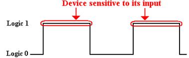
By definition, an edge triggered
flip–flop is sensitive only during an edge of the clock pulse. We can have positive edge triggering, as shown just below.
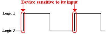
We can also have negative
edge triggering, as shown just below.
By way of giving the precise
definition of a flip–flop, we quote Andrew S. Tanenbaum.
For emphasis, we will repeat the
difference between a flip–flop and a latch.
A flip–flop is edge triggered, whereas a latch is level triggered. Be warned, however, that in the literature
these terms are often confused. Many
authors
use “flip–flop” when they are referring to a latch, and vice versa.
( Andrew
S. Tanenbaum, Structured Computer Organization,
Fifth Edition,
Pearson/Prentice–Hall, 2006. ISBN 0 – 13 – 148521 – 0. Page 162 )
Flip–Flops
By definition, a flip–flop is an edge–triggered latch. We must now show how to achieve edge
triggering. In essence, what we shall do
is take a level triggered latch and give it a clock pulse with a very short
positive (logical 1) phase.
The key component of an
edge–triggered flip–flop is a pulse generator that we studied in a previous
chapter. This could be based on the gate
delay of a NOT gate. More modern devices
likely use a different circuit so as to generate a shorter pulse.
Now that we have a method to
generate a short pulse, we can build an edge–triggered device. The following is a diagram of the components
of two typical edge–triggered flip–flops.
The top one is a SR flip–flop and the bottom one is a D flip–flop.
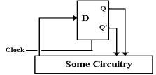
Feedback for Flip–Flops
Part of our motivation for master/slave latches, discussed above, was the
problem of feedback. We now pose the
same problem in our consideration of flip–flops. In order to avoid the simple and silly
example used the first time, we shall examine the general case.
Here is the circuit for
consideration. We postulate a total of
gate delays (including that of the D flip–flop) to be the time interval
signified by D. Thus at time D after the D latch is
first sensitive to its input, the circuitry has output a new value to become
D. But the flip–flop is activated by a
short pulse, of time length d.
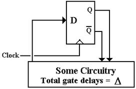
The timing diagram below shows
the interruption of the uncontrolled feedback loop. By the time that the output of the circuitry
has changed, the D flip–flop is no longer sensitive to input. The input will not become effective until the
beginning of the next clock cycle.
How can one insure that the relative
timings of two circuits, the D flip–flop and the rest of the CPU circuitry,
operate with the correct timings? This
is one of the issues of central importance in the design of a CPU; since we
have stumbled into it, let’s talk about it.
To be more precise, define two
total gate delays: DMIN and DMAX. DMIN is the
total time delay for the fastest CPU operation and DMAX.
the delay for the slowest. We must have
DMIN
> d,
or the circuit would occasionally display uncontrolled feedback. Conservatively, we might say DMIN
³
1.5·d. The next criterion is a bit more difficult to
state precisely, but it might be stated something like T ³ 1.5·DMAX,
where T denotes the clock period. What
we say here is that the clock period must be long enough for the CPU output to
“settle”. Note, however, that a value of
T much larger than DMAX is just wasted time.
Put another way, the value of DMAX
determines the fastest clock that can reasonably be applied to the CPU. A good part of the art of CPU design is based
on this issue. When we study the RISC
(Reduced Instruction Set Computer) movement, we shall see that one of the
issues was to remove the more complex instructions, thus reducing DMAX
and allowing for a faster clock. There
is a trade–off here that we shall explore in later chapters.
To be honest, the sum of CPU
gate delays is not always the limiting factor in the clock speed. Some recent CPUs have been designed with a
“hot clock” that is hot in both ways. It
is very fast, being of the order of 4 to 5 GHz.
It is also hot in the literal sense, in that the CPU, operating at that
clock rate, emits so much heat that it overheats itself. The art of CPU design is always bumping up
against those messy laws of physics.
The SR Flip–Flop
We have completely defined the SR flip–flop, based on the idea of an SR
latch. While we could just leave the
topic and proceed, it is appropriate at this time to review the subject and
state, in one place, what the student is expected to know. We begin with a depiction of the SR flip–flop
that will be used in all future discussions.
At this point we are no longer
interested in the internal construction of the flip–flop, but on its
operational characteristics. These are
given in the characteristic table.
|
S
|
R
|
Q(t + 1)
|
|
0
|
0
|
Q(t)
|
|
0
|
1
|
0
|
|
1
|
0
|
1
|
|
1
|
1
|
ERROR
|
We next address an issue that commonly arises in the use of
flip–flops in circuit design. We have a
number of scenarios. For each, we know
Q(t) and what Q(t + 1) should be. The question is how to achieve that
change. For example, if Q(t) = 0 and we
want Q(t + 1) = 0, we have two choices: either S = 0 and R = 0, or S = 0 and R
= 1. The first option, keeps the state
unchanged at 0; the second forces it to 0.
As S = 0 is sufficient to do this without regard to the value of R, we
say that the input is S = 0 and R = d; the d standing for “don’t care”.
On the other hand, if Q(t) = 0
and Q(t + 1) = 1, only S = 1 and R = 0 will do.
This is the only combination that will give a next state of 1 when the
present state is 0.
If we have Q(t) = 1 and want Q(t
+ 1) = 0, then our choice is simple: S = 0 and R = 1.
If we have Q(t) = 1 and want Q(t
+ 1) = 1, then we can choose either S = 0 and R = 0, or
S = 1 and R = 0. This is denoted as S =
d and R = 0.
The above discussions lead to
the excitation table for the SR flip–flop.
|
Q(t)
|
Q(t + 1)
|
S
|
R
|
|
0
|
0
|
0
|
d
|
|
0
|
1
|
1
|
0
|
|
1
|
0
|
0
|
1
|
|
1
|
1
|
d
|
0
|
The JK Flip–Flop: Enhancing the SR Flip–Flop
Recall the characteristic table of the SR flip–flop. We repeat the table here for emphasis.
|
S
|
R
|
Q(t + 1)
|
|
0
|
0
|
Q(t)
|
|
0
|
1
|
0
|
|
1
|
0
|
1
|
|
1
|
1
|
ERROR
|
The
theoretician examining this table would note two facts immediately.
1. The
input S = 1 and R = 1 is disallowed; we would like to do something with it.
2. The
values for Q(t + 1) are three of the possible four Boolean functions of 1
variable.
Considering Q as a Boolean
variable, we now show that there are exactly four Boolean functions of this
Boolean variable. These are f(Q) = 0, f(Q) = 1, f(Q) = Q, and f(Q) =  . We do this by
showing the truth table for each of these functions and noting that there are
only four different ways to put 0’s and 1’s into the two row entries for a
function..
. We do this by
showing the truth table for each of these functions and noting that there are
only four different ways to put 0’s and 1’s into the two row entries for a
function..
|
Q
|
0
|
Q
|
|
1
|
|
0
|
0
|
0
|
1
|
1
|
|
1
|
0
|
1
|
0
|
1
|
Table: The Four Boolean Functions of
Boolean Variable Q
Given this, our enhanced SR
flip–flop would have Q(t + 1) = (t) as one possible output. For maximal compatibility with the existing
SR, we would want to leave the existing valid inputs alone and just make good
use of the invalid one. What we get is a
JK flip–flop.
Recalling that an SR flip–flop
is so called because it is a Set–Reset device, we may ask for the
meaning of JK. One is tempted to make up
some story related to names in German, but the basic answer is that “I don’t
know”. In any case, we present the
characteristic table for the JK flip–flop and then ask how one might modify an
SR flip to achieve that goal.
Here is the desired
characteristic table.
|
J
|
K
|
Q(t + 1)
|
|
0
|
0
|
Q(t)
|
|
0
|
1
|
0
|
|
1
|
0
|
1
|
|
1
|
1
|
(t)
|
Viewing
this as a modification of the SR flip–flop, we ask how to generate each of S
and R from the inputs J and K under the following constraints;
1. Except
when J = 1 and K = 1, we want to have S = J and R = K.
Under these circumstances, the
behavior is identical.
2. When
J = 1, K = 1, and Q = 0, we want S = 1 and R = 0. This makes Q(t + 1) = 1.
3. When
J = 1, K = 1, and Q = 1, we want S = 0 and R = 1. This makes Q(t + 1) = 0.
When in
doubt about how to create a circuit, we make a truth table. The inputs to the truth table are J, K, and Q
(the present state). The outputs are S
and R.
|
Row
|
Q
|
J
|
K
|
|
S
|
R
|
|
0
|
0
|
0
|
0
|
|
0
|
0
|
|
1
|
0
|
0
|
1
|
|
0
|
1
|
|
2
|
0
|
1
|
0
|
|
1
|
0
|
|
3
|
0
|
1
|
1
|
|
1
|
0
|
|
4
|
1
|
0
|
0
|
|
0
|
0
|
|
5
|
1
|
0
|
1
|
|
0
|
1
|
|
6
|
1
|
1
|
0
|
|
1
|
0
|
|
7
|
1
|
1
|
1
|
|
0
|
1
|
We have two patterns that almost work: S
= J· and R = K·Q. Let’s examine each case.
S = J· produces the
expected result for all rows except row 6.
In that row we have
Q = 1, J = 1, and K = 0. We want Q(t +
1) to be 1. But S = 0 and R = 0 will cause
Q(t + 1) = Q(t) = 1, exactly what we want.
So this simple formula causes no trouble.
R = K·Q
produces the expected result for all rows except row 1. In that row we have
Q = 0, J = 0, and K = 1. We want Q(t +
1) to be 0. But S = 0 and R = 0 will cause
Q(t + 1) = Q(t) = 0, exactly what we want.
So again we have no trouble.
Here is the
basic detailed circuit for the JK flip–flop.
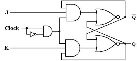
We now give
the standard representation of the JK flip–flop as will be used in future
discussions. Again, note the triangle
symbol on the clock input, indicating edge triggering.
We have
already presented the characteristic
table for the JK flip–flop. Here it
is again.
|
J
|
K
|
Q(t + 1)
|
|
0
|
0
|
Q(t)
|
|
0
|
1
|
0
|
|
1
|
0
|
1
|
|
1
|
1
|
(t)
|
We now create the excitation table for
the JK.
If Q(t) = 0
and Q(t + 1) is to be 0, we can use either J = 0 and K = 0, or J = 0 and K = 1.
If Q(t) = 0
and Q(t + 1) is to be 1, we can use either J = 1 and K = 0, or J = 1 and K = 1.
Note that this is a new option, not
available for an SR flip–flop.
If Q(t) = 1
and Q(t + 1) is to be 0, we can use either J = 0 and K = 1, or J = 1 and K = 1.
Note that this also is a new option,
not available for an SR flip–flop.
If Q(t) =
1 and Q(t + 1) is to be 1, we can use either J = 0 and K = 0, or J = 1 and K =
0.
This gives
the excitation table for the JK
flip–flop.
|
Q(t)
|
Q(t + 1)
|
J
|
K
|
|
0
|
0
|
0
|
d
|
|
0
|
1
|
1
|
d
|
|
1
|
0
|
d
|
1
|
|
1
|
1
|
d
|
0
|
The D Flip–Flop
We have already examined the D latch. The
input is labeled “D” for “Data”. The D
flip–flop has a characteristic table identical to that of a D latch.
The device is so simple that it does not
require an excitation equation. We just
use an excitation equation, which simply states “Give it what you want”.
D = Q(t + 1)
The T Flip–Flop
This is the fourth and last of the major types of flip–flops. The input to this flip–flop is labeled “T”
for toggle. When T = 0, the state
remains the same. When T = 1, the
flip–flop changes state. This gives rise
to the following characteristic table.
|
T
|
Q(t
+ 1)
|
|
0
|
Q(t)
|
|
1
|
(t)
|
The excitation
table for this flip–flop is almost obvious.
|
Q(t)
|
Q(t
+ 1)
|
T
|
|
0
|
0
|
0
|
|
0
|
1
|
1
|
|
1
|
0
|
1
|
|
1
|
1
|
0
|
This gives rise to an excitation
equation.
T = Q(t) Å Q(t + 1)
The JK As a General Flip–Flop
We now take notice that the JK can be configured to function as any of
the other 3 flip–flop types. In this, it
is the most general type of flip–flop.
The JK As a D Flip–Flop
To convert a JK to a D flip–flop, connect the inputs as follows.
If D = 0,
then J = 0, K = 1, and Q(t + 1) = 0, If
D = 1, then J = 1, K = 0, and Q(t + 1) = 1.
The JK As A T Flip–Flop
To convert a JK to a T flip–flop, connect the inputs as follows.
If T = 0,
then J = 0, K = 0, and Q(t + 1) = Q(t).
If T = 1, then J = 1, K = 1, and Q(t + 1) = (t)
Registers
A register is a storage device capable of holding binary
data. It is best viewed as a collection
of flip-flops, usually D flip-flops. To
store N bits, a register must have N flip-flops, one for each bit to be
stored. We show a design for a four-bit
register with a synchronous LOAD.
In this example, the 4-bit register is implemented by four D
flip-flops.
Note the input CLK comes from an AND gate that puts out the
logical AND of the system clock (Clock) and the LOAD signal. When LOAD is 0, the flip-flops are cut off
from the input and do not change state in response to the input. The design calls for LOAD to be 1 for almost
one clock pulse, so that the system clock and LOAD are both high for 1/2 clock
cycle. At this time, the register is
loaded.
The figure at right shows a short-hand notation used when
drawing registers that contain a number of flip-flops identically configured.
It should be obvious that the figure represents a 4-bit
register.
Definition: A register
file is a collection of registers that is considered logically as a unit,
and each of which can be individually addressed. For example, one modern computer has thirty–two
general purpose registers in the CPU, denoted in its assembly language as
%R0 through %R31. This collection of
registers is considered a register file.
Admittedly, the terminology is rather old, and might be obsolete, but it
works for this author.
Consider a register file containing two 4-bit
registers. The registers will be named
R0 and R1, and selected by a one-bit control signal, called R; R = 0 selects R0
and R = 1 selects R1. Note that the
figure was drawn before this author changed the notation to %R0 and %R1.
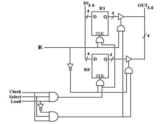
Analysis of this diagram shows how it works. Begin with the interaction of the Load and
Select signal. If Select = 0, neither
register will be active. If Select = 1,
the selected register will be loaded if Load = 1 and read (contents copied out)
if Load = 0.
There may be other options for
controlling such a collection of registers, but all such require two control
signals as there are three options for a register
1) Do
nothing – save the current contents
2) Copy
the input to the register and possibly change its contents
3) Copy
the register contents to the output.
Also save the contents.
We now present a register file
structure that will be of importance in our design of a model computer. To conform to the design used later in the
book, this figure should show eight
32–bit registers for a total of 224 flip-flops (8 · 32 = 256 and 7 · 32 =
224, we explain this apparent contradiction a bit later), which would present
difficulties in drawing. For the sake of
simplicity and legibility, we present a file of four two–bit registers, with a
two-bit input bus on the left and a two-bit output bus on the right.
The signal Bus ® Reg
causes the selected register to be loaded from the bus at left.
The signal Reg ® Bus causes the
contents of the selected register to be copied out.
Something Is Missing
Recall that an N–bit register
requires N flip–flops; hence a two-bit register requires two
flip-flops and a register file of four two–bit registers requires eight
flip-flops. Yet our design above has
only six flip-flops. The observant
student will notice that there seems to be no register %R0. We seem to have three fully functioning
two-bit registers that we could name as %R1, %R2, and %R3.
To understand the functioning
of the register file above, let us focus on a single bit and both its
flip-flops and circuitry for reading and writing those flip-flops. We first consider the output circuitry,
controlled by a 4-to-1 multiplexer and an enabled-high tri-state buffer.
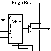
The two bits entering the
multiplexer from the bottom are the control bits for the multiplexer and
represent the 2-bit binary code for the register to be selected. If the signal Reg ® Bus is active, then
the output of the multiplexer is placed on the output bus. It is easy to see that if the binary codes
are 01, 10, or 11 that the contents of the flip-flop for %R1, %R2, or %R3 are
output to the bus. But if the code is
00, the output bus is connected to ground, effectively placing a 0 on the
output bus.
We now consider the input
circuitry. Note that the inputs of every
flip-flop associated with this bit are directly connected to the appropriate
bit-line of the input bus and that the register to receive the input is
activated by its CLOCK input. Here is
the circuitry for producing the CLOCK input to the flip-flops associated with
the register that is selected for input.
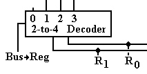 If
the signal Bus ®
Reg is not active, the decoder is not enabled and
all of its output lines are inactive.
Thus, no register is selected for input.
If Bus ®
Reg = 1, then the flip-flops for that register
receive a CLOCK pulse and accept the input from the appropriate bit-line of the
input bus. This works well for register
codes 01, 10, and 11.
If
the signal Bus ®
Reg is not active, the decoder is not enabled and
all of its output lines are inactive.
Thus, no register is selected for input.
If Bus ®
Reg = 1, then the flip-flops for that register
receive a CLOCK pulse and accept the input from the appropriate bit-line of the
input bus. This works well for register
codes 01, 10, and 11.
But what about register-select
code 00? If R1R0 =
00 and Bus ®
Reg = 1, output 0 of the decoder is active but is
not connected to anything. To be blunt,
no register is loaded.
The Phantom Register %R0
Let us review what happens when
the register select codes are R1R0 = 00, indicating a
selection of register %R0.
If Reg ® Bus is asserted, the
number 0 is copied out to the output bus.
If Bus ® Reg
is asserted and Reg ® Bus
is not asserted, nothing happens.
What we have here is (%R0) º 0,
that is register 0 is a constant register holding the constant value 0. Registers that hold constant values are not
implemented with flip-flops, but with connections to ground (logic 0) and to
voltage (logic 1). The use of a register
with its select code equal to decimal 0 greatly facilitates the design of the
control unit of the CPU.
As we design the control unit,
we shall add other constant registers that are not part of the general purpose
register set. Unlike %R0, these will not
be accessed by the assembly language, but are used by the control unit. The most likely candidate is the constant 1,
depicted in binary as 0000
0000 0000 0000 0000 0000 0001 – bit 0 is connected to positive voltage
(logic 1) and bits 1 through 31 connected to ground (logic 0).
Why Have a Register for Zero?
The above discussion suggests a valid question with an
entirely valid answer. To jump ahead, we
postulate a three-bus design with the buses labeled as B1, B2, and B3. Suppose I want to transfer the contents of B1
to B3, in RTL (Register Transfer Language) B3 ¬ (B1). One way would be to set B2 to all zeroes and
have B3 ¬
(B1) + (B2); thus implementing the algebraic equation Y = X + 0 rather than the
equivalent Y = X. The reason that we
must set the contents of B2 to 0 in order for this to work is that otherwise
the contents of B2 would be undefined and might take any possible value as
dictated by electrical noise.
As we develop the logic of the control unit for the CPU, we
shall see why it is simpler to issue the control signal B3 ¬ (B1)
+ (B2) with (B2) º
0, rather than the apparently simpler control signal B3 ¬ (B1). It all comes down to making a simpler and
faster CPU.
More on Register Files
We now consider the idea of a register file as used later in
the design of our model CPU.
This is a collection of eight registers, labeled %R0 through %R7, each a 32-bit
register.
As 8 = 23 registers, there are three register select lines, labeled
R2R1R0.
Our CPU design will call for three CPU buses, labeled B1,
B2, and B3. Buses B1 and B2 will be used
as input to the ALU (Arithmetic-Logic Unit, the part that does the math), and
bus B3 will be used as output of the ALU. Thus the register file will support output to
two buses (B1 and B2) and input from a single bus (B3).
The register file for this design has
32 input lines, labeled IN31
- 0
Two sets
of32 output lines, each labeled OUT31
- 0
3 register
select lines, labeled R2 – 0 or alternatively R2R1R0.
Reg ® B1, Reg ® B2,
B3 ®
Reg, and Clock signals
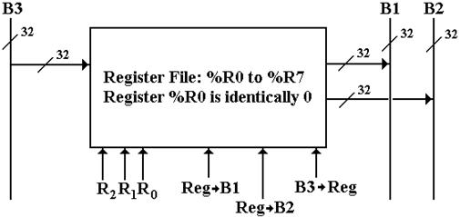
Figure: The Register File for Our Computer and Its Data Buses
Registers: Some Miscellaneous
Remarks
We now consider a few designs for registers to be
constructed from flip-flops. Since the
issues to be considered do not depend on the number of bits to be stored in the
register, we consider a 1–bit register.
Consider the following design.
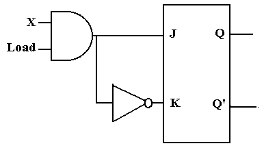 The
input to this circuit is X. When Load =
1, the output of the AND gate is X and the input to the flip-flop is J = X and
K = X’, as desired.
The
input to this circuit is X. When Load =
1, the output of the AND gate is X and the input to the flip-flop is J = X and
K = X’, as desired.
The problem arises when the register is to keep its contents
and Load = 0. The output of the AND gate
is 0 and the input to the flip-flop is J = 0 and K = 1. The flip-flop is cleared; the auto-forget
option.
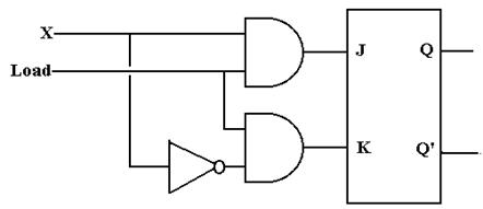 The
correct circuit is shown at the right.
When Load = 1, the input to the flip-flop is J = X and K = X’, as
desired.
The
correct circuit is shown at the right.
When Load = 1, the input to the flip-flop is J = X and K = X’, as
desired.
When Load = 0, the input to the flip-flop is J = 0 and K =
0, and the flip-flop maintains its current state.
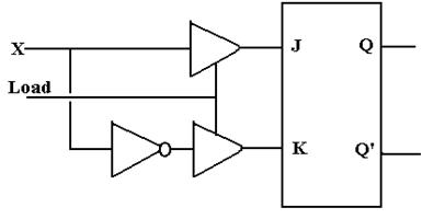 We
now consider the use of tri-state buffers to control input. When Load = 1, the circuit operates as
desired. But consider Load = 0. Both tri-states are disabled, giving a high-impedance
output, which is interpreted as logic 1 by the flip-flop. When Load = 0, we have J = 1 and K = 1 and
that is trouble.
We
now consider the use of tri-state buffers to control input. When Load = 1, the circuit operates as
desired. But consider Load = 0. Both tri-states are disabled, giving a high-impedance
output, which is interpreted as logic 1 by the flip-flop. When Load = 0, we have J = 1 and K = 1 and
that is trouble.
The bottom line: tri-states cannot be used on input.
Shift Registers
We now consider the following circuit built from four D
flip-flops.
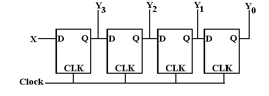
Before each clock pulse, D3 = X and DK
= QK+1 for 0 £ K £ 2. If QK(T)
is the state before the clock pulse and QK(T + 1) is the state after
the clock pulse, then the situation after the clock pulse is given by Q3(T
+ 1) = X and QK(T + 1) = QK+1(T) for 0 £ K £
2. The input bits in X are thus seen to
be shifted across the four flip-flops, hence the name.
Since we don’t like to draw too many flip-flops, we have a
symbol for shift registers.
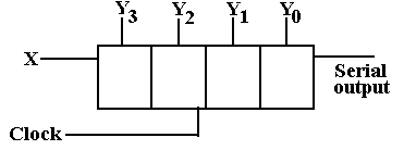 The
shift register has both serial
The
shift register has both serial
input and parallel input.
The
parallel input is through the lines
labeled by the Y’s, a notation we
have normally used for output
only. Two common
modes are
parallel in / serial out and
serial in / parallel out.
Shift registers are of great use for handling serial Input/Output devices, which transmit data one bit at a
time. Consider the case of a character
‘B’ coming in on a serial input line.
The ASCII character code for ‘B’ is 42 hexadecimal, so the binary input
is 01000010. This input is passed into
an 8-bit shift register. After 8 clock
cycles, the state of the shift register is
Y7 = 0, Y6 = 1, Y5 = 0, Y4 = 0, Y3
= 0, Y2 = 0, Y1 = 1, and Y0 = 0. This is then transferred into the CPU as
parallel data. For output, the character
code is transferred in parallel into the shift register and then shifted out
one bit at a time, producing the serial bit stream.
More detailed study of serial I/O indicates that there are a
few more details to be considered.
We now consider schemes for data transfer between shift
registers. We first consider in detail a
design shown in some textbooks. We then
show a preferred design.
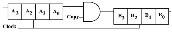
This circuit, copied from another textbook, has many
problems. A complete analysis of the
circuit depends on the input to the flip-flop labeled A3. If the input is undefined, it will be
interpreted as a 1. If it is logic 0,
then zeroes will be shifted in. For our
analysis, we shall assume that the input is specified by a proper source, thus
avoiding these problems.
Suppose that the Copy control signal goes to 1 at T = 0,
when the contents of registers A and B are X3X2X1X0
and Y3Y2Y1Y0, respectively. We analyze this circuit and find it has many
problems. The A register is cleared
rather than copied.
|
Time
|
Copy
|
A3
|
A2
|
A1
|
A0
|
B3
|
B2
|
B1
|
B0
|
|
0
|
1
|
X3
|
X2
|
X1
|
X0
|
Y3
|
Y2
|
Y1
|
Y0
|
|
1
|
1
|
0
|
X3
|
X2
|
X1
|
X0
|
Y3
|
Y2
|
Y1
|
|
2
|
1
|
0
|
0
|
X3
|
X2
|
X1
|
X0
|
Y3
|
Y2
|
|
3
|
1
|
0
|
0
|
0
|
X3
|
X2
|
X1
|
X0
|
Y3
|
|
4
|
0
|
0
|
0
|
0
|
0
|
X3
|
X2
|
X1
|
X0
|
|
5
|
0
|
0
|
0
|
0
|
0
|
0
|
X3
|
X2
|
X1
|
|
6
|
0
|
0
|
0
|
0
|
0
|
0
|
0
|
X3
|
X2
|
|
7
|
0
|
0
|
0
|
0
|
0
|
0
|
0
|
0
|
X3
|
|
8
|
0
|
0
|
0
|
0
|
0
|
0
|
0
|
0
|
0
|
The problem with this circuit is that the system clock is
sent directly into the clock input of the shift registers, so they shift
continuously. The input to A (presumed
0) is shifted first into A and then into B.
At the end, all information is lost.
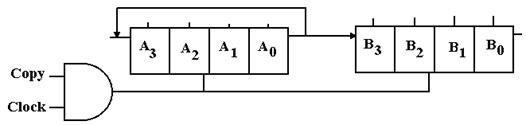
The correct shift register uses the Copy control signal to
pass the clock signal to the shift registers or keep it from getting to
them. It also re-circulates the A
register to prevent loss.
Solved Problems
PROBLEM
1. A Set-Dominate flip-flop acts like the SR flip-flop except that S
= R = 1 sets the flip-flop.
Show the characteristic table and
the state table for a set-dominate SR flip-flop.
ANSWER:
The state
table for the flip-flop may be written as follows.
|
S
|
R
|
Q(T+1)
|
Comments
|
|
0
|
0
|
Q(T)
|
Same
as SR
|
|
0
|
1
|
0
|
Same
as SR
|
|
1
|
0
|
1
|
Same
as SR
|
|
1
|
1
|
1
|
This
is the only difference.
|
There
is another form of the state table that is occasionally used. The instructor prefers state tables in the
form above, but presents an equivalent state table below. Those students who prefer the form of the
following table should feel free to use it.
|
PS
\ Input
|
S
= 0, R = 0
|
S
= 0, R = 1
|
S
= 1, R = 0
|
S
= 1, R = 1
|
|
Q(T)
= 0
|
0
|
0
|
1
|
1
|
|
Q(T)
= 1
|
1
|
0
|
1
|
1
|
Again,
note that only in column for S = 1 and R = 1 do we see a difference between
this
flip-flop and the standard SR flip-flop.
The
excitation table for this flip-flop
presents difficulties as the notation we use is not adequate to expression of
the input for one case. Let’s start with
a partial solution.
Q(T) Q(T + 1) S R
0 0 0 d S
= 0, R = 0 makes Q(T + 1) = Q(T) = 0
S
= 0, R = 1 makes Q(T + 1) = 0
0 1 1 d S
= 1, R = 0 makes Q(T + 1) = 1
S
= 1, R = 1 makes Q(T + 1) = 1
1 0 0 1 S
= 0, R = 1 makes Q(T + 1) = 0
But
look at Q(T) = 1 and Q(T + 1) = 1.
S = 0 and R = 0 makes Q(T + 1) = Q(T) = 1
S = 1 and R = 0 makes Q(T + 1) = 1
S = 1 and R = 1 makes Q(T + 1) = 1
The
only input that does not get Q(T + 1) = 1 for Q(T) = 1 is S = 0 and R = 1.
Note
that the solution for the last line of the excitation table should be “anything
but
S = 0 and R = 1”. We have not developed
a notation for this concept. Here is one
answer.
|
Q(T)
|
Q(T + 1)
|
S R
|
|
0
|
0
|
0 d
|
|
0
|
1
|
1 d
|
|
1
|
0
|
0 1
|
|
1
|
1
|
0 0
1 d
|
S
= 0, R = 0 and S = 1, R = 0 can combine to S = d, R = 0
S
= 1, R = 0 and S = 1, R = 1 can combine to S = 1, R = d.
|
Q(T)
|
Q(T +
1)
|
S R
|
|
0
|
0
|
0 d
|
|
0
|
1
|
1 d
|
|
1
|
0
|
0 1
|
|
1
|
1
|
d 0
1 1
|
Here
is another table that represents the same information.
Note
that d 0 can stand for either 0 0 or 1 0, so again we have covered the three
possible answers 0 0, 1 0, or 1 1.
|
Q(T)
|
Q(T + 1)
|
S R
|
|
0
|
0
|
0 d
|
|
0
|
1
|
1 d
|
|
1
|
0
|
0 1
|
|
1
|
1
|
d 0
1 d
|
Another
possible solution would be to combine the two above as shown at left. Note the following.
d
0 expands to 0 0 and 1 0
1
d expands to 1 0 and 1 1.
We
have 1 0 covered twice, but that is quite valid.
COMMENTS: Again, the problem is that our notation does
not cover the situation required for this design: we have no way to express
“anything but 0 1”. This does not excuse
the student from realizing this problem and writing the answer correctly.
One
student put the following
|
Q(T)
|
Q(T
+ 1)
|
S R
|
|
1
|
1
|
d d
|
Note
that this allows S = 0 and R = 1, which will cause Q(T + 1) = 0.
The
whole purpose of assigning this problem is for the student to work out how to
represent this last line in the excitation table. The set dominate flip-flop is not very
interesting apart from being fodder for this homework assignment.
SOLVED PROBLEMs
1. Analyze the
behavior of the circuit labeled “Dubious Circuit of Unknown Use” as found
earlier in this chapter. Assume that the
circuit begins with X = 0 and trace the behavior from the time that X = 1 is
asserted. Assume a propagation delay of t
for each gate. The circuit is
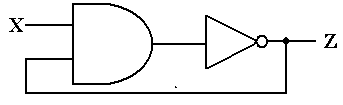
ANSWER:
This is a bit of an unusual problem, not the sort that I
would assign for this course. I could
not resist showing you the solution, once I had worked it out.
In order to analyze this circuit, we must first label the
output of the AND gate. This gives rise
to the next version of the figure, with the AND gate output labeled as Y.
Now consider what happens when X = 0. Recalling that 0·Z = 0, we see that Y = 0
without regard to the value of Z and Z = 1 remains stable. To pursue the analysis further, we must first
look at a slightly different circuit – one without the feedback.
When X = 0, Y = 0, and Z = 1. The following diagram shows what happens just
after the moment in time when X becomes 1.
 At
time t after X becomes 1, Y becomes 0. At time t after Y becomes 0, Z becomes 1. Thus Z becomes 1 at a time 2t
after X becomes 0. It is this delay of 2t
that allows the circuit to display its behavior.
At
time t after X becomes 1, Y becomes 0. At time t after Y becomes 0, Z becomes 1. Thus Z becomes 1 at a time 2t
after X becomes 0. It is this delay of 2t
that allows the circuit to display its behavior.
We now analyze the behavior of the full circuit, reproduced
here from the previous page.
The behavior of the circuit is shown in the following
diagram. As noted above, when X = 0, we
have Y = 0 (without regard to the value of Z) and Z = 1. This is a stable situation. Things change just after X becomes 1.
1. At T1, X
becomes 1. Since Z = 1, we have X·Z = 1·1 =
1. But Y remains at 0.
2. At T1 + t, Y
becomes 1. Z remains at 1.
3. At T2 = T1 + 2t,
Z becomes 0. Thus the input to the AND
gate are X = 1, Z = 0.
4. At T2 + t, Y
becomes 0. Z remains at 0.
5. At T3 = T2 + 2t,
Z becomes 1. Thus the input to the AND
gate are X = 1, Z = 1.
6. At T3 + t, Y
becomes 1. Z remains at 1.
7. At T4 = T3 + 2t,
Z becomes 0. Thus the input to the AND
gate are X = 1, Z = 0.
And so forth.
2. Use a JK flip-flop
to implement an SR flip-flop.
ANSWER
 This
is a trick question. A JK flip-flop is
just like an SR, except that the SR cannot take S = 1 and R = 1. Just hook up the JK with J = S and K = R and
never give it both
This
is a trick question. A JK flip-flop is
just like an SR, except that the SR cannot take S = 1 and R = 1. Just hook up the JK with J = S and K = R and
never give it both
J = 1 and K = 1. This
is a really silly questioin.
3. Use an SR
flip-flop and some basic gates (AND, OR, or NOT) to realize a JK flip-flop.
ANSWER
Unlike the previous question, this is a real one. We must work with the characteristic table of
the JK flip-flop and the excitation table of the SR flip-flop. We use the characteristic table of the JK to
specify the desired behavior and the excitation table for the SR flip-flop to
determine the input to that flip-flop necessary to make it behave that way.
|
J
|
K
|
Q(T+1)
|
|
0
|
0
|
Q(T)
|
|
0
|
1
|
0
|
|
1
|
0
|
1
|
|
1
|
1
|
Q’(T)
|
The characteristic table of the JK flip-flop is shown at
right.
The main difference between the JK flip-flop and the SR
flip-flop is that the JK allows an input J = 1 and K = 1, which causes the
state of the flip-flop to change; Q(T+1) = Q’(T).
|
Q(T)
|
Q(T+1)
|
S
|
R
|
|
0
|
0
|
0
|
d
|
|
0
|
1
|
1
|
0
|
|
1
|
0
|
0
|
1
|
|
1
|
1
|
d
|
0
|
The excitation table of the SR flip-flop is shown at
left. Note that the transitions between
states 0 and 1 are somewhat more constrained that allowed for the JK.
We now rewrite the characteristic table of the JK,
explicitly allowing for Q(T) = 0 and
Q(T) = 1. We then append the appropriate
columns of the SR excitation table.
|
J
|
K
|
Q(T)
|
Q(T+1)
|
S
|
R
|
|
0
|
0
|
0
|
0
|
0
|
d
|
|
0
|
0
|
1
|
1
|
d
|
0
|
|
0
|
1
|
0
|
0
|
0
|
d
|
|
0
|
1
|
1
|
0
|
0
|
1
|
|
1
|
0
|
0
|
1
|
1
|
0
|
|
1
|
0
|
1
|
1
|
d
|
0
|
|
1
|
1
|
0
|
1
|
1
|
0
|
|
1
|
1
|
1
|
0
|
0
|
1
|
We must now make S and R functions of J, K, and
Q(T). Note that we cannot use Q(T+1), as
this is not a crystal ball circuit.
When J = 0, S matches 0.
When J = 1, S matches Q’(T). So S = J·Q’(T).
When K = 0, R matches 0.
When K = 1, R matches Q(T). So R = K·Q(T).
The circuit is shown just below.
There are two ways to produce Boolean expressions for S and
R. These notes will focus on the more
intuitive and informal process of pattern matching, which we now try to
explain.
Consider first the determination of the expression for
S. It must be given as an expression
based only on J, K, and Q(T). Let’s
repeat the table with these four columns only.
|
J
|
K
|
Q(T)
|
S
|
|
0
|
0
|
0
|
0
|
|
0
|
0
|
1
|
d
|
|
0
|
1
|
0
|
0
|
|
0
|
1
|
1
|
0
|
|
1
|
0
|
0
|
1
|
|
1
|
0
|
1
|
d
|
|
1
|
1
|
0
|
1
|
|
1
|
1
|
1
|
0
|
The goal of any pattern matching is to find an expression
that matches the 0’s and 1’s exactly and ignores the “don’t cares”. In the top half of the table, for which J =
0, note that the number 1 does not appear in the column for S. This causes us to select one of two choices
for S; either S = 0 or S = J.
In the bottom half of the table, for which J = 1, we find
both O’s and 1’s in the column for S.
Thus S = 1 is not a match. We
then attempt to find a simple pattern that matches S. Note that it does not match either K or Q(T),
so we must move to more complex.
The key to this match is to note that whenever S = 1, Q(T) =
0 and whenever S = 0, Q(T) = 1. The best
match for the J = 1 half of the table is Q’(T).
Thus the best match for the whole table is S = J·Q’(T). Other matches include the following canonical
form expression.
S = J · K’ · Q’(T) + J · K · Q’(T), which simplifies to the same thing, and
S = J’ ·
K’ ·
Q(T) + J ·
K’ ·
Q’(T) + J ·
K’ ·
Q(T) + J ·
K ·
Q’(T), which is silly.
|
J
|
K
|
Q(T)
|
R
|
|
0
|
0
|
0
|
d
|
|
0
|
0
|
1
|
0
|
|
1
|
0
|
0
|
0
|
|
1
|
0
|
1
|
0
|
|
0
|
1
|
0
|
d
|
|
0
|
1
|
1
|
1
|
|
1
|
1
|
0
|
0
|
|
1
|
1
|
1
|
1
|
To see the best match for the Boolean expression for R, we
have rearranged the table so that all the rows for K = 0 come first. This facilitates seeing the match based on
the value of K.
For K = 0, we again see that R = 0 is a good match, as the
column for R has no 1’s in the top half of this rearranged table.
For K = 1, we see that Q(T) = 0 whenever R = 0 and Q(T) = 1
whenever R = 1; we do not care about a match for R = d.
Thus the best match for K = 1 is R = Q(T), and the best match
for the whole table is R = K·Q(T). Again,
other matches are possible, but most other candidates are overly complex or
just plain silly.
We have now arrived at a set of solutions for the problem.
S = J·Q’(T)
R = K·Q(T)
The only thing left to do is draw the diagram (as shown on
the previous page).
A bit later we shall return to a discussion of methods for
matching Boolean expressions to columns of 0’s, 1’s, and “don’t cares”.
4. A set-dominate
flip-flop is similar to an SR flip-flop except that input S = 1, R = 1 sets the
flip-flop; Q(T + 1) = 1, in stead of being an error
condition. Use one JK flip-flop, and basic gates (AND, OR, NOT) as needed to implement
a set-dominate flip-flop; in other words, build a circuit that acts like a
set-dominate flip-flop.
ANSWER:
The
only issue here is again what to do with the input
S = 1, R = 1. If S = 0, we want J = 0
and K = R. Thus
If
S = 1, then we force K = 0.
The
following table illustrates.
|
S
|
R
|
J = S
|
K = S’·R
|
Q(T+1)
|
|
0
|
0
|
0
|
0
|
0
|
|
0
|
1
|
0
|
1
|
0
|
|
1
|
0
|
1
|
0
|
1
|
|
1
|
1
|
1
|
0
|
1
|
5 The following diagram is a modified SR
flip–flop. Use a truth table and the characteristic
table of an SR flip–flop to determine its characteristic table for inputs X, Y
and Z.
ANSWER: First,
note the characteristic table for an SR flip–flop.
|
S
|
R
|
Q(t + 1)
|
|
0
|
0
|
Q(t)
|
|
0
|
1
|
0
|
|
1
|
0
|
1
|
|
1
|
1
|
Error
|
The important equations, deduced from the diagram above, are
as follows:
S = X·Y’ R =
Y·Z
|
X
|
Y
|
Z
|
S
|
R
|
Q(t + 1)
|
|
0
|
0
|
0
|
0
|
0
|
Q(t)
|
|
0
|
0
|
1
|
0
|
0
|
Q(t)
|
|
0
|
1
|
0
|
0
|
0
|
Q(t)
|
|
0
|
1
|
1
|
0
|
1
|
0
|
|
1
|
0
|
0
|
1
|
0
|
1
|
|
1
|
0
|
1
|
1
|
0
|
1
|
|
1
|
1
|
0
|
0
|
0
|
Q(t)
|
|
1
|
1
|
1
|
0
|
1
|
0
|
Appendix:
The Flip–Flop Tables
The SR Flip–Flop
Characteristic Table
|
S
|
R
|
Q(t + 1)
|
|
0
|
0
|
Q(t)
|
|
0
|
1
|
0
|
|
1
|
0
|
1
|
|
1
|
1
|
ERROR
|
Excitation Table
|
Q(t)
|
Q(t + 1)
|
S
|
R
|
|
0
|
0
|
0
|
d
|
|
0
|
1
|
1
|
0
|
|
1
|
0
|
0
|
1
|
|
1
|
1
|
d
|
0
|
The JK Flip–Flop
Characteristic Table
|
J
|
K
|
Q(t + 1)
|
|
0
|
0
|
Q(t)
|
|
0
|
1
|
0
|
|
1
|
0
|
1
|
|
1
|
1
|
(t)
|
Excitation Table
|
Q(t)
|
Q(t + 1)
|
J
|
K
|
|
0
|
0
|
0
|
d
|
|
0
|
1
|
1
|
d
|
|
1
|
0
|
d
|
1
|
|
1
|
1
|
d
|
0
|
The D Flip–Flop
Characteristic Table
Excitation Equation
D
= Q(t + 1)
The T Flip–Flop
Characteristic Table
|
T
|
Q(t
+ 1)
|
|
0
|
Q(t)
|
|
1
|
(t)
|
Excitation Table
|
Q(t)
|
Q(t
+ 1)
|
T
|
|
0
|
0
|
0
|
|
0
|
1
|
1
|
|
1
|
0
|
1
|
|
1
|
1
|
0
|
Excitation Equation
T = Q(t) Å Q(t + 1)