The Electronic Numerical Integrator and Calculator (ENIAC)
The next significant
development in computing machines took place at Moore School of Engineering at
the
At the time the ENIAC was proposed, it was well understood that such a machine could be built. The problem was the same as noted by Zuse and his assistants – how to create a large machine using the fragile vacuum tubes of the day. The ENIAC, as finally built, had over 18,000 vacuum tubes. Without special design precautions, such a complex electronic machine would not have remained functional for any significant time interval, let alone perform any useful work.
The steps taken by Eckert to solve the tube reliability problem are described in a paper “Classic Machines: Technology, Implementation, and Economics” in [R11]
“J. Presper
Eckert solved the tube reliability problem with a number of techniques:
· Tube failures were bimodal, with more
failures near the start of operation as
well as after many hours and less
during the middle operating hours. In
order to achieve better
reliability, he used tubes that had already been
burnt-in [powered up and left to
run for a short time], and had not suffered
from ‘infant mortality’ [had not
burned out when first turned on].
· The machine was not turned off at night
because power cycling [turning the
power off and on] was a source of
increased failures.
· Components were run at only half of their
rated capacity, reducing the
stress and degradation of the tubes
and significantly increasing their
operating lifetime.
· Binary circuits were used, so tubes that
were becoming weak or leaky
would not cause an immediate
failure, as they would in an analog computer.
· The machine was built from circuit modules
whose failure was easy to
ascertain and that could be quickly
replaced with identical modules.”
“As a result of this excellent engineering, ENIAC was able to run for as long as a day or two without a failure! ENIAC was capable of 5,000 operations per second. It took up 2,400 cubic feet [about 70 cubic meters] of circuitry, weighed 30 tons, and consumed 140kW of power.”
While the ENIAC lacked what we would call memory, it did have twenty ten-digit accumulators used to store intermediate results. Each of the ten digits in an accumulator was stored in a shift register of ten flip-flops (for a total of 100 flip-flops per register). According to our reference, a 10–digit accumulator required 550 vacuum tubes, so that the register file by itself required 11,000 vacuum tubes. A bit of arithmetic will show that a 10–digit integer requires 34 bits to represent. Roughly speaking, each accumulator held four 8–bit bytes.
It is this arrangement of the accumulators that might give rise to some confusion. In its instruction architecture, the ENIAC was a decimal machine and not a binary machine; each number being stored as a collection of digits rather than in binary form. As noted above, the ENIAC did use binary devices to store those digits, probably coded with BCD code, and thus gained reliability.
The next figure shows a module for a single digit in a decimal accumulator. Although this circuit was not taken from the ENIAC, it is sufficiently compatible with the technology used in the ENIAC that it might have been taken from that machine.
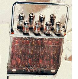
Single Digit from a Burroughs 205
Accumulator, circa 1954.
Source:
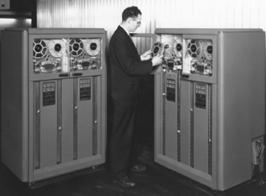
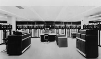
The ENIAC was physically a very large machine as shown by the pictures below.
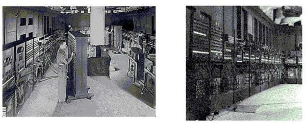
Figure: Two Pictures of the ENIAC
Source: R34
There are several ways to describe the size of the ENIAC. The pictures above, showing an Army private standing at an instrument rack is one. Other pictures include two women programming the ENIAC (using plug cables) or four women, each of whom is holding the circuit to store a single digit in a progression of technologies.
Miss Patsy Simmers, holding an ENIAC board (Operational
in Fall 1945)
Mrs. Gail TAylor, holding an EDVAC board (Delivered in August 1949)
Mrs. Milly Beck, holding an ORDVAC board (Operational in March 1952)
Mrs. Norma Stec, holding a BRLESC-I board (Delivered in May 1961)
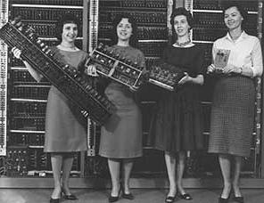
Figure: Four Women With Register Circuits
It is interesting to note that in 1997,
as a part of the 50th anniversary of the ENIAC, a group of students
at the
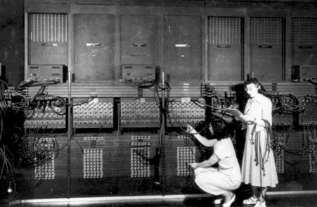
Figure: Two women programming the ENIAC
(Miss Gloria Ruth Gorden on the left and
Mrs. Ester Gertson on the right)
Some Reminiscences about the ENIAC
The following is taken from an interview with J. Presper Eckert, one of the designers of the ENIAC. It was published in the trade journal, Computerworld, on February 20, 2006.
“In the early 1940’s, J. Presper Eckert was
the designer and chief engineer building ENIAC, the first general-purpose
all-electronic computer (see story, page 18).
It was a huge undertaking; ENIAC was the largest electronic device that
had ever been built. So why did Eckert –
on a tight schedule and with a limited staff – take time out to feed electrical
wire to mice?
Because he knew that ENIAC’s hundreds of miles of wiring would be chewed by the
rodents. So he used a cageful of mice to
taste-test wire samples. The wire whose
insulation the mice chewed on least was the stuff Eckert’s team used to wire up
the ENIAC. It was an elegant solution to
an unavoidable problem.”
In the same issue, an earlier interview with Mr. Eckert was recalled.
“In our 1989 interview, I asked ENIAC
co-inventor J. Presper Eckert to recall the zaniest thing he did while
developing the historic computer. His
reply:
‘The mouse cage was pretty funny. We
knew mice would eat the insulation off the wires, so we got samples of all the
wires that were available and put them in a cage with a bunch of mice to see
which insulation they did not like. We
used only wire that passed the mouse test’.”
The Electronic Discrete Variable Automatic Calculator
(EDVAC)
The ENIAC, as a result of its quick production in response to war applications, suffered from a number of shortcomings. The most obvious shortcoming is that it had no random access memory. As it had no place to store a program, it was not a stored–program computer.
The EDVAC, first proposed in 1945 and made operational in 1951, was the first true stored program computer in that it had a memory that could be used to store the program. In this sense, the EDVAC was the earliest design that we would call a computer. This design arose from the experience gained on the ENIAC and was proposed in a report “First Draft of a Report on the EDVAC” written in June 1945 by J. Presper Eckert, John Mauchly, and John von Neumann. The report was distributed citing only von Neumann as the author, so that it has only been recently that Eckert and Mauchly have been recognized as coauthors. In the meantime, the name “von Neumann machine” has become synonymous with “stored program computer” as if von Neumann had created the idea all by himself.
Unlike modern computers, the EDVAC and EDSAC (described below) used bit serial arithmetic. This choice was driven by the memory technology available at the time; it was a serial memory based on mercury acoustic delay lines; each bit of a word had to be either read or written sequentially. To access a given word (44 bits) on its memory, the EDVAC had to wait on the given word to circulate to the memory reader and then read it out, one bit at a time. This memory held 1,024 44–bit words, about 5.5 kilobytes.
The EDVAC had almost 6,000 vacuum tubes and 12,000 solid–state diodes. The CPU addition time was 864 microseconds; the multiplication time 2.9 milliseconds. On average, the EDVAC had a mean time between failures of eight hours and ran 20 hours a day.
The goals of the EDVAC, as quoted from the report, were as follows. Note the use of the word “organs” for what we would now call “components” or “circuits”. [R 37]
“1. Since the device is primarily a computer it will have to perform the elementary operations of arithmetic most frequently. Therefore, it should contain specialized organs for just these operations, i.e., addition, subtraction, multiplication, and division.”
“2. The logical control of the device (i.e., proper sequencing of its operations) can best be carried out by a central control organ.”
“3. A device which is to carry out long and complicated sequences of operation must have a considerable memory capacity.”
“4. The device must have organs to transfer information from the outside recording medium of the device into the central arithmetic part and central control part, and the memory. These organs form its input.”
“5. The device must have organs to transfer information from the central arithmetic part and central control part, and the memory into the outside recording medium. These organs form its output.”
At this point the main challenge in the development of stored program computers is the availability of technologies suitable for creation of the memory. The vacuum tubes available at the time could have been used to create modest-sized memories, but the memory would have been too expensive and not reliable. Consider an 8KB memory – 8,192 bytes of 8 bits each, corresponding to 65,536 bits. A vacuum tube flip-flop implementation of such a memory would have required one vacuum tube per bit, for a total of 65,536 vacuum tubes.
While the terms here are anachronistic, the problem was very real for that time.
Given the above calculation, we see that the big research issue for computer science in the late 1940’s and early 1950’s was the development of inexpensive and reliable memory elements. Early attempts included electrostatic memories and various types of acoustic delay lines (such as memory delay lines).
The Electronic Delay Storage Automatic Calculator
(EDSAC)
While the EDVAC stands as
the first design for a stored program computer, the first such computer
actually built was the EDSAC by Maurice Wilkes of
In building the EDSAC, the first problem that Wilkes attacked was that of devising a suitable memory unit. By early 1947, he had designed and built the first working mercury acoustic delay memory (see the following figure). It consisted of 16 steel tubes, each capable of storing 32 words of 17 bits each (16 bits plus a sign) for a total of 512 words. The delay lines were bit-serial memories, so the EDSAC had a bit-serial design. The reader is invited to note that the EDSAC was a very large computer, but typical of the size for its time.
The next two figures
illustrate the EDSAC I computer, as built at
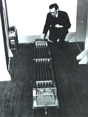
Figure: Maurice Wilkes and a Set of 16
mercury delay lines for the EDSAC [R 38]
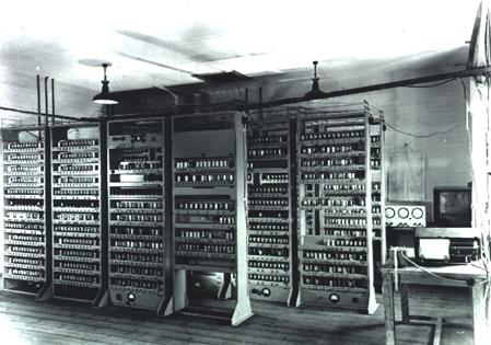
Figure: The EDSAC I [R39]
Note that the computer was built large, with components on racks, so that technicians could have easy access to the electronics when doing routine maintenance.
The design of the EDSAC was somewhat conservative for the time, as Wilkes wanted to create a machine that he could actually program. As a result, the machine cycle time was two microseconds (500 kHz clock rate), slower by a factor of two than other machines being designed at the time. The project pioneered a number of design issues, including the first use of a subroutine call instruction that saved the return address and the use of a linking loader. The subroutine call instruction was named the Wheeler jump, after David J. Wheeler who invented it while working as a graduate student [R11, page 3]. Another of Wheeler’s innovations was the relocating program loader.
Magnetic Core Memory
The reader will note that most discussions of the “computer generations” focus on the technology used to implement the CPU (Central Processing Unit). Here, we shall depart from this “CPU–centric view” and discuss early developments in memory technology. We shall begin this section by presenting a number of the early technologies and end it with what your author considers to be the last significant contribution of the first generation – the magnetic core memory. This technology was introduced with the Whirlwind computer, designed and built at MIT in the late 1940’s and early 1950’s.
The
reader will recall that the ENIAC did not have any memory, but just used twenty
10–digit accumulators. For this reason,
it was not a stored program computer, as it had no memory in which to store the
program. To see the reason for this, let
us perform a thought experiment and design a 4 kilobyte (4,096 byte) memory for
the ENIAC. We shall imagine the use of
flip–flops fabricated from vacuum tubes, a technology that was available to the
developers of the ENIAC. We imagine the
use of dual–triode tubes, also readily available and well understood during the
early and late 1940’s.
A dual–triode implementation requires one tube per bit stored, or eight tubes per byte. Our four kilobyte memory would thus require 32,768 tubes just for the data storage. To this, we would add a few hundred vacuum tubes to manage the memory; about 34,000 tubes in all.
Recall that the original ENIAC, having 18 thousand tubes, consumed 140 kilowatts of power might run one or two days without a failure. Our new 52 thousand tube design would have cost an exorbitant amount, consumed 400 kilowatts of power, and possibly run 6 hours at a time before a failure due to a bad tube. An ENIAC with memory was just not feasible.
The EDSAC
Maurice Wilkes of
The
The next step in the development of memory technology was taken at the
Each of the Manchester Baby and the Manchester/Ferranti Mark I computers used a new technology, called the “Williams–Kilburn tube”, as an electrostatic main memory. This device was developed in 1946 by Frederic C. Williams and Tom Kilburn [R43]. The first design could store either 32 or 64 words (the sources disagree on this) of 32 bits each.
The tube was a cathode ray tube in which the binary bits stored would appear as dots on the screen. One of the early computers with which your author worked was equipped with a Williams–Kilburn tube, but that was no longer in use at the time (1972). The next figure shows the tube, along with a typical display; this has 32 words of 40 bits each.
Figure: An
Early Williams–Kilburn tube and its display
Note the extra line of 20 bits at the top.
While the Williams–Kilburn tube sufficed for the storage of the prototype Manchester Baby, it was not large enough for the contemplated Mark I. The design team decided to build a hierarchical memory, using double–density Williams–Kilburn tubes (each storing two pages of thirty–two 40–bit words), backed by a magnetic drum holding 16,384 40–bit words.
The magnetic drum can be seen to hold 512 pages of thirty–two 40–bit words each. The data were transferred between the drum memory and the electrostatic display tube one page at a time, with the revolution speed of the drum set to match the display refresh speed. The team used the experience gained with this early block transfer to design and implement the first virtual memory system on the Atlas computer in the late 1950’s.
Here is a picture of the drum memory from the IBM 650, from about 1954. This drum was 4 inches in diameter, 16 inches long, and stored 2,000 10–digit numbers. When in use, the drum rotated at 12,500 rpm, or about 208 revolutions per second.
Figure: The IBM
650 Drum Memory
The MIT Whirlwind and Magnetic Core Memory
The MIT Whirlwind was designed as a bit-parallel machine with a 5 MHz
clock. The following quote describes the
effect of changing the design from one using current technology memory modules
with the new core memory modules.
“Initially it [the Whirlwind] was designed using a rank of sixteen Williams tubes, making for a 16-bit parallel memory. However, the Williams tubes were a limitation in terms of operating speed, reliability, and cost.”
“To solve this problem, Jay W. Forrester and others developed magnetic core memories. When the electrostatic memory was replaced with a primitive core memory, the operating speed of the Whirlwind doubled, and the maintenance time on the machine fell from four hours per day to two hours per week, and the mean time between memory failures rose from two hours to two weeks! Core memory technology was crucial in enabling Whirlwind to perform 50,000 operations per second in 1952 and to operate reliably for relative long periods of time” [R11]
The reader should consider the previous paragraph carefully and ask how useful computers would be if we had to spend about half of each working day in maintaining them.
Basically core memory consists of magnetic cores, which are small doughnut-shaped pieces of magnetic material. These can be magnetized in one of two directions: clockwise or counter-clockwise; one orientation corresponding to a logic 0 and the other to a logic 1. Associated with the cores are current carrying conductors used to read and write the memory. The individual cores were strung by hand on the fine insulated wires to form an array. It is a fact that no practical automated core-stringing machine was ever developed; thus core memory was always a bit more costly due to the labor intensity of its construction.
The
original core memory modules were quite large.
This author used a Digital Equipment Corporation PDP–9 in 1972 while
doing his Ph.D. research at
To more clearly illustrate core memory, we include picture from the Sun Microsystems web site. Note the cores of magnetic material with the copper wires interlaced.
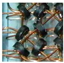
Figure: Close–Up of a Magnetic Core Memory [R40]
The IBM System/360 Model 85 and Cache
Memory
Although the development of magnetic core memory represented a significant
development in computer technology, it did not solve one of the essential
problems. There are two goals for the
development of a memory technology; it should be cheap and it should be fast. In general, these two goals are not
compatible.
The problem of providing a large inexpensive memory that appeared to be fast had been considered several times before it was directly addressed on the IBM System/360, Model 85. The System/360 family of third–generation computers will be discussed in some detail in the next pages; here we want to focus on its contribution to memory technology. Here we quote from the paper by J. S. Liptay [R58], published in 1968. In that paper, Liptay states:
“Among the objectives of the Model 85 is that of providing a System/360 compatible processor with both high performance and high throughput. One of the important ingredients of high throughput is a large main storage capacity. However, it is not feasible to provide a large main storage with an access time commensurate with the 80–nanosecond processor cycle of the Model 85. … [W]e decided to use a storage hierarchy. The storage hierarchy consists of a 1.04–microsecond main storage and a small, fast store called a cache, which is integrated into the CPU. The cache is not addressable by a program, but rather is used to hold those portions of main storage that are currently being used.”
The main storage unit for the computer was either an IBM 3265–5 or an IBM 2385, each of which had a capacity between 512 kilobytes and 4 megabytes. The cache was a 16 kilobyte integrated storage, capable of operating at the CPU cycle time of 80 nanoseconds. Optional upgrades made available a cache with either 24 kilobytes or 32 kilobytes.
Both the cache and main memory were divided into sectors, each holding 1 kilobyte of address space that was aligned on 1 KB address boundaries. Each sector was further divided into sixteen blocks of 64 bytes each; these correspond to what we now call “pages”. The cache memory was connected to the main memory via a 16–byte (128 bit) data path so that the processor could fetch or store an entire block in four requests to the main memory. The larger main memory systems were four–way interleaved, so that a request for a block was broken into four requests for 16 bytes each, and sent to each of the four memory banks.
While it required two processor cycles to fetch data in the cache (one to check for presence and one to fetch the data), it was normally the case that requests could be overlapped. In that case, the CPU could access data on every cycle.
In order to evaluate various cache management algorithms, the IBM engineers compared real computers to a hypothetical computer having a single large memory operating at cache speed. This was seen as the upper limit for the real Model 85. For a selected set of test programs, the real machine was seen to operate at an average of 81% of the theoretical peak performance; presumably meaning that it acted as if it had a single large memory with access time equal to 125% that of the cache access time.
Almost all future computers would be designed with a fast cache memory fronting a larger and slow memory. Later developments would show the advantage of having a split cache with an I–cache for instructions and a D–cache for data, as well as multilevel caches. We shall cover these advances in later chapters of the textbook; this is where it began
Interlude: Data Storage Technologies In the 1950’s
We have yet to address methods commonly used by early computers for storage of off–line data; that is data that were not actually in the main memory of the computer. One of the main methods was the use of 80 column punch cards, such as seen in the figure below.
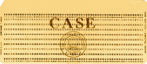
Figure: 80–Column Punch Card (Approximately
75% Size)
These cards would store at most eighty characters, so that the maximum data capacity was exactly eighty bytes. A decent sized program would require a few thousand of these cards to store the source code; these were transported in long boxes. On more than one occasion, this author has witnessed a computer operator drop a box of program cards, scattering the cards in random order and thus literally destroying the computer program.
Seven–Track Tapes and Nine–Track Tapes
Punched
cards were widely used by businesses to store account data up to the mid
1950’s. At some point, the requirement
to keep all of those punch cards became quite burdensome. One life insurance company reported that it
had to devote two floors of its modern skyscraper in
Data centers began to use larger magnetic tape drives for data storage. Early tape drives were called seven–track units in that they stored seven tracks of information on the tape: six tracks of data and one track of parity bits. Later designs stored eight data bits and parity.
The picture at left shows the first magnetic tape drive produced by IBM. This was the IBM 729, first released in 1952. The novelty of the design is reflected by an actual incident at the IBM receiving dock. The designers were expecting a shipment of magnetic tape when they were called by the foreman of the dock with the news that “We just received a shipment of tape from 3M, but are going to send it back … It does not have any glue on it”
The next picture shows a typical data center based on the IBM 7090 computer, in use from 1958 through 1969. Note the large number of tape drives. I can count at least 16.
The picky reader will note that the IBM 7090 is a Generation 2 computer that should not be discussed until the next section. We use the picture because the tape drives are IBM 729’s, first introduced in 1952, and because the configuration is typical of data centers of the time.
The IBM RAMAC
The next step in evolution of data storage is what became the disk drive. Again, IBM lead the way in developing this storage technology, releasing the RAMAC (Random Access Method for Accounting and Control) in 1956.
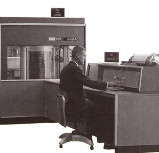
Figure: The RAMAC (behind the man’s head)
The RAMAC had fifty aluminum disks, each of which was 24 inches in diameter. Its storage capacity is variously quoted at 4.4MB or five million characters. At 5,000,000 characters we have 100,000 characters per 24–inch disk. Not very impressive for data density, but IBM had to start somewhere.
Vacuum Tube Computers (Generation
1 – a parting shot)
By the end of the first generation of computing machines in the middle 1950’s, most of the elements of a modern stored program computer had been put in place – the idea of a stored program, a reasonably efficient and reliable memory element, and the basic design of both the central processing unit and the I/O systems.
We leave this generation with a few personal memories of this author. First, there is the IBM 650, a vacuum-tube based computer in production from 1953 through 1962, when the last model was produced. This author recalls joining a research group in 1971, on the day an IBM 650 was being removed to storage to be replaced by a modern PDP–9.
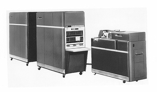
Figure: The IBM 650 – Power Supply, Main
Unit, and Read-Punch Unit
Source:
The reader will note that the I/O unit for the computer is labeled a “Read–Punch Unit”. The medium for communicating with this device was the punched card. Thus, the complete system had two components not seen here – a device for punching cards and a device for printing the contents of those cards onto paper for reading by humans.
It was also during the 1950’s that this author’s Ph.D. advisor, Joseph Hamilton, was a graduate student in a nuclear physics lab that had just received a very new multi-channel analyzer (a variant of a computer). He was told to move it and, unaware that it was top-heavy, managed to tip it over and shatter every vacuum tube in the device. This amounted to a loss of a few thousand dollars – not a good way to begin a graduate career.
One could continue with many stories, including the one about the magnetic drum unit on the first computer put on a sea-going U.S. Navy ship. The drum was spun up and everything was going well until the ship made an abrupt turn and the drum, being basically a large gyroscope, was ripped out of its mount and fell on the floor.
Discrete Transistor Computers
(Generation 2 – from 1958 to 1966)
The next generation of computers is based on a device called the transistor. Early forms of transistors had been around for quite some time, but were not regularly used due to a lack of understanding of the atomic structure of crystalline germanium. This author can recall use of an early germanium rectifier in a radio he built as a Cub Scout project – the instructions were to find the “sweet spot” on the germanium crystal for the “cat’s hair” rectifier. Early designs (before the late 1940’s) involved finding this “sweet spot” without any understanding of what made such a spot special. At some time in the 1940’s it was realized that there were two crystalline forms of germanium – called “P type” and “N type”. Methods were soon devised to produce crystals mostly of exactly one of the forms and transistors were possible.
The transistor was invented
by Walter Brattain and John Bardeen at Bell Labs in December 1947 and almost
instantly improved by William Shockley (also of Bell Labs) in February 1948. The transistor was announced to the world in
a press conference during June 1949. In
January 1951,
The next year, in April 1952, Bell Labs held the Transistor Technology Symposium. For eight days the attendees worked day and night to learn the tricks of building transistors. At the end of the symposium, they were sent home with a two volume book called “Transistor Technology” that later became known as “Mother Bell’s Cookbook”.
The previous two paragraphs were adapted from material on the Public Broadcast web page http://www.pbs.org/transistor/, which contains much additional material on the subject.
While transistors had
appeared in early test computers, such as the TX–0 built at MIT, it appears
that the first significant computer to use transistor technology was the IBM
7030, informally known at the “Stretch”.
Development of the Stretch was begun in 1955 with the goal of producing
a computer one hundred times faster than either the IBM 704 or IBM 705, the two
vacuum tube computers being sold by IBM at the time, for scientific and
commercial use respectively. While
missing its goal of being one hundred times faster, the IBM 7030 did achieve
significant speed gains by use of new technology. [R11]
1. By
switching to germanium transistor technology, the circuitry ran ten times
faster.
2. Memory
access became about six times faster, due to the use of core memory.
At this time, we pick up our
discussion of computer development by noting a series of computers developed
and manufactured by the Digital Equipment Corporation of
The technology used in these computers was a module comprised of a small number of discrete transistors and dedicated to one function. The following figure shows a module, called a Flip Chip by DEC, used on the PDP–8 in the late 1960’s.
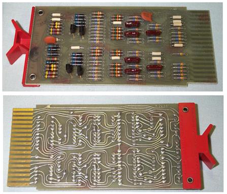
Figure: Front and Back of an R205b
Flip-Chip (Dual Flip-Flop) [R42]
In the above figure, one can easily spot many of the discrete components. The orange pancake-like items are capacitors, the cylindrical devices with colorful stripes are resistors with the color coding indicating their rating and tolerances, the black “hats” in the column second from the left are transistors, and the other items must be something useful. The size of this module is indicated by the orange plastic handle, which is fitted to a human hand.
These circuit cards were arranged in racks, as is shown in the next figure.
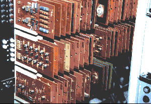
Figure: A Rack
of Circuit Cards from the Z–23 Computer (1961)
The PDP–8
was one of the world’s first minicomputers, so named because it was small
enough to fit on a desk. The name
“minicomputer” was suggested by the miniskirt, a
knee–length skirt much vogue during that time.
This author can say a lot of interesting things about miniskirts of that
era, but prefers to avoid controversy.
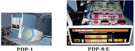
To show the size of a smaller minicomputer, we use a variant of the PDP–1 from about 1961 and the PDP–8/E (a more compact variant) from 1970. One can see that the PDP–1 with its line of cabinets is a medium–sized computer, while the PDP–8/E is rather small. It is worth note that one of the first video games, Spacewar by Steve Russell, was run on a PDP–1.
The
history of the development of DEC computers is well documented in a book titled
Computer Engineering: A DEC View of Hardware System Design, by C. Gordon Bell,
J. Craig Mudge, and John E. McNamara [R1].
DEC built a number of “families” of computers, including one line that
progressed from the PDP-5 to the PDP-8 and thence to the PDP-12. We shall return to that story after considering
the first and second generation computers that lead to the IBM System 360, one
of the first third generation computers.
The Evolution of the IBM–360
We now return to a discussion of “Big Iron”, a name given informally to the
larger IBM mainframe computers of the time.
Much of this discussion is taken from an article in the IBM Journal of
Research and Development [R46], supplemented by articles from [R1]. We trace the evolution of IBM computers from
the first scientific computer ( the IBM 701, announced in May 1952) through the
early stages of the S/360 (announced in March 1964).
We begin this discussion by considering the situation as of January 1, 1954. At the time, IBM has three models announced and shipping. Two of these were the IBM 701 for scientific computations and the IBM 702 for financial calculations (announced in September 1953),. Each of the designs used Williams–Kilburn tubes for primary memory, and each was implemented using vacuum tubes in the CPU. Neither computer supported both floating–point (scientific) and packed decimal (financial) arithmetic, as the cost to support both would have been excessive. As a result, there were two “lines”: scientific and commercial.
The third model was the IBM 650, mentioned and pictured in the above discussion of the first generation. It was designed as “a much smaller computer that would be suitable for volume production. From the outset, the emphasis was on reliability and moderate cost”. The IBM 650 was a serial, decimal, stored–program computer with fixed length words each holding ten decimal digits and a sign. Later models could be equipped with the IBM 305 RAMAC (the disk memory discussed and pictured above). When equipped with terminals, the IBM 650 started the shift towards transaction–oriented processing.
The
figure below can be considered as giving the “family tree” of the IBM
System/360.
Note that there are four “lines”: the IBM 650 line, the IBM 701 line, IBM 702
line, and the IBM 7030 (Stretch). The System/360 (so named because it handled
“all 360 degrees of computing”) was an attempt to consolidate these lines and
reduce the multiplicity of distinct systems, each with its distinct maintenance
problems and costs.
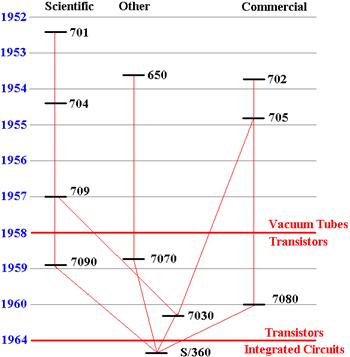
Figure: The IBM
System/360 “Family Tree”
As mentioned above, in the 1950’s IBM supported two product lines: scientific computers (beginning with the IBM 701) and commercial computes (beginning with the IBM 702). Each of these lines was redesigned and considerably improved in 1954.
Generation 1 of the Scientific Line
In the IBM 704 (announced in May 1954), the Williams–Kilburn tube memory was
replaced by magnetic–core memory with up to 32768 36–bit words. This eliminated the most difficult
maintenance problem and allowed users to run larger programs. At the time, theorists had estimated that a
large computer would require only a few thousand words of memory. Even at this time, the practical programmers
wanted more than could be provided.
The IBM 704 also introduced hardware support for floating–point arithmetic, which was omitted from the IBM 701 in an attempt to keep the design “simple and spartan” [R46]. It also added three index registers, which could be used for loops and address modification. As many scientific programs make heavy use of loops over arrays, this was a welcome addition.
The IBM 709 (announced in January 1957) was basically an upgraded IBM 704. The most important new function was then called a “data–synchronizer unit”; it is now called an “I/O Channel”. Each channel was an individual I/O processor that could address and access main memory to store and retrieve data independently of the CPU. The CPU would interact with the I/O Channels by use of special instructions that later were called channel commands.
It was this flexibility, as much as any other factor, that lead to the development of a simple supervisory program called the IOCS (I/O Control System). This attempt to provide support for the task of managing I/O channels and synchronizing their operation with the CPU represents an early step in the evolution of the operating system.
Generation 1 of the Commercial Line
The IBM 702 series differed from the IBM 701 series in many ways, the most
important of which was the provision for variable–length digital
arithmetic. In contrast to the 36–bit
word orientation of the IBM 701 series, this series was oriented towards
alphanumeric arithmetic, with each character being encoded as 6 bits with an
appended parity check bit. Numbers could
have any length from 1 to 511 digits, and were terminated by a “data mark”.
The IBM 705 (announced in October 1954) represented a considerable upgrade to the 702. The most significant change was the provision of magnetic–core memory, removing a considerable nuisance for the maintenance engineers. The size of the memory was at first doubled and then doubled again to 40,000 characters. Later models could be provided with one or more “data–synchronizer units”, allowing buffered I/O independent of the CPU.
Generation 2 of the Product Lines
As noted above, the big change associated with the transition to the second
generation is the use of transistors in the place of vacuum tubes. Compared to an equivalent vacuum tube, a
transistor offers a number of significant advantages: decreased power usage,
decreased cost, smaller size, and significantly increased reliability. These advantages facilitated the design of
increasingly complex circuits of the type required by the then new second
generation.
The IBM 7070 (announced in September 1958 as an upgrade to the IBM 650) was the first transistor based computer marketed by IBM. This introduced the use of interrupt–driven I/O as well as the SPOOL (Simultaneous Peripheral Operation On Line) process for managing shared Input/Output devices.
The IBM 7090 (announced in December 1958) was a transistorized version of the IBM 709 with some additional facilities. The IBM 7080 (announced in January 1960) likewise was a transistorized version of the IBM 705. Each model was less costly to maintain and more reliable than its tube–based predecessor, to the extent that it was judged to be a “qualitatively different kind of machine” [R46].
The IBM 7090 (and later IBM 7094) were modified by researchers at M.I.T. in order to make possible the CTSS (Compatible Time–Sharing System), the first major time–sharing system. Memory was augmented by a second 32768–word memory bank. User programs occupied one bank while the operating system resided in the other. User memory was divided into 128 memory–protected blocks of 256 words, and access was limited by boundary registers.
The IBM 7094 was announced on January 15, 1962. The CTSS effort was begun in 1961, with a version being demonstrated on an IBM 709 in November 1961. CTSS was formally presented in a paper at the Joint Computer Conference in May, 1962. Its design affected later operating systems, including MULTICS and its derivatives, UNIX and MS–DOS.
As a last comment here, the true IBM geek will note the omission of any discussion of the IBM 1401 line. These machines were often used in conjunction with the 7090 or 7094, handling the printing, punching, and card reading chores for the latter. It is just not possible to cover every significant machine.
The IBM 7030 (Stretch)
In late 1954, IBM decided to undertake a very ambitious research project,
with the goal of benefiting from the experience gained in the previous three
project lines. In 1955, it was decided
that the new machine should be at least 100 times as fast as either the IBM 704
or the IBM 705; hence the informal name “Stretch” as it “stretched the
technology”.
In order to achieve these goals, the design of the IBM 7030 required a considerable number of innovations in technology and computer organization; a few are listed here.
1. A
new type of germanium transistor, called “drift transistor” was developed. These
faster transistors allowed
the circuitry in the Stretch to run ten times faster.
2. A new type of core memory was developed; it was 6 times faster than the older core.
3. Memory
was organized into multiple 128K–byte units accessed by low–order
interleaving, so that
successive words were stored in different banks. As a result,
new data could be retrieved
at a rate of one word every 200 nanoseconds, even
though the memory cycle time
was 2.1 microseconds (2,100 nanoseconds).
4. Instruction
lookahead (now called “pipelining”) was introduced. At any point in
time, six instructions were
in some phase of execution in the CPU.
5. New
disk drives, with multiple read/write arms, were developed. The capacity and
transfer rate of these
devices lead to the abandonment of magnetic drums.
6. A
pair of boundary registers were added so as to provide the storage protection
required in a
multiprogramming environment.
It is generally admitted that the Stretch did not meet its design goal of a 100 times increase in the performance of the earlier IBM models. Here is the judgment by IBM from 1981 [R46].
“For a typical 704 program, Stretch fell short of is performance target of one hundred times the 704, perhaps by a factor of two. In applications requiring the larger storage capacity and word length of Stretch, the performance factor probably exceeded one hundred, but comparisons are difficult because such problems were not often tackled on the 704.” [R46]
It seems that production of the IBM 7030 (Stretch) was limited to nine machines, one for Los Alamos National Labs, one (called “Harvest”) for the National Security Agency, and 7 more.
Interlude:
The Evolution of the PDP–8
While this story does not exactly fit here, it serves as a valuable example
of the transition from the second generation of computers to later
generations. We quickly trace the CPU
size of the PDP–8 computer by the Digital Equipment Corporation from its
predecessor (the
PDP–5, introduced in 1963), through the first PDP–8 (1964), to a later
implementation.
According
to
In 1971, the PDP-8/E (a smaller version of the PDP-8) had only three boards with 240 square inches of circuit space for the CPU. In 1976, the Intersil Corporation produced a fully-functioning PDP-8 CPU on a single chip, about 1/4 inch on a side. Thus we have a more powerful CPU on a form factor that is reduced in scale by a factor of 33,600.
Smaller Integrated (SSI and MSI) Circuits (Generation 3 – from 1966
to 1972)
In one sense, the evolution of computer components can be said to have stopped in 1958 with the introduction of the transistor; all future developments merely represent the refinement of the transistor design. This statement stretches the truth so far that it hardly even makes this author’s point, which is that packaging technology is extremely important.
What we see in the generations following the introduction of the transistor is an aggressive miniaturization of both the transistors and the traces (wires) used to connect the circuit elements. This allowed the creation of circuit modules with component densities that could hardly have been imagined a decade earlier. Such circuit modules used less power and were much faster than those of the second generation; in electronics smaller is faster. They also lent themselves to automated manufacture, thus increasing component reliability.
It seems that pictures are the best way to illustrate the evolution of the first three generations of computer components. Below, we see a picture of an IBM engineer (they all wore coats and ties at that time) with three generations of components.
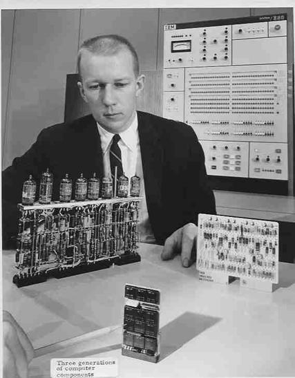
Figure: IBM
Engineer with Three Generations of Components
The first generation unit (vacuum tubes) is a pluggable module from the IBM 650. Recall that the idea of pluggable modules dates to the ENIAC; the design facilitates maintenance.
The second generation unit (discrete transistors) is a module from the IBM 7090.
The third generation unit is the ACPX module used on the IBM 360/91 (1964). Each chip was created by stacking layers of silicon on a ceramic substrate; it accommodated over twenty transistors. The chips could be packaged together onto a circuit board. The circuit board in the foreground appears to hold twelve chips. This author conjectures, but cannot prove that the term “ACPX module” refers to the individual chip, and that the pencil in the foreground is indicating one such module.
It is likely that each of the chips on the third–generation board has a processing power equivalent to either of the units from the previous generations.
The
74181 Arithmetic Logic Unit by
The first real step in the third generation of computing was taken when
Texas Instruments introduced the 7400 series of integrated circuits. One of the earliest, and most famous, was a
MSI chip called the 74181. It was an
arithmetic logic unit (ALU) that provided thirty–two functions of two 4–bit
variables, though many of those functions were quite strange. It was developed in the middle 1960’s and
first used in the Data General Nova computer in 1968.
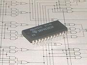
Figure: The
74181 in a DIP Packaging
The figure above shows the chip in its DIP (Dual In–line Pin) packaging. The figure below shows the typical dimensions of a chip in the DIP configuration.
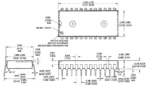
Figure: The 74181 Physical Dimensions in
Inches (Millimeters)
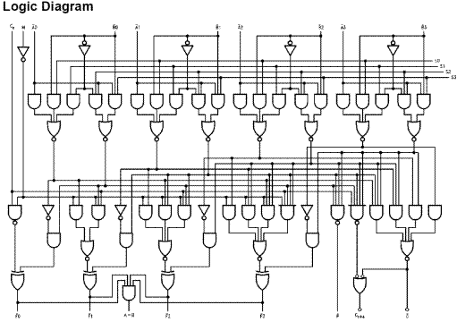
For those who like circuit diagrams, here is a circuit diagram of the 74181 chip. A bit later in the textbook, we shall discuss how to read this diagram; for now note that it is moderately complex, comprising seventy five logic gates.
Here is a long description of the 74181, taken from the Wikipedia article.
“The 74181
is a 7400 series medium-scale integration (MSI) TTL integrated circuit,
containing the equivalent of 75 logic gates and most commonly packaged as a
24-pin DIP. The 4-bit wide ALU can perform all the traditional add / subtract /
decrement operations with or without carry, as well as AND /
The 74181 performs these
operations on two four bit operands generating a four bit result with carry in
22 nanoseconds. The 74S181 performs the same operations in 11 nanoseconds.
Multiple 'slices' can be
combined for arbitrarily large word sizes. For example, sixteen 74S181s and
five 74S182 look ahead carry generators can be combined to perform the same
operations on 64-bit operands in 28 nanoseconds. Although overshadowed by the
performance of today's multi-gigahertz 64-bit microprocessors, this was quite
impressive when compared to the sub megahertz clock speeds of the early four
and eight bit microprocessors
Although the 74181 is only an ALU
and not a complete microprocessor it greatly simplified the development and
manufacture of computers and other devices that required high speed computation
during the late 1960s through the early 1980s, and is still referenced as a
"classic" ALU design.
Prior to the introduction of
the 74181, computer CPUs occupied multiple circuit boards and even very simple
computers could fill multiple cabinets. The 74181 allowed an entire CPU and in
some cases, an entire computer to be constructed on a single large printed
circuit board. The 74181 occupies a historically significant stage between
older CPUs based on discrete logic functions spread over multiple circuit
boards and modern microprocessors that incorporate all CPU functions in a
single component. The 74181 was used in various minicomputers and other devices
beginning in the late 1960s, but as microprocessors became more powerful the
practice of building a CPU from discrete components fell out of favor and
the 74181 was not used in any new designs.
Many computer CPUs and
subsystems were based on the 74181, including several historically significant
models.
1. NOVA
- First widely available 16-bit minicomputer manufactured by
Data General. This was the first
design (in 1968) to use the 74181.
2. PDP-11
- Most popular minicomputer of all time, manufactured by
Digital Equipment Corporation. The first model was introduced in 1970.
3. Xerox
Alto - The first computer to use the desktop metaphor and graphical
user interface (GUI).
4. VAX
11/780 - The first VAX, the most popular 32-bit computer of the
1980s[8], also manufactured by Digital Equipment
Corp.”
Back to the System/360
Although the System/360
likely did not use any 74181’s, that chip does illustrate the complexity of the
custom–fabricated chips used in IBM’s design.
The design goals for the System/360 family are illustrated by the following scenario. Imagine that you have a small company that is using an older IBM 1401 for its financial work. You want to expand and possibly do some scientific calculations. Obviously, IBM is very happy to lease you a computer. We take your company through its growth.
1. At first, your company needs only a small
computer to handle its computing
needs. You lease an IBM System 360/30. You use it in emulation
mode to run your IBM 1401
programs unmodified.
2. Your company grows. You need a bigger computer. Lease a 360/50.
3. You hit the “big time”. Turn in the 360/50 and lease a 360/91.
You never need to rewrite
or recompile your existing programs.
You can still run your IBM
1401 programs without modification.
In order to understand how the System/360 was able to address these concerns, we must divert a bit and give a brief description of the control unit of a stored program computer.
The
Control Unit and Emulation
In order to better explain one of the distinctive features of the IBM
System/360 family, it is necessary to take a detour and discuss the function of
the control unit in a stored program computer.
Basically, the control unit tells the computer what to do.
All modern stored program computers execute programs that are a sequence of binary machine–language instructions. This sequence of instructions corresponds either to an assembly language program or a program in a higher–level language, such as C++ or Java.
The basic operation of a stored program computer is called “fetch–execute”, with many variants on this name. Each instruction to be executed is fetched from memory and deposited in the Instruction Register, which is a part of the control unit. The control unit interprets this machine instruction and issues the signals that cause the computer to execute it.
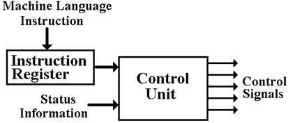
Figure:
Schematic of the Control Unit
There are two ways in which a control unit may be organized. The most efficient way is to build the unit entirely from basic logic gates. For a moderately–sized instruction set with the standard features expected, this leads to a very complex circuit that is difficult to test.
In 1951, Maurice V. Wilkes (designer of the EDSAC, see above) suggested an organization for the control unit that was simpler, more flexible, and much easier to test and validate. This was called a “microprogrammed control unit”. The basic idea was that control signals can be generated by reading words from a micromemory and placing each in an output buffer.
In this design, the control unit interprets the machine language instruction and branches to a section of the micromemory that contains the microcode needed to emit the proper control signals. The entire contents of the micromemory, representing the sequence of control signals for all of the machine language instructions is called the microprogram. All we need to know is that the microprogram is stored in a ROM (Read Only Memory) unit.
While microprogramming was sporadically investigated in the 1950’s, it was not until about 1960 that memory technology had matured sufficiently to allow commercial fabrication of a micromemory with sufficient speed and reliability to be competitive. When IBM selected the technology for the control units of some of the System/360 line, its primary goal was the creation of a unit that was easily tested. Then they got a bonus; they realized that adding the appropriate blocks of microcode could make a S/360 computer execute machine code for either the IBM 1401 or IBM 7094 with no modification. This greatly facilitated upgrading from those machines and significantly contributed to the popularity of the S/360 family.
The IBM System/360
As noted above, the IBM chose to replace a number of very successful, but
incompatible, computer lines with a single computer family, the
System/360. The goal, according to an
IBM history web site [R48] was to “provide an expandable system that would
serve every data processing need”. The
initial announcement on April 7, 1964 included Models 30, 40, 50, 60, 62, and 70
[R49]. The first three began shipping in
mid–1965, and the last three were replaced by the Model 65 (shipped in November
1965) and Model 75 (January 1966).
The introduction of the
System/360 is also the introduction of the term “architecture”
as applied to computers. The following
quotes are taken from one of the first papers
describing the System/360 architecture [R46].
“The
term architecture
is used here to describe the attributes of a system as seen by
the programmer,, i.e., the conceptual structure and functional behavior, as
distinct
from the organization of the data flow and controls, the logical design,
and the physical implementation.”
“In the
last few years, many computer architects have realized, usually implicitly,
that logical structure (as seen by the programmer) and physical structure (as
seen
by the engineer) are quite different.
Thus, each may see registers, counters, etc.,
that to the other are not at all real entities.
This was not so in the computers of the
1950’s. The explicit recognition of the
duality of the structure opened the way
for the compatibility within System/360.”
At this point, we differentiate between the three terms: architecture, organization, and implementation. The quote above gives a precise comparison of the terms architecture and organization. As an example, consider the sixteen general–purpose registers (R0 – R15) in the System/360 architecture. All models implement these registers and use them in exactly the same way; this is a requirement of the architecture. As a matter of implementation, a few of the lower end S/360 family actually used dedicated core memory for the registers, while the higher end models used solid state circuitry on the CPU board.
The difference between organization and implementation is seen by considering the two computer pairs: the 709 and 7090, and the 705 and 7080. The IBM 7090 had the same organization (hence the same architecture) as the IBM 709; the implementation was different. The IBM 709 used vacuum tubes; the IBM 7090 replaced these with transistors.
The requirement for the
System/360 design is that all models in that series would be
“strictly program compatible, upward and downward, at the program bit
level”. [R46]
“Here it
[strictly program compatible] means that a valid program, whose logic will
not depend implicitly upon time of execution and which runs upon configuration
A,
will also run on configuration B if the latter includes as least the required
storage, at
least the required I/O devices, and at least the required optional features.”
“Compatibility
would ensure that the user’s expanding needs be easily accommodated
by any model. Compatibility would also
ensure maximum utility of programming
support prepared by the manufacturer, maximum sharing of programs generated by
the user, ability to use small systems to back up large ones, and exceptional
freedom in configuring systems for particular applications.”
Additional design goals for the System/360 include the following.
1. The System/360 was intended to replace two mutually incompatible
product
lines in existence at the
time.
a) The scientific series (701, 704, 7090, and
7094) that supported floating
point arithmetic,
but not decimal arithmetic.
b) The commercial series (702, 705, and 7080)
that supported decimal
arithmetic, but
not floating point arithmetic.
2. The System/360 should have a
“compatibility mode” that would allow it
to run unmodified machine
code from the IBM 1401 – at the time a very
popular business machine
with a large installed base.
This
was possible due to the use of a microprogrammed control unit. If you
want to run native S/360
code, access that part of the microprogram.
If you
want to run IBM 1401 code,
just switch to the microprogram for that machine.
3. The Input/Output Control Program should be
designed to allow execution by
the CPU itself (on smaller
machines) or execution by separate I/O Channels
on the larger machines.
4. The system must allow for autonomous
operation with very little intervention by
a human operator. Ideally this would be limited to mounting and
dismounting
magnetic tapes, feeding
punch cards into the reader, and delivering output.
5. The system must support some sort of
extended precision floating point
arithmetic, with more
precision than the 36–bit system then in use.
Minicomputers: the Rise and
Fall of the VAX
So far, our discussion of the third generation of computing has focused on
the mainframe, specifically the IBM System/360.
Later, we shall mention another significant large computer of this
generation; the CDC–6600. For now, we
turn our attention to the minicomputer, which represents another significant
development of the third generation.
Simply, these computers were smaller and lest costly than the “big
iron”.
In 1977, Gordon Bell provided a definition of a minicomputer [R1, page 14].
“[A minicomputer is a] computer originating in the early 1960s and predicated on being the lowest (minimum) priced computer built with current technology. From this origin, at prices ranging from 50 to 100 thousand dollars, the computer has evolved both at a price reduction rate of 20 percent per year …”
The above definition seems to ignore microcomputers; probably these were not “big players” at the time it was made. From the modern perspective, the defining characteristics of a minicomputer were relatively small size and modest cost.
As noted above, the PDP–8 by Digital Equipment Corporation is considered to be the first minicomputer. The PDP–11 followed in that tradition.
This discussion focuses on the VAX series of computers, developed and marketed by the Digital Equipment Corporation (now out of business), and its predecessor the PDP–11. We begin with a discussion of the PDP–11 family, which was considered to be the most popular minicomputer; its original design was quite simple and elegant. We then move to a discussion of the Virtual Address Extension (VAX) of the PDP–11, note its successes, and trace the reasons for its demise. As we shall see, the major cause was just one bad design decision, one that seemed to be very reasonable when it was first made.
The Programmable Data Processor 11, introduced in 1970, was
an outgrowth of earlier lines of small computers developed by the Digital
Equipment Corporation, most notably the
PDP–8 and PDP–9. The engineers made a
survey of these earlier designs and made a conscious decision to fix what were
viewed as design weaknesses. As with IBM
and its System/360, DEC decided on a family of compatible computers with a wide
range of price ($500 to $250,000) and performance. All members of the PDP–11 family were
fabricated from TTL integrated circuits; thus the line was definitely
third–generation.
The first model in the line was the PDP–11/20, followed soon by the PDP–11/45, a model designed for high performance. By 1978, there were twelve distinct models in the PDP–11 line (LSI–11, PDP–11/04, PDP–11/05, PDP–11/20, PDP–11/34, PDP–11/34C, PDP–11/40, PDP–11/45, PDP–11/55, PDP–11/60, PDP–11/70, and the VAX–11/780). Over 50,000 of the line had been sold, which one of the developers (C. Gordon Bell), considered a qualified success, “since a large and aggressive marketing organization, armed with software to correct architectural inconsistencies and omissions, can save almost any design”[R1, page 379].
With the exception of the
VAX–11/780 all members of this family were essentially 16–bit machines with
16–bit address spaces. In fact, the
first of the line (the PDP–11/20) could address only 216 = 65536
bytes of memory. Given that the top 4K
of the address space was mapped for I/O devices, the maximum amount of physical
memory on this machine was
61,440 bytes. Typically, with the
Operating System installed, this left about 32 KB space for user programs. While many programs could run in this space,
quite a few could not.
According to two of the PDP–11’s developers:
“The first weakness of minicomputers was their limited addressing capability. The PDP–11 followed this hallowed tradition of skimping on address bits, but it was saved by the principle that a good design can evolve through at least one major change. … It is extremely embarrassing that the PDP–11 had to be redesigned with memory management [used to convert 16–bit addresses into 18–bit and then 22–bit addresses] only two years after writing the paper that outlined the goal of providing increased address space.”[R1, page 381]
While the original PDP–11 design
was patched to provide first an 18–bit address space (the
PDP–11/45 in 1972) and a 22–bit address space (the PDP–11/70 in 1975), it was
quickly obvious that a new design was required to solve the addressability
problem. In 1974, DEC started work on
extending the virtual address space of the PDP–11, with the goal of a computer
that was compatible with the existing PDP–11 line. In April 1975, work was redirected to produce
a machine that would be “culturally compatible with the PDP–11”. The result was the VAX series, the first
model of which was the VAX–11/780, which was introduced on October 25, 1977. At the time, it was called a “super–mini”;
its later models, such as the VAX–11/9000 series were considered to be
mainframes.
By 1982 Digital Equipment Corporation was the number two computer company. IBM maintained it's lead as number one. The VAX series of computers, along with its proprietary operating system, VMS, were the company sales leaders. One often heard of “VAX/VMS”.
The VAX went through many
different implementations. The original VAX was implemented in TTL and filled
more than one rack for a single CPU. CPU implementations that consisted of
multiple ECL gate array or macrocell array chips included the 8600, 8800 super–minis
and finally the 9000 mainframe class machines. CPU implementations that
consisted of multiple MOSFET custom chips included the 8100 and 8200 class
machines. The computers in the VAX line
were excellent machines, supported by well–designed and stable operating
systems. What happened? Why did they disappear?
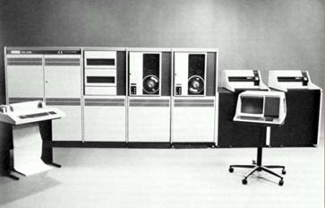
Figure: A
Complete VAX–11/780 System
In order to understand the reason for the demise of the VAX line of computers, we must first present some of its design criteria, other than the expanded virtual address space. Here we quote from Computer Architecture: A Quantitative Approach by Hennessy & Patterson.
“In the late 1960’s and early 1970’s, people realized that software costs
were growing faster than hardware costs.
In 1967, McKeeman argued that compilers and operating systems were
getting too big and too complex and taking too long to develop. Because of inferior compilers and the memory
limitations of computers, most system programs at the time were still written
in assembly language. Many researchers
proposed alleviating the software crisis by creating more powerful, software–oriented
architectures.
In 1978, Strecker
discussed how he and the other architects at DEC responded to this by designing
the VAX architecture. The VAX was
designed to simplify compilation of high–level languages. … The VAX architecture was designed to be
highly orthogonal and to allow the mapping of high–level–language statements
into single VAX instructions.” [R60, page 126]
What we see here is the demand for what
would later be called a CISC design. In
a Complex Instruction Set Computer, the ISA (Instruction Set
Architecture) provides features to support a high–level language, and minimize
what was called the “semantic gap”.
The VAX has been perceived as the
quintessential CISC processing architecture, with its very large number of addressing
modes and machine instructions, including instructions for such complex
operations as queue insertion/deletion and polynomial evaluation. Eventually, it was this complexity that
caused its demise. As we shall see
below, this complexity was not required or even found useful.
The eventual downfall of the VAX line was
due to the CPU design philosophy called “RISC”, for Reduced Instruction Set
Computer. As we shall see later in the
text, there were many reasons for the RISC movement, among them the fact that
the semantic gap was more a fiction of the designers imagination than a
reality. What compiler writers wanted
was a clean CPU design with a large number of registers and possibly a good
amount of cache memory. None of these
features were consistent with a CISC design, such as the VAX.
The bottom line was that the new RISC
designs offered more performance for less cost than the VAX line of
computers. Most of the new designs,
including those based on the newer Intel CPU chips, were also smaller and easier
to manage. The minicomputers that were
so popular in the 1970’s and 1980’s had lost their charm to newer and smaller
models.
DEC came late to the RISC design arena,
marketing the Alpha in 1992, a 64 bit machine.
By then it was too late. Most
data centers had switched to computers based on the Intel chips, such as the
80486/80487 or the Pentium. The epitaph
for DEC is taken from Wikipedia.
“Although many of these products were well designed, most of them were DEC–only
or DEC–centric, and customers frequently ignored them and used third-party
products instead. Hundreds of millions of dollars were spent on these projects,
at the same time that workstations based on RISC architecture were starting to
approach the VAX in performance. Constrained by the huge success of their
VAX/VMS products, which followed the proprietary model, the company was very
late to respond to commodity hardware in the form of Intel-based personal
computers and standards-based software such as Unix as well as Internet
protocols such as TCP/IP. In the early 1990s, DEC found its sales faltering and
its first layoffs followed. The company that created the minicomputer, a
dominant networking technology, and arguably the first computers for personal
use, did not effectively respond to the significant restructuring of the computer
industry.”
“Beginning in 1992, many of DEC’s assets were spun off in order to raise
revenue. This did not stem the tide of
red ink or the continued lay offs of personnel.
Eventually, on January 26, 1998, what remained of the company was sold to Compaq Computer Corporation. In August 2000, Compaq announced that the
remaining VAX models would be discontinued by the end of the year. By 2005 all manufacturing of VAX computers had
ceased, but old systems remain in widespread use. Compaq was sold to Hewlett–Packard in 2002.”
It was the end of an era; minicomputers had left the scene.
Large Scale and Very
Large Scale Integrated Circuits (from 1972 onward)
We now move to a discussion of LSI and VLSI circuitry. We could trace the development of the third generation System/360 through later, more sophisticated, implementations. Rather than doing this, we shall trace the development of another iconic processor series, the Intel 4004, 8008, and those that followed.
The most interesting way to describe the beginning of the fourth generation of technology, that of a microprocessor on a chip [R1], is to quote from preface to the 1995 history of the microcomputer written by Stanley Mazor [R61], who worked for Intel from 1969 to 1984.
“Intel’s founder, Robert Noyce, chartered Ted Hoff’s Applications Research Department in 1969 to find new applications for silicon technology – the microcomputer was the result. Hoff thought it would be neat to use MOS LSI technology to produce a computer. Because of the ever growing density of large scale integrated (LSI) circuits, a ‘computer on a chip’ was inevitable. But in 1970 we could only get about 2000 transistors on a chip and a conventional CPU would need about 10 times that number. We developed two ‘microcomputers’ 10 years ahead of ‘schedule’ by scaling down the requirements and using a few other ‘tricks’ described in this paper.”
Intel delivered two Micro Computer Systems in the early 1970’s. The first was the MCS–4, emphasizing low cost, in November 1971. This would lead to a line of relatively powerful but inexpensive controllers, such as the Intel 8051 (which in quantity sells for less than $1). The other was the MCS–8, emphasizing versatility, in April 1972. This lead to the Intel 8008, 8080, 8086, 80286, and a long line of processors for personal computers.
The MCS–4
was originally developed in response to a demand for a chip to operate a
hand–held calculator. It was a four–bit
computer, with four–bit data memory, in response to the use of 4–bit BCD codes
to represent the digits in the calculator.
The components of the
MCS–4 included the 4001 (Read Only Memory), 4002 (Random Access Memory), and
the 4004 Microprocessor. Each was
mounted in a 16–pin package, as that was the only package format available in the
company at the time.
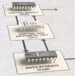
Figure: Picture
from the 1972 Spec Sheet on the MCS–4
In 1972, the Intel 4004 sold in quantity for less than $100 each. It could add two 10–digit numbers in about 800 microseconds. This was comparable to the speed of the IBM 1620, a computer that sold for $100,000 in 1960.
The MCS–8 was based on the Intel 8008, Intel’s first 8–bit CPU. It was implemented with TTL technology, had 48 instructions, and had a performance rating of 0.06 MIPS (Million Instructions per Seconds, a term not in use at the time). It had an 8–bit accumulator and six 8–bit general purpose registers (B, C, D, E, H, and L). In later incarnations of the model, these would become the 8–bit lower halves of the 16–bit registers with the same name.
The Intel 8008 was placed in an 18–pin package. It is noteworthy that the small pin counts available for the packaging drove a number of design decisions, such as multiplexing the bus. In this, the bus connecting the CPU to the memory chip has at least two uses, and a control signal to indicate what signals are on the bus.
The 8008 was followed by the 8080, which had ten times the performance and was housed in a 40–pin plastic package, allowing separate lines for bus address and bus data. The 8080 did not yet directly support 16–bit processing, but arranged its 8–bit registers in pairs. The 8080 was followed by the 8085 and then by the 8086, a true 16–bit CPU. The 8088 (an 8086 variant with a 8–bit data bus) was selected by IBM for its word processor; the rest is history.
As we know, the 8086 was the first in a sequence of processors with increasing performance. The milestones in this line were the 80286, the 80386 (the first with true 32–bit addressing), the 80486/80487, and the Pentium. The line will soon implement 64–bit addressing.
The major factor driving the development of smaller and more powerful computers was and continues to be the method for manufacture of the chips. This is called “photolithography”, which uses light to transmit a pattern from a photomask to a light–sensitive chemical called “photoresist” that is covering the surface of the chip. This process, along with chemical treatment of the chip surface, results in the deposition of the desired circuits on the chip.
Due to a fundamental principle of Physics, the minimum feature size that can be created on the chip is approximately the same as the wavelength of the light used in the lithography. State–of–the–art (circa 2007) photolithography uses deep ultraviolet light with wavelengths of 248 and 193 nanometers, resulting in feature sizes as small as 50 nanometers [R53]. An examination of the table on the next page shows that the minimum feature size seems to drop in discrete steps in the years after 1971; each step represents a new lithography process.
One
artifact of this new photolithography process is the enormous cost of the plant
used to fabricate the chips. In the
terminology of semiconductor engineering, such a plant is called a “fab”. In 1998, Gordon Moore of Intel Corporation
(and
“An R&D fab today costs $400 million just for the building. Then you put about $1 billion of equipment in it. That gives you a quarter–micron [250 nanometer] fab for about 5,000 wafers per week, about the smallest practical fab.”
The “quarter–micron fab” represents the ability to create chips in which the smallest line feature has a size of 0.25 micron, or 250 nanometers.
One can describe the VLSI generation of computers in many ways, all of them interesting. However, the most telling description is to give the statistics of a line of computers and let the numbers speak for themselves. The next two pages do just that for the Intel line.
Here are the raw statistics, taken from a Wikipedia article [R52].
|
Model |
Introduced |
MHz |
Transistors |
Line Size |
|
4004 |
11/15/1971 |
0.74 |
2,300 |
10.00 |
|
8008 |
4/1/1972 |
0.80 |
3,500 |
10.00 |
|
8080 |
4/1/1974 |
2.00 |
6,000 |
6.00 |
|
8086 |
6/8/1976 |
10.00 |
29,000 |
3.00 |
|
80286 |
2/1/1982 |
25.00 |
134,000 |
1.50 |
|
80386 |
10/17/1985 |
16.00 |
275,000 |
1.00 |
|
80386 |
4/10/1989 |
33.00 |
275,000 |
1.00 |
|
80486 |
6/24/1991 |
50.00 |
1,200,000 |
0.80 |
|
Pentium |
3/23/1993 |
66.00 |
3,200,000 |
0.60 |
|
Pentium Pro |
11/1/1995 |
200.00 |
5,500,000 |
0.35 |
|
Pentium II |
5/7/1997 |
300.00 |
7,500,000 |
0.35 |
|
Pentium II |
8/24/1998 |
450.00 |
7,500,000 |
0.25 |
|
Pentium III |
2/26/1999 |
450.00 |
9,500,000 |
0.25 |
|
Pentium III |
10/25/1999 |
733.00 |
28,100,000 |
0.18 |
|
Pentium 4 |
11/20/2000 |
1500.00 |
42,000,000 |
0.18 |
|
Pentium 4 |
1/7/2002 |
2200.00 |
55,000,000 |
0.13 |
|
Pentium 4F |
2/20/2005 |
3800.00 |
169,000,000 |
0.09 |
Here is the obligatory
chart, illustrating
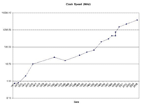
Two other charts are equally
interesting. The first shows the
increase in clock speed as a function of time.
Note that this chart closely resembles the
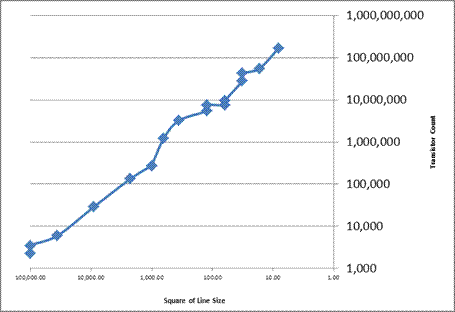
 The second chart shows an entirely expected relationship
between the line size on the die and the number of transistors placed on
it. The count appears to be a direct
function of the size.
The second chart shows an entirely expected relationship
between the line size on the die and the number of transistors placed on
it. The count appears to be a direct
function of the size.
Dual Core and Multi–Core CPU’s
Almost all of the VLSI central processors on a chip that we have discussed to this point could be called “single core” processors; the chip had a single CPU along with some associated cache memory. Recently there has been a movement to multi–core CPU’s, which represent the placement of more than one CPU on a single chip. One might wonder why this arrangement seems to be preferable to a single faster CPU on the chip.
In order to understand this phenomenon, we quote from a 2005 advertisement by Advanced Micro Devices (AMD), Inc. for the AMD 64 Opteron chip, used in many blade servers. This article describes chips by the linear size of the thinnest wire trace on the chip; a 90nm chip has features with a width of 90 nanometers, or 0.090 microns. Note also that it mentions the issue of CPU power consumption; heat dissipation has become a major design issue.
“Until recently, chip suppliers emphasized the frequency of their chips (“megahertz”) when discussing speed. Suddenly they’re saying megahertz doesn’t matter and multiple cores are the path to higher performance. What changed? Three factors have combined to make dual-core approaches more attractive.”
“First, the shift to 90nm process technology makes dual-core possible. Using 130nm technology, single-core processors measured about 200 mm2, a reasonable size for a chip to be manufactured in high-volumes. A dual-core 130nm chip would have been about 400 mm2, much too large to be manufactured economically. 90nm technology shrinks the size of a dual-core chip to under 200 mm2 and brings it into the realm of possibility.”
“Second, the shift to dual-core provides a huge increase in CPU performance. Increasing frequency by 10 percent (often called a “speed bump”) results in at best a 10 percent boost in performance; two speed bumps can yield a 20 percent boost. Adding a second core can boost performance by a factor of 100 percent for some workloads.”
“Third, dual-core processors can deliver far more performance per watt of power consumed than single core designs, and power has become a big constraint on system design. All other things being equal, CPU power consumption increases in direct relation to clock frequency; boosting frequency by 20 percent boosts power by a least 20 percent. In practice, the power consumption situation is even worse. Chip designers need extra power to speed up transistor performance in order to attain increased clock frequencies; a 20 percent boost in frequency might require a 40 percent boost in power.”
“Dual-core designs apply this principle in reverse; they lower the frequency of each core by 20 percent, so that both cores combined use only a tad more power than a single–core at the higher frequency. This means the dual–core processors showing up this spring [ 2006?] will actually boost performance by a factor of approximately 1.7 over single core designs that fit in the same thermal envelope.
You can read more
about dual-core technology at: www.amd.com/dual–core.”
Dual–core and quad–core systems are becoming quite popular. While there seems to be no theoretical upper limit on the number of cores (CPU’s) on a chip, we may expect the practical limit to be in the range 8 to 16.
The State of the Art in 2008
The current state of the art can be illustrated by examination of a number of web sites for companies that sell computers. We consider the following examples.
The
PowerEdge™ 2900 by Dell can be configured with 2 Quad–Core Intel Xenon
processors, each operating at 3.16 GHz.
The memory can range from 1 GB to 48 GB of
667 MHz synchronous DRAM, with error correcting code capability. The standard hard drives are either 3.5” SAS
(operating at 15,000 RPM) with a maximum capacity of 450 GB per drive or a 3.5”
SATA (operating at 7,200 RPM) with a maximum capacity of 1 TB per drive. The maximum internal disk storage is either 8
TB for SATA or 10 GB for SAS.
The
latest IBM zSeries
Another development of note is the blade server, which is a computer especially packaged to be rack mounted in a blade enclosure. There are many manufacturers of these devices. Blade server systems first appeared in 2001, with the introduction of the System 324 by RLX, Inc. This system could mount 324 blade servers in one enclosure about 74 inches high. Early blade servers delivered very interesting performance, but at a considerable downside. A typical rack of servers would consume about 30 kilowatts of power, necessarily radiating that as 30 kilowatts of heat that needed a good HVAC system to remove.
Modern blade servers are designed for lower power consumption. In the figure below, we see an IBM blade server on the right and a blade enclosure by Sun Microsystems, Inc. on the left. Sun describes the blade enclosure as follows.
“What makes IT organizations choose Sun is the additional power and cooling efficiencies they get with the Sun Blade 6000 Modular System over similar products from competitors. The Sun Blade 6000 Modular System is designed with strict front-to-back cooling, straight airflow, intelligent fan speed control, and better algorithms for maintaining sufficient airflow in compromised situations such as operating with failed fans. More efficient cooling means fewer watts spent on the cooling subsystem, a benefit that is amplified by lower CPU power consumption resulting from lower operating temperatures.”
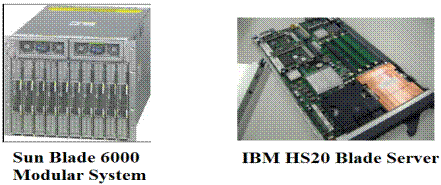
Figure: Blade Enclosure and a Computer
Configured as a Blade Server
Supercomputers: Their Rise, Fall and
Reemergence
High–performance computing has always been of great importance in a
wide variety of scientific and other disciplines. The emphasis on high performance gave rise to
the supercomputer. While there have been
many attempts to give the term “supercomputer” a precise definition, the common
practice is just to equate the term with the list of computers designed and
developed by Seymour Cray, first of the Control Data Corporation and then of
the Cray Computer Corporation (a company he founded).
The
first supercomputer is universally acknowledged to be the CDC–6600, introduced
in 1964; the first unit was delivered to the
Much to the annoyance of the president of IBM, the CDC–6600 was significantly faster than the IBM 7094, up to then the standard machine for scientific computing.
The CDC 6600 is often called the
first RISC (Reduced Instruction Set Computer), due to the simplicity of its
instruction set. The reason for its
simplicity was the desire for speed.
Cray also put a lot of effort into matching the memory and I/O speed with the
CPU speed.
As he later noted, “Anyone can build a fast CPU. The trick is to build a fast system.”
The CDC 6600 lead to the more successful CDC 7600. The CDC 8600 was to be a follow–on to the CDC 7600. While an excellent design, it proved too complex to manufacture successfully, and was abandoned. This feature will be seen again in future designs by Mr. Cray; he simply wanted the fastest machine that could be developed, almost without regard to the practicalities associated with its manufacture.
Cray left Control Data
Corporation in 1972 to found Cray Research, based in
“It boasted a world–record speed of 160 million floating–point operations per second (160 megaflops) and an 8 megabyte (1 million word) main memory. … In order to increase the speed of this system, the Cray–1 had a unique “C” shape which enabled integrated circuits to be closer together. No wire in the system was more than four feet long. To handle the intense heat generated by the computer, Cray developed an innovative refrigeration system using Freon.”
In addition to being the fastest standard computer of its day, the Cray–1 offered a very fast vector processor. The standard processor, by comparison, was called a scalar processor. Most scientific codes of the day made very heavy use of vectors, which are really just groupings of scalars (real numbers, integers, etc.). Consider this FORTRAN code.
DO 100 J = 1, 10
100 A[J] = B[J] + C[J]
This is just a vector addition; the elements of a 10–element vector B being added to those of a 10–element vector C and deposited in a 10–element vector A. Using a standard scalar processor, this would require ten distinct additions. In a vector processor, it essentially required only one addition. This proved a great advance in processing speed.
At over $8 million a copy, the Cray–1 was called the “world’s most expensive love seat”. Note its appearance in the figure below, the low “seats” are really power supplies.
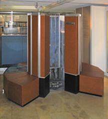
The Cray–1 at the
The fundamental tension at Cray Research, Inc. was between Seymour Cray’s desire to develop new and more powerful computers and the need to keep the cash flow going.
Seymour Cray realized the need for a cash flow at the start. As a result, he decided not to pursue his ideas based on the CDC 8600 design and chose to develop a less aggressive machine. The result was the Cray–1, which was still a remarkable machine.
With its cash flow insured, the company then organized its efforts into two lines of work.
1. Research and development on the CDC 8600 follow–on, to be called the Cray–2.
2. Production
of a line of computers that were derivatives of the Cray–1 with
improved technologies. These were called the X–MP, Y–MP, etc.
The X–MP was introduced in 1982. It was a dual–processor computer with a 9.5 nanosecond (105 MHz) clock and 16 to 128 megawords of static RAM main memory. A four–processor model was introduced in 1984 with a 8.5 nanosecond (118 MHz) clock.
The Y–MP was introduced in 1988, with up to eight processors that used VLSI chips. It had a 32–bit address space, with up to 64 megawords of static RAM main memory. It was the first commercial computer to exceed 1 Gigaflop (109 floating point operations per second), achieving a sustained speed of 2.3 Gigaflops [R54].
While his
assistant, Steve Chen, oversaw the production of the commercially successful
X–MP and Y–MP series, Seymour Cray pursued his development of the Cray–2, a
design based on the CDC 8600, which Cray had started while at the Control Data
Corporation. The original intent was to
build the VLSI chips from gallium arsenide (GaAs), which would allow must
faster circuitry. The technology for
manufacturing GaAs chips was not then mature enough to be useful as circuit
elements in a large computer.
The Cray–2 was a four–processor computer that had 64 to 512 megawords of 128–way interleaved DRAM memory. The computer was built very small in order to be very fast, as a result the circuit boards were built as very compact stacked cards.
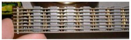
Due to the card density, it was not possible to use air cooling. The entire system was immersed in a tank of Fluorinert™, an inert liquid intended to be a blood substitute. When introduced in 1985, the Cray–2 was not significantly faster than the Y–MP. It sold only thirty copies, all to customers needing its large main memory capacity.
In 1989, Cray
left the company in order to found Cray Computers, Inc. His reason for leaving was that he wanted to
spend more time on research, rather than just churning out the very profitable
computers that his previous company was manufacturing. This lead to an interesting name game:
Cray Research, Inc. producing a large number of commercial
computers
Cray Computer, Inc. mostly invested in research on future
machines.
The Cray–3 was the first project Mr. Cray envisioned for his new company. This was to be a very small computer that fit into a cube one foot on a side. Such a design would require retention of the Fluorinert cooling system. It would also be very difficult to manufacture as it would require robotic assembly and precision welding. It would also have been very difficult to test, as there was no direct access to the internal parts of the machine.
The Cray–3 had a 2 nanosecond cycle time (with a 500 MHz clock). It used Gallium Arsenide semiconductor circuits (with a 80 picosecond switching time), which were five times faster than the silicon semiconductors used in the Cray–2. A single processor machine would have a performance of 948 megaflops; the 16–processor model would have operated at 15.2 gigaflops. A single–processor Cray–3 was delivered in 1993, but the 16–processor model was never delivered. The Cray–4, a smaller version of the Cray–3 with a 1 GHz clock was in development when Cray Computer, Inc. went bankrupt in 1995. Seymour Cray died on October 5, 1996 after an automobile accident.
In the end, the development of traditional supercomputers ran into several problems.
1. The
end of the cold war reduced the pressing need for massive computing facilities.
Some authors have linked the
“computer technology race” to the nuclear arms race.
2. The rise of microprocessor technology allowing much faster and cheaper processors.
3. The rise of VLSI technology, making multiple processor systems more feasible.
Massively
Parallel Processors (MPP)
In the late 1980’s and 1990’s, the key question in high–performance
computer development focused on a choice: use a few (2 to 16) very high
performance processors or a very large number of modified VLSI standard
processors. As Seymour Cray put it: “If
you were plowing a field, which would you rather use: Two strong oxen or 1024
chickens”.
Although Seymour Cray said it more colorfully, there were many objections to the transition from the traditional vector supercomputer (with a few processors) to the massively parallel computing systems that replaced it. The key issue in assessing the commercial viability of a multiple–processor system is the speedup factor; how much faster is a processor with N processors. Here are two opinions from the 1984 IEEE tutorial on supercomputers.
“The speedup factor of using an n–processor system over a uniprocessor system has been theoretically estimated to be within the range (log2n, n/log2n). For example, the speedup range is less than 6.9 for n = 16. Most of today’s commercial multiprocessors have only 2 to 4 processors in a system.”
“By the late 1980s, we may expect systems of 8–16 processors. Unless the technology changes drastically, we will not anticipate massive multiprocessor systems until the 90s.”
Two things
facilitated the introduction of the Massively Parallel Processor systems.
1. The
introduction of fast and cheap processor chips, such as the Pentium varieties.
2. The
discovery that many very important problems could be solved by algorithms
that displayed near “linear
speedup”. Thus, multiplying the number
of processors
by a factor of ten might well
speed up the solution by a factor of nine.
Here is a
picture of the Cray XT–5, one of the later and faster products from Cray, Inc.
[R83]
It is a MPP (Massively Parallel Processor) system, launched in November 2007.
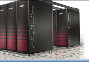
This is built
from a number of Quad–Core AMD Opteron™ processor cores, which are
variants of the Intel Pentium chip. At
least one model of this computer, as well as a MPP model from IBM, have
sustained a speed of 1 Teraflop (1012 floating point operations per
second) on real problems of significance to research scientists. The supercomputer is back.