Overview of
Computer Architecture
The IBM System/360
Edward L.
Bosworth, Ph.D.
TSYS
Department of Computer Science
bosworth_edward@colstate.edu
The Term “Architecture”
The
introduction of the IBM System/360 produced the creation and
definition of the term “computer
architecture”.
According
to IBM [R10]
“The term architecture is used here to
describe the attributes
of a system as seen by the programmer, i.e., the conceptual
structure and functional behavior, as distinct from the
organization of the data flow and controls, the logical design,
and the physical implementation.”
The IBM
engineers realized that “logical structure (as seen by the programmer)
and physical structure (as seen by the engineer) are quite different. Thus, each
may see registers, counters, etc., that to the other are not at all real
entities.”
In more
modern terms, we speak of the “Instruction
Set Architecture”, or
ISA, of a family of computers. This isolates the logical structure of a CPU
in the family from its physical implementation.
In other words, it makes sense to speak of
“programming an IBM S/370”
without specifying the model number.
Architecture, Organization, and
Implementation
The
basic idea behind the IBM System/360 was a family of computers that
shared the same architecture but had different organization.
For
example, each of the computers in the family had 16 general purpose
32–bit registers, numbered 0 through 15.
These were logical constructs.
The
organization of the different models called for registers to be realized
in rather different ways.
Model 30 Dedicated
storage locations in main memory
Models 40 and 50 A dedicated core array, distinct from
main memory.
Models 60, 62, and 70 True data flip–flops, implemented as transistors.
In
general, two models with the same organization will have the same
implementation in hardware.
The
major exception to this is the pair of computers: IBM 709 and IBM 7090.
The
IBM 709 and IBM 7090 share the same organization. The IBM 709 was
implemented with vacuum tubes. The IBM
7090 had the identical organization,
but was implemented with transistors.
Strict Program Compatibility
This was
the driving goal of the common architecture for the IBM S/360 family.
IBM
issued a precise definition for its goal that all models in the S/360 family
be “strictly program compatible”; i.e., that they implement the same
architecture. [R10, page 19].
A family
of computers is defined to be strictly program compatible if and
only if a valid program that runs on one model will run on any model.
There
are a few restrictions on this definition.
1. The
program must be valid. “Invalid programs, i.e., those which
violate the programming manual,
are not constrained to yield
the same results on all models”.
2. The
program cannot require more primary memory storage or types of
I/O devices not available on the
target model.
3. The logic of the program cannot depend on the
time it takes to execute,
unless the program explicitly
tests for event completion.
The smaller models are slower
than the bigger models in the family.
More Design
Goals
Here
are more goals for the S/360 architecture, taken from [R_10].
1. Since computers develop into families, any
proposed design would
have to lend itself to growth and
to successor machines.
2. Storage capacities of more than the commonly
available
32,000 words would be required.
3. Certain types of problems require
floating–point
word length of more than 36 bits.
4. Since the largest servicing problem is
diagnosis of malfunction,
built–in hardware fault–locating
aids are essential to reduce down–times.
5. The general addressing system would have to be
able to refer to small
units of bits, preferably the
unit used for characters.
6. The
design had to yield a range of models with internal performance
“varying from approximately
that of the IBM 1401 to well beyond
that of the IBM 7030 (Stretch)”.
Overview of
Computer Architecture
Each
computer in the IBM S/360 family is a Stored Program Computer, or
“von Neumann Machine”. The top–level
logical architecture is as follows.
Recall
that the actual architecture of a real machine will be somewhat different,
due to the necessity of keeping performance at an acceptable level.
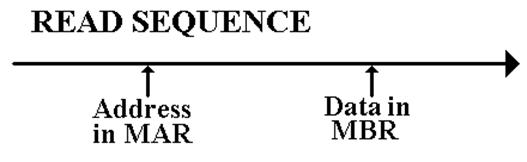
The Fetch–Execute
Cycle
This cycle is the logical basis of all stored program computers.
Instructions are stored in memory as machine language.
Instructions are fetched
from memory and then executed.
The common fetch cycle can be expressed in the
following control sequence.
MAR ¬
PC. // The PC contains
the address of the instruction.
READ. // Put the address into the
MAR and read memory.
IR ¬
MBR. // Place the
instruction into the MBR.
This cycle is described in many different ways, most
of which serve to highlight
additional steps required to execute the instruction. Examples of additional
steps are: Decode the Instruction, Fetch the Arguments, Store the Result, etc.
A stored program computer is often called a “von
Neumann Machine”
after one of the originators of the EDVAC.
This
Fetch–Execute cycle is often called the “von
Neumann bottleneck”, as
the necessity for fetching every instruction from memory slows the computer.
The Dynamic–Static Interface
In order to understand the DSI, we must place it within
the context of a compiler for a
higher–level language. Although most
compilers do not emit assembly language, we
shall find it easier to under the DSI if we pretend that they do.
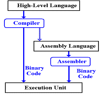
What does the compiler output? There are two options:
1. A very simple assembly language. This requires a sophisticated compiler.
2. A more complex assembly language. This may allow a simpler compiler,
but it requires a more complex
control unit.
The ALU (Arithmetic Logic Unit)
The ALU performs all of the arithmetic and logical
operations for the CPU.
These include the following:
Arithmetic: addition, subtraction, negation, etc.
Logical: AND, OR, NOT, Exclusive OR, etc.
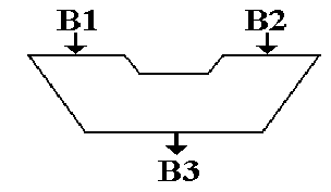
This symbol has been used for the ALU since the mid
1950’s.
It shows two inputs and one output.
The reason for two inputs is the fact that many
operations, such as addition and
logical AND, are dyadic; that is,
they take two input arguments.
For
operations with one input, such as logical NOT, one of the input busses will
be ignored and the contents of the other one used.
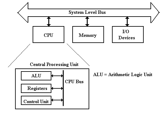
The Central Processing Unit (CPU)
The CPU has four main components:
1. The
Control Unit (along with the IR) interprets the machine language instruction
and issues the control signals to
make the CPU execute it.
2. The
ALU (Arithmetic Logic Unit) that does the arithmetic and logic.
3. The
Register Set (Register File) that stores temporary results related to the
computations. There are also Special Purpose Registers used by the Control Unit.
4. An
internal bus structure for communication.
The
function of the control unit is to
decode the binary machine word in the IR
(Instruction Register) and issue appropriate control signals, mostly to the
CPU.
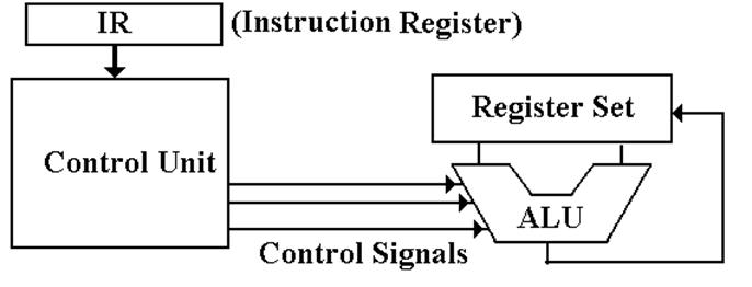
Design of the Control Unit
There are two related issues when considering the
design of the control unit:
1) the complexity of the
Instruction Set Architecture, and
2) the microarchitecture
used to implement the control unit.
In order to make decisions on the complexity, we must
place the role of the control unit
within the context of what is called the DSI
(Dynamic Static Interface).
The ISA (Instruction Set Architecture) of a
computer is the set of assembly language
commands that the computer can execute.
It can be seen as the interface between the
software (expressed as assembly language) and the hardware.
A more complex ISA requires a more complex control
unit.
At some point in the development of computers, the
complexity of the control unit
became a problem for the designers. In
order to simplify the design, the developers of the
control unit for the IBM–360 elected to make it a microprogrammed unit.
This
design strategy, which dates back to the Manchester Mark I in the early 1950’s,
turns the control unit into an extremely primitive computer that interprets the
contents
of the IR and issues control signals as appropriate.
The Micro–Programmed
Control Unit
In
a micro–programmed control unit, the control signals correspond to bits in a
micro–memory, which are read into a
micro–MBR and emitted.
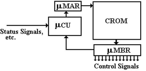
The micro–control unit ( mCU )
1) places
an address into the micro–Memory Address Register ( mMAR ),
2) the
control word is read from the Control Read–Only Memory (CROM),
3) into
the micro–Memory Buffer Register, and
4) the
control signals are issued.
The Micro–Programmed Control Unit
The goal of the System/360 micro–programmed control
unit [R_51] was to “help
design a fixed instruction set capable of reaching across a compatible line
of machines in a wide range of performances”.
The same authors [R_51] go on to note that “the use of
microprogramming
has, however, made it feasible for the smaller models of SYSTEM/360 to
provide the same comprehensive instruction set as the larger models”.
Tucker [R_51] notes that “There has been much talk,
but little success, in
providing higher–level languages for micro–programs. There seem to be a
number of factors which contribute to this.
Primarily, almost no inefficiency
is tolerated in micro–programs”.
Tucker goes on to speak of the “micro–programmer who
can justifiably spend
hours trying to squeeze a cycle out of his code and who may make changes
to the data path to do so”.
Tucker notes that the System/360 Model 30 is
micro–programmed to run
IBM 1401 programs in their native form.
This was an additional inducement
to those owning an IBM 1401 to “move up”.
Handling Legacy Software
During the introduction of the System/360, IBM
underestimated the large customer
investment in legacy software especially at the assembly language level.
In order to prevent mass defection of customers to
Honeywell, which was offering its
model H–200 that would run IBM 1401 assembly language programs, IBM was forced
to develop some sort of simulator to run on the System/360.
It was understood that a software simulator of the IBM
1401 running on any System/360
model would be unacceptably slow.
IBM was “spared mass defection of former customers”
when engineers working on the
Model 30 suggested the use of an extra control store on the micro–programmed
control
unit to allow the Model 30 to execute IBM 1401 instructions in native mode
[R_62].
Stuart Tucker and Larry Moss led the effort to provide
the ability on the System/360
Model 30 to execute native mode software for both the IBM 1401 and IBM 700
series.
Moss termed their work as “emulation”
[R_63].
The emulators they designed worked well enough so that
many customers never
converted legacy software and instead ran it for many years on System/360
hardware using emulation. This was a
great marketing success for IBM.
The Register
File
There are two sets of registers, called “General
Purpose” and “Special Purpose”.
The origin of the register set is simply the need to
have some sort of memory on the
computer and the inability to build what we now call “main memory”.
When reliable technologies, such as magnetic cores,
became available for main memory,
the concept of CPU registers was retained.
Registers are now implemented as a set of flip–flops
physically located on the CPU chip.
These are used because access times for registers are two orders of magnitude
faster than
access times for main memory: 1 nanosecond vs. 80 nanoseconds.
General
Purpose Registers
These are mostly used to store intermediate results of
computation. The System/360
architecture calls for sixteen 32–bit registers, numbered 0 through 15. While these
might be called “general purpose”, a few of the registers have dedicated uses.
Registers 0
and 1 can be used as temporary
registers, but calls to supervisor routines
will destroy their contents. Register 0 cannot be used as a base
register or index register.
Register 2 can be used as a temporary and possibly as a base
register.
The TRT (Translate and Test) instruction will change the value of this
register.
Registers 13, 14, and 15 are used by the control programs and subprograms.
More on the
General Purpose Registers
There are two important concepts discussed in the
previous slide.
1. That only registers 3 through 12 of the
sixteen registers are to be viewed
as truly general purpose.
2. That the use of some hardware resources
evolves by consent of the software
designers. There is nothing in the hardware architecture
that restricts the
use of registers 0, 1, 13, 14,
and 15.
The
restricted use of these registers is a design decision by the system
programmers to facilitate the
design of system software.
These ten registers, R3 – R12, can be used for binary
integer arithmetic, and for
the computation of the effective address of a memory storage element.
The System/360 and subsequent machines use
base–displacement addressing with
an optional indexing.
The index value is stored in the index register, a
general purpose register that
is being used as an index. We shall
discuss indexing later.
A base address is stored in the base register, a
general purpose register that
is being used as the base register. We
shall discuss base registers later.
The Register
File
Special
Purpose Registers
These are often used by the control unit in its execution
of the program.
IR the Instruction
Register. This holds the machine
language version of
the instruction currently
being executed.
MAR the Memory
Address Register. This holds the
address of the memory word
being referenced. All execution steps begin with PC ® MAR.
MBR the Memory
Buffer Register, also called MDR (Memory Data Register).
This holds the data being
read from memory or written to memory.
PSW the Program
Status Word, contains a collection of logical bits that
characterize the status of
the program execution.
Bit
12 of the PSW is the ASCII bit; the S/360 will use ASCII if this is set.
The feature was never
used; in the S/370 and later it has another meaning.
PC the Program
Counter, so called because it does not count anything.
It is also called the IP (Instruction Pointer), a much better
name.
The PC points to the
memory location of the instruction to be executed next.
The System/360 architecture
calls for this to be stored in the 24 low–order
bits of the 64–bit PSW.
Design
Decisions: The Data Format
Apparently, there were two main options for the size
of the basic storage cell.
2N the size would be 4, 8, 16, 32, or 64
bits.
3·2N the
size would be 6, 12, 24, or 48 bits.
Character size, 6 vs. 4/8
At the time, the character set of existing IBM
computers comprised 64 characters,
inherited from the punch card codes of the day.
Decimal digits required 4 bits to encode; general
alphanumeric characters required 6 bits.
On option was to use 6 bits to encode everything. This wasted 2 bits for each
encoding of a decimal digit.
Another option was 4 bits for digits and 8 bits for
alphanumeric characters,
thus wasting 2 bits for every alphanumeric character.
The option of 4 bits for digits and 6 bits for
alphanumeric characters would require the
basic addressable unit to be a multiple of 12 bits. This was thought overly complex.
In the end, all of the “6 options” were rejected,
because the designers realized that
committing to a 6–bit character encoding was “short–sighted” [R_10].
IBM 029
Punch Card Codes
Here is a card punched with
each of the 64 characters available under this format.
Note the lack of lower case letters; the IBM Mainframe assembler reflects this.
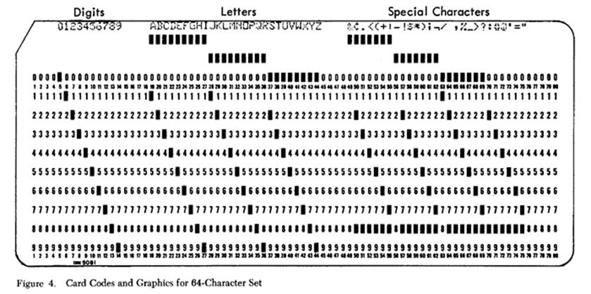
This
is the complete set of characters to which the designers thought it would be
“short sighted” to commit. They held out
for a larger character set.
Data Types
We must recall that, in the world of the IBM
System/360, there are three
major classes of numeric data.
1. Binary
Integer Data.
This
format calls for use of two’s–complement binary integers, in
lengths of 16 or 32 bits.
A
variant used in addressing calls for 12–bit unsigned integers.
2. Packed
Decimal Data
This
is also called “decimal data”. It calls
for the use of (N + 1) hexadecimal
digits to store an N–digit
decimal number in (N + 1)/2 bytes.
Remember
that N must be an odd integer.
I use
the term “fixed point” to reference data of this sort. IBM occasionally seems
to expand the term “fixed point”
to include binary integer data.
3. Floating
Point Data
These
are real numbers without a fixed decimal point.
Floating–Point
Arithmetic
Earlier IBM models had used 48–bit representations of
all floating–point numbers.
The choice for the S/360 family was narrowed to two
options [R_10]:
1. One representation based on the use of 48
bits.
2. Two representations: 32 bits (single
precision) and 64 bits (double precision).
The article noted a lack of experimental data on the
required precision.
IBM decided to offer both single precision and double
precision.
The IBM System/370 apparently introduced a third
format, extended precision.
The rationale for the choice is stated in [R_10].
“The user of the large models is expected to employ
64–bit words most
of the time. The user of the smaller
models will find the 32–bit length
advantageous in most of his work. All
floating–point models have
both lengths and operate identically”.
We shall study the details of the two floating–point
implementations at a later time.
Integer Arithmetic
As we shall see later, the IBM System/360 provides for
two integer sizes:
half words (16 bits) and full
words (32 bits).
The designers had to choose the method for
representing negative integers.
The two’s–complement method was chosen.
In addition to the obvious advantage of a single
representation of zero, the
designers make a number of claims for the superiority of two’s–complement.
1. Its utility in address arithmetic,
“particularly in the large models, where
address arithmetic has its own
hardware” rather than sharing the ALU.
2. The simplification of the indexing hardware
for address computations.
3. The claim that the smaller models, which used
bit–serial arithmetic,
would compute more efficiently
with two’s–complement integers.
4. The fact that conversion from floating–point
to integer representation
involves
“truncation … in the same direction”.
Decimal Data
The
choice of format for decimal data is explained as follows [R_10],
“The established commercial rounding convention made
the use
of complement notation awkward for decimal data; therefore,
absolute–value–plus–sign is used here”.
As we have seen, the hexadecimal digit D is used for negative
numbers and
the hexadecimal digit C for non–negative numbers.
As
opposed to binary integer data, which comes in fixed sizes, the designers
of the System/360 opted for variable–length decimal fields.
“Since the fields of business records vary
substantially in length,
coding efficiency (and hence tape speed, file capacity, CPU speed, etc.)
can be gained by operating directly on variable–length
fields”.
Note the concern for speed in reading data from
magnetic tapes.
The designers noted that a fixed–length format might
be preferable for larger models
in the series, as they would be expected to have a greater memory capacity.
The designers give two reasons for the choice of
variable–length format.
1. The
small commercial users would expect the format, and
2. The
larger systems are usually I/O limited, so the decreased CPU efficiency
does not present a bottleneck.
Decimal
Accumulators vs. Storage–To–Storage Operations
The System/360 family architecture provides a set of
registers for integer data.
The designers then faced the option of creating a
special register set for decimal
data. Note that the 32–bit (4 byte)
general purpose registers would not work, as
they would limit the decimal numbers to seven digits each.
The packed decimal format specified for the System/360
and later calls for no
more than 31 decimal digits (16 bytes) in the Packed Decimal Format.
One choice would be to create a number of 128–bit (16
byte) registers specifically
for packed decimal arithmetic. The
article calls these “decimal
accumulators”.
There are a number of reasons cited for the decision
not to use decimal accumulators.
1. “For the smaller model, using core storage for
local registers, addition to an
accumulator is no faster than
addition to a programmer–specified location”.
2. In the decimal accumulator model, “addition of
two arbitrary operands and
storage of the result becomes
LOAD, ADD, STORE, however, and this
operation is substantially slower
for the smaller models than the MOVE ADD
sequence appropriate to
storage–storage operation”.
3. Business arithmetic “rarely occur
in strings [sequences of execution] where
intermediate results are
profitably held in accumulators”.
ASCII vs.
EBCDIC
It is a little–known fact that the early System/360
models could be run in either
ASCII or EBCDIC mode. As it was very
rare, the ASCII mode has been dropped.
The designers of the System/360 give some good reasons
against “the adoption of
ASCII as the only internal code for
System/360”.
To
quote the designers of the System/360
“The reasons against such exclusive adoption was the
widespread use of the
BCD code derived from and easily translated to the IBM [029] card code”.
Note that they argue only against the exclusive
adoption of ASCII.
Consider the IBM 029 punch
codes and compare them to the EBCDIC.
|
Character |
EBCDIC |
Punch Card Codes |
|
0 through 9 |
F0 through F9 |
0 through 9 |
|
A through I |
C1 through C9 |
12–1 through 12–9 |
|
J through R |
D1 through D9 |
11–1 through 11–9 |
|
S through Z |
E2 through E9 |
0–2 through 0–9 |
Memory
Timings
Memory Access Time
Defined in terms of reading from memory. It is the time
between the address
becoming stable in the MAR and the data becoming available in the MBR.
Memory Cycle Time
Less
used, this is defined as the minimum time between two independent
memory accesses.
Two Components of Memory Timings
These are 1) the time to
decode the memory address so that the correct cell is
addressed, and 2) the time to access the addressed cell.
The
System/360 Memory Descriptions
This table shows the range of memory capacities and
performance found in
the original family of the System/360.
In this table, memory performance is characterized by cycle time, which is the
minimum time between two independent writes to the same memory unit.
|
Model |
Capacity |
Actual
Memory |
Cycle Time |
|
30 |
8 to 64 KB |
8 bits |
2.0 msec |
|
40 |
16 to 256 KB |
16 bits |
2.5 msec |
|
50 |
32 to 256 KB |
32 bits |
2.0 msec |
|
60 |
128 to 512 KB |
64 bits |
2.0 msec |
|
62 |
256 to 512 KB |
64 bits |
1.0 msec |
|
70 |
256 to 512 KB |
64 bits |
1.0 msec |
Consider
the fact that the Assembler had to be run on a System/360 – Model 30.
This
required that the Assembler execute in a very small amount of memory.
As
a result, the Assembler is not very sophisticated, and the structure required
of standard assembly language programs is rather rigid.
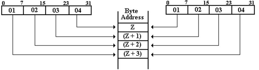
Word
Addressing in a Byte Addressable Machine
Each
8–bit byte has a distinct address.
A
16–bit half–word at address Z contains bytes at addresses Z and Z + 1.
A
32–bit full–word at address Z contains bytes at addresses
Z, Z + 1, Z + 2, and Z + 3.
Note
that assembly language refers to addresses, rather than variables. We just
pretend to be handling variables; these are a construct of high–level
languages.
There
are two strategies for storing a multiple–byte entry in a byte–addressable
computer. Following a story in
Gulliver’s Travels (not a children’s book),
we call these strategies “Big Endian” and “Little Endian”.
The
IBM System/360 assembler (the two variants are called “Assembler H”
and “HLASM”) will align all data storage as follows:
16–bit half words are stored at even
addresses,
32–bit full words are stored at addresses
that are multiples of 4, and
64–bit double words are stored at
addresses that are multiples of 8.
Big–Endian vs. Little–Endian
Addressing
The
value in the register is 0x01020304; in IBM notation
it is X’01020304’.

Address Big-Endian Little-Endian
Z 01 04
Z + 1 02 03
Z + 2 03 02
Z + 3 04 01
Example:
“Core Dump” at Address 0x200
Note: Powers of 256 are 2560 = 1, 2561
= 256,
2562
= 65536, 2563
= 16,777,216
Suppose
one has the following memory map as a result of a core dump.
The memory is byte addressable.
|
Address |
0x200 |
0x201 |
0x202 |
0x203 |
|
Contents |
02 |
04 |
06 |
08 |
What is the value of the
32–bit long integer stored at address 0x200?
This is stored in the
four bytes at addresses 0x200, 0x201, 0x202, and 0x203.
Big
Endian: The
number is 0x02040608.
Its decimal value is
2·2563 + 4·2562 + 6·2561 + 8·1 = 33,818,120
Little
Endian: The
number is 0x08060402.
Its decimal value is
8·2563 + 6·2562 + 4·2561 + 2·1 = 134,611,970.
NOTE: Read the bytes backwards, not the hexadecimal
digits.
Example 2:
“Core Dump” at Address 0x200
Note: Powers of 256 are 2560 = 1, 2561
= 256,
2562
= 65536, 2563
= 16,777,216
Suppose
one has the following memory map as a result of a core dump.
The memory is byte addressable.
|
Address |
0x200 |
0x201 |
0x202 |
0x203 |
|
Contents |
02 |
04 |
06 |
08 |
What is the value of the
16–bit integer stored at address 0x200?
This is stored in the
two bytes at addresses 0x200 and 0x201.
Big
Endian The
value is 0x0204.
The decimal
value is 2·256 + 4 = 516
Little
Endian: The
value is 0x0402.
The decimal
value s 4·256 + 2 = 1,026
Note: The bytes at addresses 0x202 and 0x203 are not part of this
16–bit integer.
Input/Output
System
The
System/360 designers opted for a uniform logical
architecture for I/O and
not for a uniform method of implementation.
The
smaller models were designed to use the CPU hardware for I/O functions.
The
larger models were designed to use independent execution units, called
“I/O Channels” for I/O. Each I/O Channel could operate concurrently
with the
CPU and with any other I/O Channel.
The
designers note that “such large–machine channels often each contain
more components than an entire small system”.
The
System/360 architecture calls for the Channel to be an independently
operating entity, without regard to its actual implementation.
The
CPU creates a “channel program”, which comprises a small number of
“channel commands” (SEARCH, READ, WRITE, or READ FOR CHECK).
In
the smaller System/360 models, the Channel is a logical device, and “the flow
of data and control information is time–shared between the CPU and the channel
function”. The Channel is viewed as a
“conceptual entity”.
On
the larger systems, the Channel is implemented with distinctly separate
hardware.
The
System/360 Model 40 from 1964
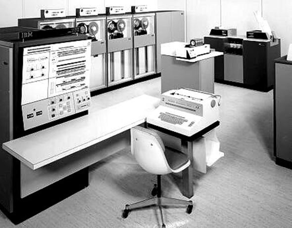
This
is a picture of one of the original S/360 smaller models.
The
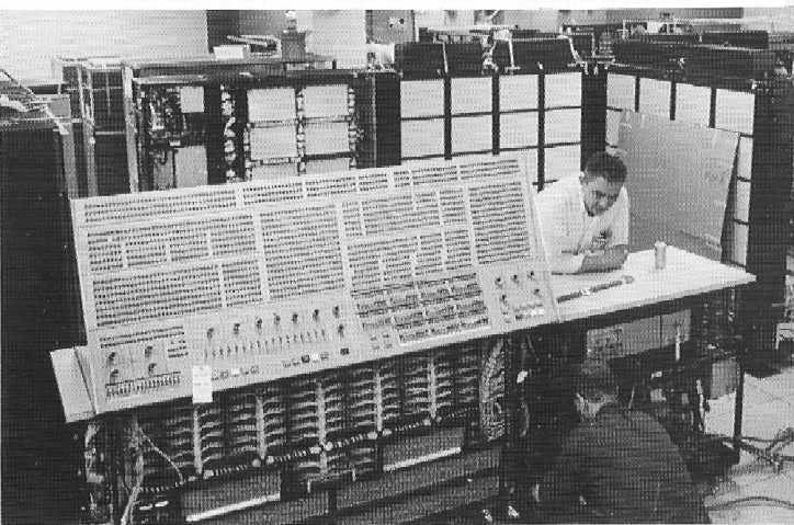
System/360 Model 91 from 1968
I
believe that this model is the largest S/360 built. It was rated at 16.6 MIPS.
The
System/360 Model 91 from 1968
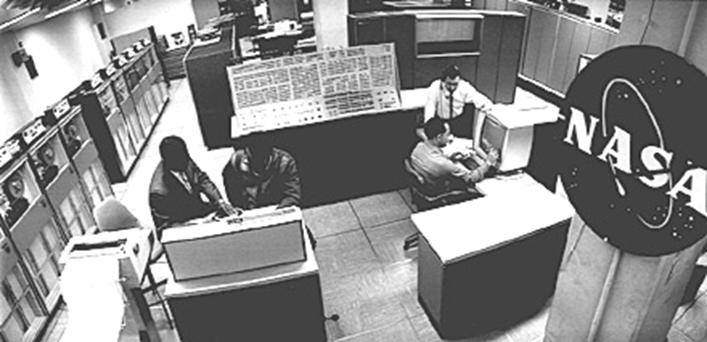
This
is a Model 91 at NASA’s Goddard Space Flight Center
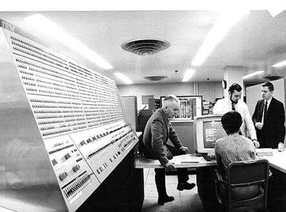
Installing a
System/360 Model 91
This
shows a 1969 installation at
A Smaller
S/360: The Model 22 in 1971
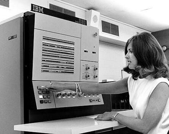
Again,
note the omnipresent control panel.
A Typical
System/370 Installation
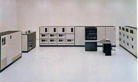
Note
the large number of disk drives.
The Z–Series
990
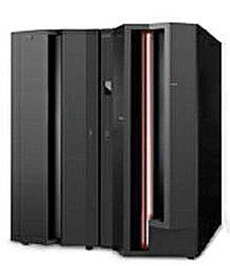
The
machine we run on probably looks like this one.
References
NOTE: The reference numbers in this set of slides
are those from the
original textbook. For that reason, they are out of order.
R_11 Mark D. Hill, Norman P. Jouppi, & Gurindar S. Sohi, Readings in Computer
Architecture, Morgan
Kaufmann Publishers, 2000, ISBN 1 – 55860 – 539 – 8.
R_10 G. M. Amdahl, G. A. Blaauw,
& F. P. Brooks, Architecture of the IBM
System/360, IBM Journal of
Research and Development, April 1964.
Reprinted
in R_11.
R_12 D. W.
Model 91: Machine
Philosophy and Instruction–Handling,
IBM Journal of Research and
Development, January 1967. Reprinted in R_11.
R_46 C. J. Bashe, W.
Buchholz, et. al., The Architecture of IBM’s Early
Computers, IBM J. Research
& Development, Vol. 25(5),
pages 363 – 376, September
1981.
R50 P. M. Davies,
(Number
1), pages 16 – 40.
R_51 S. G. Tucker, Microprogram
Control for System/360, IBM Systems Journal,
Volume
6, No. 4 (1967), pages 222 – 241.
R_62 M.A. McCormack, T.T. Schansman,
and K.K. Womack, “1401 Compatibility
Feature
on the IBM System/360 Model 30,” Communications of the ACM,
v.
8, n. 12, 1965, pp. 773-776.
R_63
S.G. Tucker, "Emulation of
Large Systems," Communications of the ACM,
v. 8, n. 12, 1965, pp.
753-761.
Web Sites of Interest
R_45 http://www–03.ibm.com/ibm/history/exhibits/
R_41 http://www.columbia.edu/acis/history/