On the other
hand, the IBM System/360 was designed as a general–purpose computer, with
emphasis on commercial calculations.
Among the data types supported were:
Signed integers, both 16–bit
and 32–bit,
Character data, using the IBM
EBCDIC scheme,
Floating point numbers:
single–precision, double–precision, and extended precision, and
Packed decimal data types for
commercial computation.
Some data types
are mistakes and some are a bit strange.
The early PDP–11 supported a 16–bit
floating point standard that provided so little precision as to be
useless. It was quickly dropped.
Some of the LISP machines (designed to execute the LISP language) supported bignums, which
are integers of unbounded size. A
typical computation using bignums would be to compute
the value of the mathematical constant p to 100,000
decimal places.
The 8–bit byte was created by IBM for use on the
System/360. It was designed to hold an
EBCDIC character. At the time, only
seven bits were required for the character set, but IBM
wisely chose to extend the encodings to eight bits. For some time later, it was assumed that
the term “byte” was trademarked by IBM, so the early Internet designers
referred to a grouping
of eight bits as an octet. The term has stuck in the network world;
others call it a byte.
There are a
number of possible data types that generally are not supported by any
computer.
One silly example is the Roman Number system.
This is nothing more than a different print
representation of positive integers; the decimal number 64 would be printed as LXIIII. In
other words, this is not a candidate for a data type.
Complex numbers,
of the form x + iy, where i is the square root of
–1, are candidates for a
data type. The number would be stored as
a pair of real numbers (x, y), and be processed by
the CPU according to the rules of complex arithmetic; e.g., (x1,
y1)
+ (x2,
y2)
= (x1
+x2,
y1
+y2).
The uniform choice has been to implement the real number arithmetic in a special
floating point
unit, but to implement the complex arithmetic itself in software.
Fixed–length vs.
Variable–Length Instructions
A stored program
computer executes assembly language instructions that have been converted to
binary machine language. In all modern
computers, the length of each instruction is a multiple
of 8 bits, so that the complete instruction occupies an integral number of
bytes.
Some modern
computers are designed to have a fixed instruction length. At the moment, the
most common length is 32 bits or four bytes.
This allows a simpler control unit for the CPU,
but does have some penalties in memory usage.
Computer organizations devised in the 1960’s
and 1970’s tend to have variable length instructions and slightly more complex
control units.
The use of variable length instructions makes better use of computer memory,
which before
about 1980 was a costly asset. Here are
some cost data for one megabyte of memory.
In 1970
one megabyte would cost about $730,000.
In 1979 one megabyte cost about $6,700.
In 1990,
the cost was $46.00. In 2000, the cost
per megabyte was seventy cents, assuming that one could
buy such a small memory.
Perhaps the most
common example of an organization is that of the Pentium series. This has to
do with the early history of the Intel IA–32 line and the later desire to
maintain compatibility
with the early models. The origins of
the design come from the 8–bit Intel 8080, designed in
the early 1970’s and released in April 1974.
The next subchapter of this textbook will cover
the evolution of the Intel computer line.
In order to
illustrate the memory usage problems associated with fixed length instructions,
we
shall first examine two designs, each with fixed–length 32–bit instructions. These are the
Boz–7 (a hypothetical design by the author of this textbook) and the MIPS, a
real device in
use for many game controllers and other hardware.
The Boz–7 has
one format that calls for 32–bit machine language instructions for all assembly
language statements. The standard calls
for a five–bit opcode (used to identify the operation).
|
Bit |
31 |
30 |
29 |
28 |
27 |
26 |
25 – 0 |
|
Use |
5–bit opcode |
Address Modifier |
Use depends on the opcode |
||||
Here are a few instructions, with comments.
The
halt instruction has opcode 00000, or decimal
0. It stops the computer.
|
Bit |
31 |
30 |
29 |
28 |
27 |
26 |
25 – 0 |
|
Use |
00000 |
Not used |
Not used |
||||
Note that 27 of the 32 bits in this binary
instruction are not used. Given the
reasonable
requirement that the instruction length be a multiple of 8, it would be very
easy to package this
as a single byte, if the instruction set supported variable length
instructions; a 75% saving.
The standard
arithmetic instructions, such as ADD and SUB have this format. This figure shows
a subtract instruction SUB R5, R6, R4, setting register R5 = R6 – R4.
|
31 |
30 |
29 |
28 |
27 |
26 |
25 |
24 |
23 |
22 |
21 |
20 |
19 |
18 |
17 |
16
– 0 |
|
10110 |
0 |
101 |
110 |
100 |
Not
used |
||||||||||
Here, only 17 of the 32 bits are not used. Instructions of this type could easily be
packaged
in two bytes, leading to a 50% saving in memory usage.
Only the two
memory access instructions (LDR – load register from memory, STR – store
register into memory), the branch instruction, and the subroutine call
instruction use the full
32 bits allocated for the instruction format.
The Boz–7 is designed as a didactic
computer,
focusing on the teaching of basic concepts; it has never been built and never
will be.
The MIPS (Microprocessor without Interlocked Pipeline Stages) is a
real commercial computer
with fixed–length binary instructions of 32 bits. It was developed in the early 1980’s by a
team
that included one of the authors (John L. Hennessy) of the reference [R007]
used to describe it.
The first product, the R2000 microprocessor, was shipped in 1986.
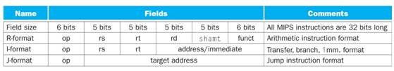
The MIPS core
instruction set has about 60 instructions in three basic formats. All instructions
are 32 bits long, with the most significant six bits representing the opcode. The MIPS design
employs an interesting trick; many arithmetic operations have the same opcode,
with the
function selector, funct, selecting
the function. Addition has opcode = 0
and funct = 32.
Subtraction has opcode = 0 and funct = 34.
This makes better use of memory.
The IBM System/360
The IBM
System/360 comprises a family of similar computers, designed in the early 1960’s,
announced on April 7, 1964, and first sold in mid 1965. The smallest model, the S/360–20
had only 4 KB (4,096 bytes) of main memory.
Many of the larger models were shipped with
only 128 KB to 512 KB of main memory.
For this reason, the S/360
instruction set provides for instruction lengths of 2 bytes, 4 bytes, and
6 bytes. This resulted in six
instruction classes, each with an encoding scheme that allowed the
maximum amount of information to be specified in a small number of bytes. All instructions
in the ISA have an 8–bit (one byte) opcode.
These formats are classified by
length in bytes. The five common instruction
classes of use
to the general user are listed below.
Format Length Use
Name in
bytes
RR 2 Register to register
transfers.
RS 4 Register to storage and
register from storage
RX 4 Register to indexed storage
and register from indexed storage
SI 4 Storage immediate
SS 6 Storage–to–Storage. These have two variants.
The AR
instruction is typical of the RR format.
The S/360 had 16 general–purpose registers,
requiring 4 bits (one hexadecimal digit) to identify. The machine language translation of this
instruction requires 16 bits (two bytes): 8 bits for the opcode and 4 bits for
each register.
The opcode for AR is 1A. Here
are some examples of machine code.
AR 6,8 1A 68 Adds the contents of
register 8 to register 6.
AR 10,11 1A AB Adds
the contents of register 11 to register 10.
A reasonable
estimate of the average length of a machine instruction in a typical job mix
would
be a bit more than 4 bytes. This is a
33% saving over the requirement for 6 bytes per machine
language instruction, were uniform length instructions used.
As the IBM
mainframe series evolved, the company maintained strict binary program
compatibility. New series started with
the System/370 in the 1970’s, continued through to
the z/Series in the 2000’s and now the z/Enterprise models. When your author teaches IBM
assembly language, he assigns programs in System/370 assembly language to be
run on an
IBM z/9, announced on July 25, 2005 and first shipped on September 16,
2005. These always
run without any difficulty, once the students get the coding correct.
The Intel Pentium
The Pentium
instruction set architecture is considerably more complex than even the IBM
System/360. This design may be said to
support variable length machine language instructions
with a vengeance; the instruction length can vary from 1 through 17 (possibly
15) bytes.
We shall discuss the details of the Pentium ISA in chapter 7C, after first
discussing the evolution
of the IA–32 architecture from the early 8–bit designs, through the 16–bit
designs, and officially
starting with the Intel 80386, the first 32–bit design. That discussion will be in chapter 7B.
Instruction Types
There
are basic instruction types that are commonly supported.
1. Data Movement (Better called “Data
Copy”) These copy data from a source
to a
destination. Suppose that X and Y are 32–bit real numbers
at fixed memory locations.
The instruction Y = X makes a copy
of the four bytes associated with X and places them
in the four bytes at the address
for Y. The value at the address for X is
not changed;
nothing is “moved out”.
2. Arithmetic The standard arithmetic operators are usually
supported. It might
come as a surprise that a
modern CPU can support only the four standard arithmetic
operations: addition, subtraction, multiplication, and
division. Some early designs did
not support either
multiplication or division. If division
is supported, one usually also has
the mod and rem functions. On business–oriented machines, decimal
arithmetic is
always supported, being immune
to the round–off problems of floating point arithmetic.
Graphics–oriented machines
usually support saturation arithmetic,
in which a sum that
exceeds the maximum allowable
is set to the maximum. For example,
unsigned 8–bit
arithmetic can support
integers only in the range 0 through 255, inclusive. In standard
arithmetic, the sum 200 + 200
could not be represented; it would cause an overflow.
In saturation arithmetic, we
set 200 + 200 arbitrarily to 255, the maximum value.
Real number arithmetic is often not
handled directly in the CPU, but by a coprocessor
attached to it. Early on (Intel 80486 / 80487) this was a
cost consideration.
RISC machines follow this
approach in order to keep the CPU simple.
3. Boolean Logic There are two standard classes of Boolean type
instructions. The
more common involves the
standard Boolean functions AND, OR, NOT, and XOR.
These are described in chapter
4 of this textbook.
4. Bit Manipulation These use instructions that appear to be Boolean, but in fact
operate differently. This is a distinction lost on many students, perhaps
because it is
rarely important. Here are some examples of bitwise operations. These operations
are often used to set Boolean
bit flags in device control registers.
1001 0110 1001 0110 1001 0110
AND 1100 0011 OR 1100
0011 XOR 1100 0011
1000 0010 1101 0111 0101 0101
5. Input / Output The computer must communicate with external devices, including
permanent storage, printers
and keyboards, process control devices (through dedicated
I/O registers), etc. All commercial machines have “addressable”
I/O devices; i.e., the
CPU issues a device identifier
that appears to be an address to select the device. From
the CPU viewpoint, each I/O
device is nothing more than a set of registers (control,
status, and data) and some
timing constraints.
6. Transfer of Control These alter the normal sequential execution of
code. At the
primitive machine language
level, all we have is unconditional jumps, conditional jumps,
and subroutine
invocations. Higher level languages
elaborate these features with
constructs such as conditional
statements, counted loops, and conditional loops.
The Basic Instruction Set Design
At first, this
seems to be a strange question. Don’t
all computers do the same thing? The
answer
is that the instructions chosen depend on what the computer is to do. For example, a computer
designed to be a router in the global Internet will function almost exclusively
as a data router,
moving bytes from one data buffer to another.
It has little use for floating–point arithmetic. If
the addition of floating–point to the CPU will slow it down, that feature will
be omitted.
Most students
relate to computers on a simple, but important, basis: “Here is the computer,
here
is what it does, just use it”. It is
worth note that some person or group of persons had to design
that computer, which means designing the CPU, which means designing the ISA
(Instruction Set
Architecture). Most new designs begin
with a list of desired features and move through a series
of compromises focusing on what can be delivered at reasonable price and
performance. We use
the ENIAC as an obvious example. When
designed in the early 1940’s it had no memory as we
would recognize it. The reason that the
designers chose not to have even a modestly sized
memory was cost. A 128 KB memory would
have cost millions of dollars. Moreover,
it would
have used about one million vacuum tubes, which were in short supply due to the
war. One of
the ENIAC developers reported that the team used whatever tubes it could find
in the design of
the arithmetic logic unit for the machine.
Here are some of the design issues involved in
the creation of a new CPU.
The
number and names of the registers.
A register is considered to be a
short–term memory device associated with the CPU. In this, it
differs from the memory component, which is considered as being separate from
the CPU. After
we discuss the Pentium ISA and then discuss the multi–level cache memory
associated with the
Pentium chips, we shall see that the real difference between a register and a
primary memory
location is the use made of it by the assembly language. A modern Pentium design is likely to
have a few megabytes of cache memory on the CPU chip; this blurs the physical
distinction
between registers and memory.
Early computer
designs favored very few registers, primarily because the technology used to
create register memory was both expensive and prone to failure. In fact, some early designs
(such as the PDP–1 and IBM S/360–20) treated registers as logical concepts,
actually using
dedicated memory locations to serve as registers.
The earliest
machines to have registers were single
accumulator machines, with one general
purpose register used to accumulate the results. This design is still seen in the many
calculators
that use a single display line to show the results; this display reflects the
contents of a single
register that might be called the accumulator.
For an introduction to this type of device, the
reader is invited to examine the MS–Windows Calculator.
The next step in
the evolution was the two–register machine.
One early example of this design
was the PDP–9, first manufactured in 1968.
These two registers, called the AC
(Accumulator)
and the MQ (Multiplier–Quotient),
used as an extension of the accumulator to more easily
handle integer multiplication and division.
Beginning in the
mid 1960’s, most computers were designed with multiple general–purpose
registers. The IBM S/360 series is
typical of the time; this design provided sixteen registers
labeled 0 through 15. As noted above,
these registers were a logical construct.
In the cheaper
models the registers were dedicated memory locations, in others a separate
memory. Only in
the faster, and more expensive, units were the registers implemented with
flip–flops.
The PDP–11,
designed in the late 1960’s, provided eight registers, labeled 0 through
7. The
VAX–11 series, designed in the late 1970’s provided 16 registers, labeled 0 through
15. The
MIPS, designed in the early 1980’s, provided 32 registers, 0 through 31. Other designs, such as
the SPARC, offered even more registers.
Today, 32 general–purpose registers are common.
The one strange
design is part of a series that began with the Intel 8080, released in
1974. This
evolved gradually into the Pentium series.
The original 8080 had seven 8–bit general purpose
registers (A, B, C, D, E, H, and L) as well as two special purpose registers (W
and Z) to hold
temporary results. The A register was
the accumulator and the other six often had dedicated
uses that occasionally prevented their use for general computations. These six could be treated
as three pairs (BC, DE, and HL) in order to process 16–bit results.
The evolution of
this register set into the modern Pentium set will be covered in the next
sub–chapter. Here, we just note that the
Intel 8080 set the roadmap for all others in the series.
Floating
point
Some early
computer designs provided hardware support for floating–point arithmetic, and
some
did not, mostly due to the complexity and cost of the FPU (Floating–Point Unit). All computers
in the IBM mainframe series, beginning with the System/360 provided hardware
support for
floating–point as an integral part of the CPU.
The PDP–9, from about the same time, did not
offer hardware support, but emulated floating–point arithmetic in
software. Your author has
written a floating–point emulator for the PDP–9 that used only integer
arithmetic instructions;
to say that it was very slow is to be quite generous.
Again, the
decision on floating–point arithmetic was based on the expected use. Those designs
dedicated to message switching and device control probably did not have any
implementation.
Those designed to support scientific computation required a fast hardware
implementation; a
supercomputer without floating–point is about as useful as a car without
wheels.
In general, the
standard FPU provides the basic operations: addition, subtraction,
multiplication,
and division. It is worth note that
Seymour Cray, the developer of the CDC–6600 and Cray –1,
was so obsessed with performance that he replaced division with an inverse
operator. In order to
compute Y/X, it first computed (1/X) and then multiplied to get Y/X = Y·(1/X).
The Intel series
of microprocessors chose another route for floating–point arithmetic. It appears
that the early members of the sequence (8080, 8086, and 8088) did not provide
for floating point,
and that a separate floating point unit, the Intel 8087, was designed to fill
the bill.
The Intel 8086
was a 16–bit processor introduced in 1978.
The Intel 8088 was a simpler, and
cheaper, variant of the Intel 8086. The
Intel 8087, introduced in 1980, was designed as a
separate chip, called a “floating point coprocessor”. Because the Intel 8087 was a new design
intended to be a separate chip, its organization was not constrained by the
Intel 8086 register set.
As a result, a rather interesting 80–bit floating–point format was designed and
implemented on
the Intel 8087 and all chips in that sequence: the Intel 80287 (paired with the
Intel 80286), the
Intel 80387 (paired with the Intel 80386), and the Intel 80487 (paired with
early versions of the
Intel 80486). Later modifications of the
Intel 80486, and all variants of the Pentium, provided
for floating–point arithmetic on the main CPU chip, and the separate
coprocessor was dropped.
It is worth noting that the Intel work on floating–point arithmetic became the
basis for the IEEE
standard for floating–point (IEEE–754) that has been almost universally adopted.
Packed
decimal
Packed decimal
arithmetic, discussed in Chapter 2 of this textbook, provides for precise
representation of very large numbers (up to 31 decimal digits). The decision to provide support
for packed decimal arithmetic is closely tied to the expected use of the
computer. How much
commercial work involving cash balances will be required? Neither the CDC–6600 nor the
Cray–1 provided any support for packed decimal arithmetic, as they were
designed for large
scale numeric simulations. All IBM
mainframe computers, beginning with the S/360, have a
hardware implementation of packed decimal arithmetic, as do all of the Intel
floating point
processors beginning with the Intel 8087.
Some designs, such as the PDP–11, provided only
software emulations for packed decimal arithmetic, but apparently the
performance was quite
acceptable. It is very easy to write
such an emulator, just provide for the carry bits.
Jumps:
Absolute or Relative
A jump, or
branch, in assembly language is an unconditional change of the program flow of
execution to begin at a new address. The
question is how to specify that address.
There are
two possibilities; many Instruction Set Architectures implement both. The first option is to
specify the exact address for the jump.
This presents a problem in the design of the instruction
set. For example, the MIPS design calls
for 32–bit instructions and allows 32–bit addresses. If
the instruction uses the entire 32 bits for an address, there is no room for
the opcode or other
parts of the instruction, such as register designation.
Another approach
is to use the fact that most jumps involve rather small displacements from
the executing instruction. Example
high–level language instructions that give rise to relatively
small jump offsets include the If–Then, If–Then–Else, While Loop, For Loop and
possibly calls
to in–module subroutines. For example, a
16–bit relative address can specify an offset between
–32768 and +32767 from the current instruction; this is a very large range of
options. We shall
investigate the Pentium implementation of these addressing modes soon.
Expression Evaluation
We now discuss
how the computer, as a total system of compiler and hardware, handles
expressions in a higher level language.
We shall investigate the standard way of writing
mathematical expressions, called infix
notation, as well as two other variants.
Consider the
infix expression (X · Y) + (W · U), with parentheses added to make
the
evaluation order perfectly obvious. This
is an arithmetic expression written in standard form,
called “infix form”. There are two other
forms, prefix and postfix, which are occasionally
used in software. Infix form has the operator in between two operands, as in “X +
Y”.
It is what we are used to, but it is hard for computers to process.
The two other
forms are prefix and postfix. I give the
LISP variant of prefix.
Prefix: (+ ( · X Y) ( · W U) )
Postfix: XY·WU·+
Implicit in each
of these examples is the assumption that single letter variables are used. Each of
the prefix and postfix is easier for a computer to interpret than is infix. The assumption is that
the expression is scanned either left to right or right to left. Here, we arbitrarily scan left to right.
We return to this expression, but first consider a much simpler expression.
Infix Expressions
The problem with
handling an infix expression arises from the way the compiler scans an
expression. It is read one character at
a time, moving left to right. Suppose
that we have a five
symbol expression. We are scanning left
to right.
We assume: All variables are single
alphabetic characters.
Each alphabetic
characters is taken singly and represents a variable.
At the beginning
we have five unknown symbols:
We read the
first character and find it to be a variable: X
We read the next
character and find it to be an operator: X
+
Something is being added.
We read the next
character and find it to be a variable: X
+ Y .
Can we do the addition now? It depends
on what the next character is.
There
are two basic possibilities. Given the
constraint that all variables be single letters,
the next character must represent an operator.
There are four options, one for each of the basic
arithmetic operations. The two important
options are “+” and “·”.
If the operator is addition, the expression is of the form X + Y + Z
If the operator is multiplication, the expression is of the form X + Y ·
Z
In the first
option, we can do the addition immediately, forming (X + Y) to which Z is later
added. In the second option, we must
wait and first do the multiplication to get (Y ·
Z) to
which X is added.
Postfix Expressions
Postfix
expressions, of the form YZ·X+,
are much easier to scan automatically.
With the same
assumptions, we scan a five symbol postfix expression.
At the beginning
we have five unknown symbols:
We read the
first character and find it to be a variable: Y
We read the next
character and find it also to be a variable: Y
Z
At this point we need an operator.
We read the next
character and find it to be an operator: Y Z ·
Because this is postfix, the evaluator can immediately form the product term (Y
· Z)
We read the next
character and find it to be a variable: Y
Z · X
At this point, we need another operator.
We have two operands: (Y ·
Z) and X.
We read the last
character and find it to be an operator: Y
Z · X +
We do the addition and have the term (Y ·
Z) + X.
Prefix Expressions
Prefix
expressions are also easily scanned automatically. We assume Lisp notation, with full
use of parentheses. Joke: LISP stands for Lots of Insipid Stupid Parentheses.
1. Scan the expression left to right. If the expression does not contain another
parenthesized expression,
evaluate it. Otherwise, attempt to
evaluate its
sub–expression. Formally, this is viewed as a tree traversal.
2. Keep “moving up” until the last is
evaluated. Here is an example.
Again, it will start with
single digit numbers in order to be more easily read.
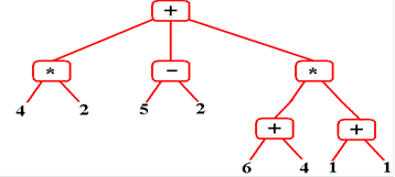
Evaluate
the prefix expression: ( + ( * 4
2 ) ( – 5 2 ) ( * ( + 6 4) (+ 1 1 ) ) )
(*
4 2) can be evaluated, so: (
+ 8 ( – 5 2 ) ( * ( + 6 4) (+ 1 1 ) ) )
(–
5 2) is defined as 5 – 2, so: (
+ 8 3 ( * ( + 6 4) (+ 1 1 ) ) )
(+
6 4) can be evaluated, so: (
+ 8 3 ( * 10 (+ 1 1 ) ) )
(+
1 1) can be evaluated, so: (
+ 8 3 ( * 10 2 ) )
(*
10 2) can be evaluated, so: (
+ 8 3 20 )
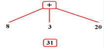
(+ 8 3 20) = 31,
so: 31
More on Postfix Evaluation
Consider again
the postfix expression YZ·X+. How is this evaluated? Any efficient evaluation
must use a data structure called a stack. Stacks
are LIFO (Last In, First Out) data structures.
Stacks are the data structure most naturally fit to evaluate expressions in
postfix notation. The
stack is best viewed as an abstract data type with specific methods, each of
which has a well
defined semantic (we can say exactly what it does).
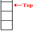 We can also consider the stack as having a top. Items are added to
the stack top and then removed from the stack top. The position of the
stack top is indicated by a stack pointer (SP).The stack data type has
three necessary methods, and two optional methods. The mandatory
methods are Push, Pop, and IsEmpty. The standard optional methods
are Top, and IsFull.
Note: When studying
computer networks, we speak of a “protocol stack”, which has
nothing to do with the ADT
(Abstract Data Type) stack that we study today.
We shall discuss the TCP/IP
protocol stack later in this course.
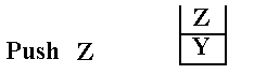
Pushing Items onto the Stack
Consider the sequence: Push (X),
Push (Y), and Push (Z). This sequence
adds three items to
the stack, in the specified order.
![]() Push X
Push X
Push Y
Push Z
After the third operation, Z is at the top of the stack and is
the first to be removed when a Pop
operation is performed. The SP (Stack
Pointer) is a data item internal to the stack that indicates
the location of the top of the stack. It
is never made public by any proper stack implementation.
We now consider the use of a stack to evaluate the postfix
expression YZ·X+.
Such an
expression is also called RPN for Reverse Polish Notation.
Rules: 1. Scan left to right.
2. Upon reading a variable, push it onto the stack.
3. Upon reading a dyadic operator, pop two variables from the
stack,
perform the operation, and push the result.
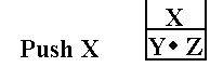
We read the first character and find it to be a variable: Y
![]()
We read the next character and find it also to be a
variable: Y Z
We read the next character and find
it to be an operator: Y Z ·
.
This is a dyadic operator (taking two arguments), so the stack is popped twice
to get the
two, the product is evaluated, and pushed back onto the stack.
![]()
We read the next character and find it to be a variable: Y Z · X
We read the last character and find
it to be an operator: Y Z · X +
Again, this is a dyadic operator, so two arguments are popped from the stack,
added, and
the sum pushed back onto the stack.
![]()
After this, the stack will be popped and the value placed
into some variable. This example
just looked at the expression, without considering the assignment.
Some of the early handheld calculators manufactured by
Hewlett–Packard, such as the HP–35,
used RPN (Reverse Polish Notation). To
add two numbers, say 20 and 35, do the following:
1. Punch the keys for 20 and then hit enter.
2. Punch
the keys for 35 and then hit enter.
3. Punch
the “+” key to add the two numbers.
4. The
number 55 is displayed.
More
on Prefix Evaluation
While a postfix
expression is evaluated using a stack, a prefix expression is evaluated using
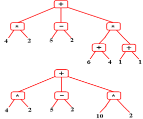
an expression tree. The expression is (
+ ( * 4 2 ) ( – 5 2 ) ( * ( + 6 4) (+ 1 1 ) ) ). Here is the
expression tree constructed for this expression.
Software to
evaluate this prefix expression would first build this tree (not very hard to
do) and
then evaluate it. For example, the node
(+ 6 4) would be replaced by 10, etc.
The expression
tree is evaluated by successively finding the leaf nodes, applying the
operation
in the parent node, and replacing that parent node with a leaf node with the
correct value.
The final value
of this expression is found when the tree collapses to a root node. It is 31.
Almost all
high–level languages, such as FORTRAN, COBOL, C/C++, and Java support
expressions in infix form only. LISP is
the only language known to this author that used the
prefix form. The language FORTH, and
some others, use postfix form.
What we have
been discussing to this point is the structure of expressions in a high–level
language. This is the result of a design
choice made by the language developers.
We now
turn to similar issues in the ISA, which are the result of the hardware design
of the CPU.
Structure of the Machine Language
We now consider
ISA (Instruction Set Architecture) implications for the evaluation of common
expressions. This is the sort of issue
seen in the HP–35, mentioned above. It
is not that one
might want to enter RPN into this calculator; RPN expressions are the only type
that the device
can evaluate. An attempt to enter
something like “20 + 30 =” would be an error.
We now consider
some pseudo–assembly language translations of a simple assignment
statement, specifically C = A + B. The
expression “A + B” is evaluated and the result is
stored in the memory location associated with the variable C.
Stack architecture
In this all operands are found on a stack.
These have good code density (make good use
of memory), but have problems with access.
Typical instructions would include:
Push X // Push the value
at address X onto the top of stack
Pop Y // Pop the top
of stack into address Y
Add // Pop the top
two values, add them, & push the result
Here
is an approximate assembly language translation of C = A + B
Push A
Push B
Add
Pop C
This stack
architecture is sometimes called “zero argument” as the mathematical operators
do not take explicit arguments. Only the
push and pop operators reference memory.
Single Accumulator Architectures
There is a
single register used to accumulate results of arithmetic operations. Many hand held
calculators with a single display line for the result are good examples of
this. The display
shows the result of one register, which could be called an accumulator.
The
single–accumulator realization of the instruction C = A + B
Load A //
Load the AC from address A
Add B //
Add the value at address B
Store C //
Store the result into address C
In each of these
instructions, the accumulator is implicitly one of the operands and need not be
specified in the instruction. This saves
space. The single accumulator can be
used to hold the
results of addition, subtraction, logical bit–wise operators, and all types of
shifts.
The single
accumulator cannot handle multiplication and division, except in restricted
cases.
The reason is that the product of two 16–bit signed numbers will be a 32–bit
signed product.
Consider squaring 24576 (214 + 213) or 0110 0000 0000
0000 in 16–bit binary. The result is
603, 979, 776 or 0010 0100 0000 0000 0000 0000 0000 0000.
We need two
16–bit registers to hold the result. The
PDP–9 had the MQ and AC. On the
PDP–9, the results of this multiplication would be
MQ 0010 0100 0000 0000 // High 16 bits
AC 0000 0000 0000 0000 // Low 16 bits
General Purpose Register Architectures
These have a
number of general purpose registers, normally identified by number. The number
of registers is often a power of 2: 8, 16, or 32 being common. (The Intel architecture with its
four general purpose registers is different.
These are called EAX, EBX, ECX, and EDX – a lot
of history here). Again, we shall
discuss these registers in the next two sub–chapters.
The names of the
registers often follow an assembly language notation designed to differentiate
register names from variable names. An
architecture with eight general purpose registers might
name them: %R0, %R1, …., %R7. The prefix
“%” here indicates to the assembler that we are
referring to a register, not to a variable that has a name such as R0. The latter name would be
poor coding practice.
Designers might
choose to have register %R0 identically set to 0. Having this constant register
considerably simplifies a number of circuits in the CPU control unit. We shall return to this
%R0 º 0 when
discussing addressing modes.
Note that a
general–purpose register machine can support memory–to–memory operations,
without direct use of any general–purpose registers. One example is a three argument version
of the VAX–11 add operation, ADDL3 A, B, C, which takes
the contents of address B, adds
the contents of address C, and stores the result in address A. Another typical example is the
packed decimal add instruction from the IBM S/360: AP S1,S2 // Add packed S2 to S1,
which adds the packed decimal value at address S2 to that at address S1.
General Purpose Registers with Load–Store
A Load–Store architecture is one with a
number of general purpose registers in which the only
memory references are: 1) Loading a register from memory, and 2) Storing a
register to memory
The realization
of our programming statement C = A + B might be something like
Load %R1, A // Load memory location A
contents into register 1
Load %R2, B //
Load register 2 from memory location B
Add %R3, %R1, %R2 // Add
contents of registers %R1 and %R2,
//
placing the result into register %R3
Store %R3, C //
Store register 3 into memory location C
It has been
found that the load–store design philosophy yields a simpler control unit,
especially
when dealing with virtual memory. The
problem standard designs have is the occurrence of a
page fault in the middle of instruction execution. We shall discuss page faults when we discuss
virtual memory in a later chapter.
It
is worth note that the standard general–purpose register machines, such as the
VAX–11/780 or
the IBM S/360, can easily be programmed in the style of a load–store machine,
though neither
is a load store machine. Here is a
fragment of S/360 assembly language written in the
load–store format.
L 5,A
// Load register 5 from location A
L
6,B // Load register 6 from
location B
AR 6,5 // Add contents of register 5 to register
6
ST 6,C // Store register 6 into location C
A note on the
comments. In IBM assembly language, the
comment begins with the first space
following the arguments. Here the “//”
are just from habit; they are not significant.
Modern Design Principles and RISC
The RISC (Reduced Instruction Set
Computer) movement advocated
a simpler design with
fewer options for the instructions.
Simpler instructions could execute faster. Machines that
were not RISC were called CISC (Complex
Instruction Set Computers).
One of the main
motivations for the RISC movement is the fact that computer memory is no
longer a very expensive commodity. In
fact, it is a “commodity”; that is, a commercial item
that is readily and cheaply available.
Another motivation is the complexity of the control unit
on the CPU; a more complex instruction set makes for a more complex control
unit. This
control unit has to be designed to handle the slowest instruction, so that many
simpler and
faster instructions take longer than necessary to execute. If we have fewer and simpler
instructions, we can speed up the computer’s speed significantly. True, each instruction might
do less, but they are all faster.
The Load–Store
Design
One of the slowest operations is the access of memory, either to read values
from it or write
values to it. A load–store design restricts memory access to two instructions: load
register from
memory and store register to memory. A
moment’s reflection will show that this works only
if we have more than one register, possibly 8, 16, or 32 registers.
Modern Design Principles: Basic
Assumptions
Some assumptions
that drive current design practice include:
1. The
fact that most programs are written in high–level compiled languages. Provision of
a large general purpose
register set greatly facilitates compiler design. Consider the
following assembly language
translation of Z = (A*B) + (C*D).
Single
accumulator Multiple register
LOAD A L
4,A // With a single
accumulator,
MUL B
M 4,B // it is necessary to write
STORE T // the intermediate result
to
LOAD C L
6,C // temporary memory.
MUL D M
6,D // This extra memory access
ADD T AR
4,6 // takes time.
STORE Z ST
4,Z
2. The
fact that current CPU clock cycle times (0.25 – 0.50 nanoseconds) are much
faster
than
memory access times. Reducing memory
access will allow the program to execute
more nearly at the full CPU
speed.
3. The
fact that a simpler instruction set implies a smaller control unit, thus
freeing chip area
for
more registers and on–chip cache. It is
a fact that the highest pay–off design decision
is to place more cache memory
on the CPU chip. No other design decision
will give such
a boost to performance, except
the equivalent addition of general–purpose registers.
4. The
fact that execution is more efficient when a two level cache system is
implemented
on–chip. We have a split L1 cache (with an I–Cache for
instructions and a D–Cache for
data)
and a L2 cache. A split L1 cache allows
the CPU to fetch an instruction and access
data at the same time. In chapter 12, we shall argue that a two
level cache is much faster
than a single level cache of
the same total size.
5. The
fact that memory is so cheap that it is a commodity item.
Modern Design
Principles
1. Allow only fixed–length operands. This may waste memory, but modern
designs have plenty of it, and it is
cheap.
2. Minimize the number of instruction formats
and make them simpler, so that
the instructions are more easily and
quickly decoded.
3. Provide plenty of registers and the largest
possible on–chip cache memory.
4. Minimize the number of instructions that
reference memory. Preferred
practice is called “Load/Store” in
which the only operations to reference
primary memory are register loads
from memory and register stores into memory.
5. Use pipelined and superscalar approaches that
attempt to keep each unit
in the CPU busy all the time. At the very least provide for fetching one
instruction while the previous
instruction is being executed.
6. Push the complexity onto the compiler. This is called moving the DSI
(Dynamic–Static interface). Let Compilation (static phase) handle any
any issue that it can, so that
Execution (dynamic phase) is simplified.
RISC
(Reduced Instruction Set Computers)
One
of the recent developments in computer architecture is called by the acronym
RISC.
Under this classification, a design is either RISC or CISC, with the following
definitions.
RISC Reduced
Instruction Set Computer
CISC Complex
Instruction Set Computer.
The
definition of CISC architecture is very simple – it is any design that does not
implement
RISC architecture. We now define RISC
architecture and give some history of its evolution.
The
source for these notes is the book Computer Systems Design and Architecture,
by
Vincent P. Heuring and Harry F. Jordan [R011].
One
should note that while the name “RISC” is of fairly recent origin (dating to
the late 1970’s)
the concept can be traced to the work of Seymour Cray, then of Control Data
Corporation, on
the CDC–6600 and related machines. Mr.
Cray did not think in terms of a reduced instruction
set, but in terms of a very fast computer with a well-defined purpose – to
solve complex
mathematical simulations. The resulting
design supported only two basic data types (integers
and real numbers) and had a very simple, but powerful, instruction set. Looking back at the
design of this computer, we see that the CDC–6600 could have been called a RISC
design.
As
we shall see just below, the entire RISC vs. CISC evolution is driven by the
desire to obtain
maximum performance from a computer at a reasonable price. Mr. Cray’s machines maximized
performance by limiting the domain of the problems they would solve.
The
general characteristic of a CISC architecture is the emphasis on doing more
with each
instruction. This may involve complex
instructions and complex addressing modes; for example
the MC68020 processor supports 25 addressing modes.
The
ability to do more with each instruction allows more operations to be
compressed into the
same program size, something very desirable if memory costs are high.
Another
justification for the CISC architectures was the “semantic gap”, the difference
between
the structure of the assembly language and the structure of the high level
languages (COBOL,
C++, Visual Basic, FORTRAN, etc.) that we want the computer to support. It was expected that
a more complicated instruction set (more complicated assembly language) would
more closely
resemble the high level language to be supported and thus facilitate the
creation of a compiler for
the assembly language.
One
of the first motivations for the RISC architecture came from a careful study of
the
implications of the semantic gap.
Experimental studies conducted in 1971 by Donald Knuth and
1982 by David Patterson showed that nearly 85% of a programs statements were
simple
assignment, conditional, or procedure calls.
None of these required a complicated instruction
set. It was further notes that typical
compilers translated complex high level language constructs
into simpler assembly language statements, not the complicated assembly
language instructions
that seemed more likely to be used.
The
results of this study are quoted from an IEEE Tutorial on RISC architecture
[R05]. This
table shows the percentages of program statements that fall into five broad
classifications.
|
Language |
Pascal |
FORTRAN |
Pascal |
C |
SAL |
|
Workload |
Scientific |
Student |
System |
System |
System |
|
Assignment |
74 |
67 |
45 |
38 |
42 |
|
|
4 |
3 |
5 |
3 |
4 |
|
Call |
1 |
3 |
15 |
12 |
12 |
|
If |
20 |
11 |
29 |
43 |
36 |
|
GOTO |
2 |
9 |
-- |
3 |
-- |
|
Other |
|
7 |
6 |
1 |
6 |
The authors of
this study made the following comments on the results.
“There is quite
good agreement in the results of this mixture of languages and
applications. Assignment statements
predominate, suggesting that the simple
movement of data is of high importance.
There is also a preponderance of
conditional statements (If,
language with some sort of compare and branch instruction. This suggests that
the sequence control mechanism is important.”
The
“bottom line” for the above results can be summarized as follows.
1) As
time progresses, more and more programs will be written in a compiled high-
level language, with much
fewer written directly in assembly language.
2) The
compilers for these languages do not make use of the complex instruction
sets provided by the
architecture in an attempt to close the semantic gap.
In
1979, the author of these notes attended a lecture by a senior design engineer
from IBM. He
was discussing a feature of an architecture that he designed: he had put about
6 months of highly
skilled labor into implementing a particular assembly language instruction and
then found that it
was used less than 1/10,000 of a percent of the time by any compiler.
So
the “semantic gap” – the desire to provide a robust architecture for support of
high-level
language programming turned out to lead to a waste of time and resources. Were there any
other justifications for the CISC design philosophy?
The
RISC/370
This is your authors name for a
hardware / software architecture developed by David A.
Patterson [R010]. This experiment focused on the IBM S/360 and
S/370 as targets for a
RISC compiler. One model of interest was
the S/360 model 44. The S/360 model 44
implements only a subset of the
S/360 architecture in hardware; the rest of the functions are
implemented in software. This allows for a simpler and cheaper control
unit. The Model 44
was marketed as a low–end S/360,
less powerful and less costly.
A compiler created for the RISC computer IBM 801 was adapted
to emit code for the S/370
treated as a register–to–register
machine, in the style of a RISC computer.
Only a subset of the
S/370 instructions was used as a
target for the compiler. Specifically,
the type RX (memory and
register) arithmetic instructions
were omitted, as were the packed decimal instructions, all of
which are designed to be memory to
memory with no explicit register use.
This subset ran programs 50 percent faster than the previous
best optimizing compiler that used
the full S/370 instruction set. Possibly the S/370 was an overly complex
design.