The Motherboard
While the early
integrated circuits represented a significant advance in computer design, it
was
not until the introduction of VLSI (Very Large Scale Integrated) circuits that a significant
step
was made. By definition, a VLSI circuit
chip contains at least 100,000 transistors, corresponding
to about 30,000 to 50,000 digital circuit elements. At this level of complexity, most of the
interconnections could be placed on the chips, leaving a rather modest number
of connections
required among the chips. Even then,
these connections were no longer implemented as wires,
but as traces etched onto a large circuit board, called the motherboard.
Here is a picture
of the motherboard of modern computers.
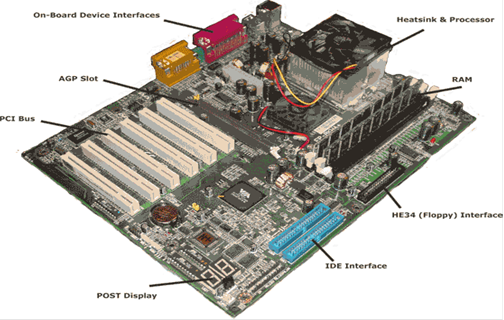
At this
resolution, the reader might be able to see the aluminum traces used to connect
the
insertion slots into which the components are placed. These traces greatly simplified the
manufacture of a motherboard by removing the necessity of a tangle of wiring,
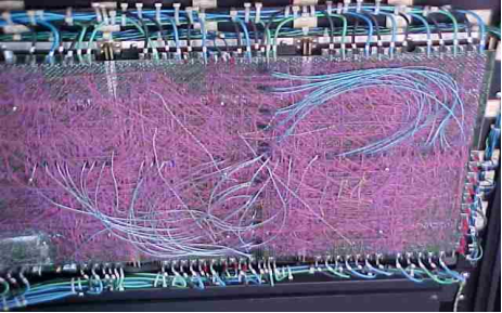
as seen in the
picture of the PDP–10 backplane. Note
the RAM at the upper right. There seem
to be two
memory modules, each a DIMM (Dual In–line Memory Module) with parity memory.
We shall discuss
the structure of modern memory in chapter 8.
As we have mentioned the term
“parity memory” here, we might as well explain a bit before moving on. A typical modern
memory module will be byte oriented, while the individual chips in the module
will be bit
oriented. One would expect to see a
memory module comprising eight memory chips, one for
each of the bits in an 8–bit byte. Close
inspection of the memory modules above shows that each
has nine chips, thus storing nine bits for each byte. The extra bit is a parity bit, used for error
detection. Consider the entry PD7D6D5D4D3D2D1D0
. The eight bits, D7D6D5D4D3D2D1D0,
store
the byte. The value of the parity bit,
P, is determined by the parity convention used.
The
number of 1 bits in the byte are counted; the byte 0101 0111 would have
five. In even parity
memory, the requirement is that the nine bits stored have an even count of 1
bits; the above byte
(the ASCII code for “W”) would be stored as 1 0101 0111. In odd parity, the above byte
would be stored as 0 0101 0111. This is a simple error detection scheme.
We have already
mentioned Moore’s Law. Another
consequence of the progress predicted by
this law is the increase in the amount of memory that can be placed on a single
DIMM. This
increase is driving new connection techniques with increased pin count. As a consequence, one
cannot confidently say how many pins are to be found on a DIMM without knowing
the year of
its manufacture. The following picture
shows both sides of a reasonably modern DIMM.
A quick count shows eight memory chips on the module; this is non–parity
memory.
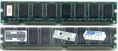
Note the pins at
the bottom of the DIMM. These pins are
inserted into a slot (socket) on the
motherboard. A quick count of the pins
shows the number to be “quite a few”.
The next picture
shows an enlargement of the area of the motherboard with the DIMM slots.
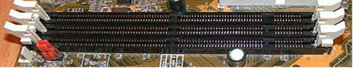
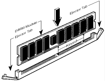
The final figure
of this sequence on memory shows how the DIMM are inserted. The DIMM in
this figure does support parity memory.
The smaller chip is a memory controller on the DIMM.
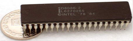
The manner of
attachment of the CPU to the motherboard requires some discussion. Early CPU
chips, such as the Intel 8086, were connected as simple Dual In–Line chips. This chip has forty
pins, twenty in a row on each side.
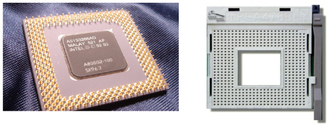
As the
complexity of the Central Processing Unit grew, the number of pins to connect
it to the
motherboard grew. Fairly soon, the
dual–in–line approach was no longer sufficient and the
design had to move to a square array of pins on the bottom of the chip. The following picture
shows an early model Pentium with a later model socket. These figures just illustrate the
concept; the CPU chip will not fit into this socket.
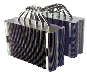
In order to cool
the CPU, the design calls for a heatsink, which can be viewed as a radiator
with
an electric fan to move air through it.
Some enthusiasts, called “overclockers”, try to run the
CPU at a clock speed faster than is specified.
In these situations, a large heatsink is required.
The following picture shows a typical large commercial heatsink. The CPU is mounted on the
small square area at the top with the tubes protruding from it.
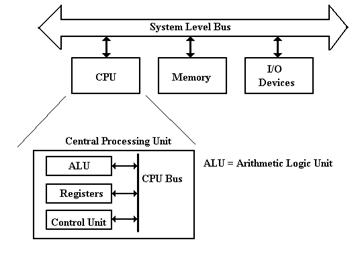
Components of a Modern Computer
The
four major components of a modern stored program computer are:
1. The
Primary Memory (also called “core memory” or “main memory”)
2. The
Input / Output system
3. The
Central Processing Unit (CPU)
4. One
or more system busses to allow the components to communicate.
Note that some authors do not
consider the bus when counting subsystems.
The system memory (of which your author’s computer has 512 MB) is used
for transient
storage of programs and data. This is
accessed much like an array, with the memory
address serving the function of an
array index. Later chapters in this book
will consider the
structure of this memory, including the use and advantages of cache memory.
The Input / Output system (I/O System) is used for the computer to save
data and programs
and for it to accept input data and communicate output data. The keyboard is an input device,
the video display is an output device. Technically
the hard drive is an I/O device,
though we
can also consider it as a part of the memory system. As we shall see, I/O devices are divided
into classes by speed of data transfer, with controlling hardware adapted to
the speed.
The Central Processing Unit (CPU) handles execution of the program.
It has four main components:
1. The
ALU (Arithmetic Logic Unit), which
performs all of the arithmetic
and logical operations of
the CPU, including logic tests for branching.
2. The
Control Unit, which causes the CPU
to follow the instructions
found in the assembly
language program being executed.
3. The
register file, which stores data internally in the CPU. There are user
registers and special
purpose registers used by the Control Unit.
4. A
set of 3 internal busses to allow the CPU units to communicate.
A System Level Bus, which allows the top–level components to
communicate. The idea of
a single system bus is logically correct, and has been implemented on many
early designs
including the PDP–11, of which your author is so fond.
This design was
acceptable for older computers, but is not acceptable for modern designs.
Basically,
a single system level bus cannot handle the data load expected of modern
machines.
Modern gamers
demand fast video; this requires a fast bus to the video chip. The memory
system
is always a performance bottleneck. We
need a dedicated memory bus in order to allow
acceptable
performance. Here is a refinement of the
above diagram.
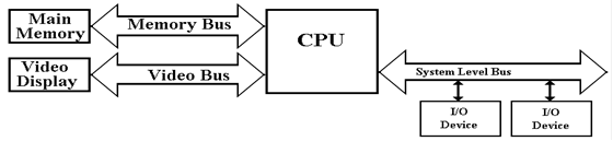
This design is
getting closer to reality. At least, it
acknowledges two of the devices requiring
high
data rates in access to the CPU. We now turn to commercial realities, specifically legacy
I/O devices. When
upgrading a computer, most users do not want to buy all new I/O devices
(expensive) to replace older devices that still function well. The
I/O system must provide a
number of busses of different speeds, addressing capabilities, and data widths,
to
accommodate this variety of I/O devices.
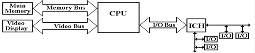
Here we show the main I/O bus
connecting the CPU to the I/O Control
Hub (ICH), which is
connected to two I/O busses: one for slower (older) devices, one for faster
(newer) devices.
Note that each
of the revised designs has two, or possibly three, point–to–point busses. The
memory
bus is a good example of a point–to–point bus; it connects only two
devices. The end
result
is a significant improvement in data transfer speed, something that is demanded
of this
bus. The downside is the complexity of the design.
While it would
offer significant speed advantages for each component to be connected directly
to
all
of the other components, this option was not taken due mostly to the design
complexity. Any
scheme
connecting N devices via point–to–point busses must have N·(N – 1) /2 busses. This
would
be 120 data busses for just 16 devices.
The number grows quadratically.
Just because the
author likes to show off, he presents a
proof
of this coun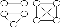 t, using basic
induction. Two devices have 1
connection, 3
t, using basic
induction. Two devices have 1
connection, 3
devices
have 2 connections, and four devices have 6.
If
N devices have N·(N – 1) /2
connections, and we
add
another device, we must connect the new device
to
the original N devices.
The new total is
N·(N – 1) /2 + N = [N·(N
– 1) + 2N] / 2 = [N2 – N + 2N] / 2
=
[N2 + N] / 2 = N·(N + 1) /2.
The modern
computer will have a bus structure suggested by the second modification. The
requirement to handle memory as well as a proliferation of I/O devices has lead
to a new
design based on two controller hubs:
1. The Memory Controller Hub or “North
Bridge”
2. The I/O Controller Hub or “South
Bridge”
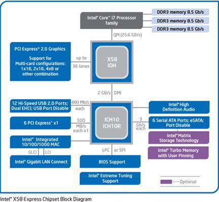
Such a
design allows for grouping the higher–data–rate connections on the faster
controller,
which is closer to the CPU, and grouping the slower data connections on the
slower controller,
which is more removed from the CPU. The
names “Northbridge” and “Southbridge” come from
analogy to the way a map is presented.
In almost all chipset descriptions, the Northbridge is
shown above the Southbridge. In almost
all maps, north is “up”. It is worth
note that, in later
designs, much of the functionality of the Northbridge has been moved to the CPU
chip.
The System Clock
The modern computer is properly
characterized as a synchronous sequential circuit. For the
purposes of this course, a sequential
circuit is one that has memory. The ALU (Arithmetic
Logic Unit) is not a sequential circuit as its output depends only on the
input at the time. It does
not store results or base its computations on any previous inputs. The most fundamental
characteristic of synchronous circuits is
a system clock, used to coordinate processing.
This is
an electronic circuit that produces a repetitive train of logic 1 and logic 0
at a regular rate, called
the clock frequency. Most computer systems have a number of
clocks, usually operating at
related frequencies; for example – 2 GHz, 1GHz, 500MHz, and 125MHz.
The inverse of the clock frequency
is the clock cycle time or period.
As an example, we
consider a clock with a frequency of 2 GHz (2·109 Hertz).
The cycle time is 1.0 / (2·109)
seconds, or 0.5·10–9
seconds = 0.500 nanoseconds = 500 picoseconds.
A slower bus clock
with a frequency of 250 MHz (2.5·108 Hertz) would have a period of 1.0 / (2.5·108) seconds,
or 4.0·10–9 seconds = 4.0
nanoseconds.
Synchronous sequential circuits are sequential circuits that use a clock input to
order events.
Asynchronous sequential circuits do not use a common clock and are much harder
to design and
test. As we shall focus only on
synchronous circuits, we immediately launch a discussion of the
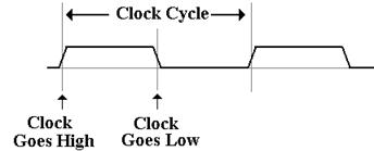
clock. The following figure illustrates
some of the terms commonly used for a clock.
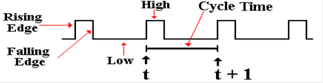
The clock input is very important to the concept of a
sequential circuit. At each “tick” of
the
clock the output of a sequential circuit is determined by its input and by its
state. We now
provide a common definition of a “clock tick” – it occurs at the rising
edge of each pulse. In
synchronous circuits, this clock tick is used to coordinate processing events.
Diversion: What the Clock Signals
Really Look Like
The figure above represents the clock as a well-behaved
square wave. This is far from the actual
truth, as can be seen by examining the clock pulses with sufficient
resolution. The following
figure presents three views of the clock pulse train produced by a typical
clock: a realistic
physical view and two notations for approximating the clock. In reality, the clock pulse is not
square, but rises and falls exponentially.
This is shown in the top view.
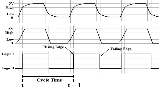
For those with mathematical interest, the clock falls in a
function of the form e –ax and rises
with
the form of the function 1 – e –bx, where a »
b.
Use of this precise form does not gain us
anything and leads to significant difficulties, so that unless we are
troubleshooting at a very low
level, we approximate the clock by either a trapezoidal wave or a square wave.
The trapezoidal wave form is used
when it is important to emphasize the fact that the clock does
take some time to rise and fall. One
sees this form of clock representation often when examining
timing diagrams for system buses. The
square wave is a further abstraction of the real electrical
form of the wave; fortunately it is quite often an adequate
representation. The square wave
representation remains at logic 0 until the real electrical clock crosses the
threshold for logic high
at which time the square wave jumps to logic 1.
The square wave remains at logic 1 until the
real electrical clock signal crosses the threshold for logic low at which time the square wave
goes to logic 0. The figure above is
drawn to reflect that fact.
In any system of electronics based
on positive voltages, there are three voltage ranges. There is a
threshold voltage below which the signal is interpreted as a logic 0. There is another threshold
voltage above which the signal is interpreted as a logic 1. There is also a “middle level” in
which the device is not required to assign a consistent logic value. The original values were
specified by Texas Instruments for its TTL
(Transistor–Transistor Logic, most
gates had two
transistors) circuits. The standard is
based on a full voltage of 5.0 volts.
2.8
to 5.0 volts logic 1
0.8 to 2.8 volts indeterminate, may be interpreted as
either logic 0 or logic 1
0.0 to 0.8 volts logic 0.
Earlier we hinted at the heat
problem in a CPU and discussed the problems associated with
cooling it to a temperature at which it would operate reliably. One law of physics is that the heat
emitted by a circuit varies as the square of the power supplied to it. For this reasons, modern
computer designs have reduced the operating voltage, first to 3.5 volts and
then to 1.8 volts.
Consider (5.0/1.8)2 = 7.72. A
5 volt CPU produces over seven times the heat of a 1.8 volt unit.
With some minor reworking of the circuitry, the CPU would perform just as well
at the lower
voltage. Given the recent emphasis on
power management, the voltage change was adopted.
As noted above,
if a bus has a clock it is usually slower than the system clock. This is achieved
by
use of a straightforward sequential circuit called “divide by N”. For example, a
system clock
signal
at 2.0 GHz might be input into a “divide by 4” circuit to output a signal at 500
MHz.
Computer
Busses
We now turn our attention to computer busses. A bus is nothing more than a collection of
wires
(or etched signal traces) along which a set of related electrical signals is
sent. Busses are often
characterized by their “width”, which is the number of signal wires the bus
contains.
Signals
that traverse a bus can be divided into three groups:
1. Data – usually 32 bits or 64 bits at a
time.
2. Address – now commonly either 32 bits or 64 bits.
3. Control – a number of lines for controlling the
bus activities.
A bus may be either multiplexed or non–multiplexed. In a multiplexed
bus, bus data and
address share the same lines, with a control signal to distinguish the
use. A non–multiplexed
bus has separate lines for address and data.
The multiplexed bus is cheaper to build in that it
has fewer signal lines. A
non–multiplexed bus is likely faster.
There is a variant of multiplexing, possibly called “address multiplexing” that is seen on
most
modern memory busses. In this approach,
an N–bit address is split into two (N/2)–bit addresses,
one a row address and one a column address.
The addresses are sent separately over a dedicated
address bus, with the control signals specifying which address is being
sent. Modern memory
chips are designed to be addressed in two stages, called row address and column
address.
Another way to characterize busses is whether the bus is
asynchronous or synchronous. A
synchronous bus is one that has one
or more clock signals associated with it, and transmitted
on dedicated clock lines. In a
synchronous bus, the signal assertions and data transfers are
coordinated with the clock signal, and can be said to occur at predictable
times. Synchronous
busses require all attached devices to operate at fixed speeds, either the bus
clock speed or some
integer fraction of that speed; a 400 MHz bus might have devices at 400 MHz,
200 MHz, or
100 MHz. Such a bus is easier to design
than an asynchronous bus.
An asynchronous
bus is one without a clock signal. The
data transfers and some control signal
assertions on such a bus are controlled by other control signals. Such a bus might be used to
connect an I/O unit with unpredictable timing to the CPU. The I/O unit might assert some sort of
ready signal when it can undertake a
transfer and a done signal when the
transfer is complete.
The memory bus used to be asynchronous, but modern memory is synchronous. Think of main
memory advertised as being “133 MHz”.
This is the frequency of the memory bus.
Bus Signal Levels
Many times bus operation is illustrated with a timing diagram
that shows the value of the digital
signals as a function of time. Each
signal has only two values, corresponding to logic 0 and to
logic 1. The actual voltages used for
these signals will vary depending on the technology used.
A bus signal is
represented in some sort of trapezoidal form with rising edges and falling
edges,
neither
of which is represented as a vertical line.
This convention emphasizes that the signal
cannot
change instantaneously, but takes some time to move between logic high and
low. Here
is
a depiction of the bus clock, represented as a trapezoidal wave.
As noted above,
this trapezoidal wave form is used in bus timing diagrams just to remind the
reader
that the signal transitions are not instantaneous. Square waves would work just as well.
Signal
Assertion Levels
A control signal
is said to be asserted when it
enables some sort of action. This
applies to any
component
of the computer, but here we are discussing bus transfers. Some signals are asserted
by
being driven to a logic 1 (5.0 volts for TTL), but most are asserted by being
driven to logic 0
(any
voltage less than 0.8 volts for TTL, but commonly 0 volts). There are several notations
used
to denote these signals. The book by Rob
Williams uses an older notation. We use
both.
Here
are the notations used for active low
signals, that is signals that are asserted at logic 0.

The over–bar is
less used now, as it is not common for word processors to have this format
feature. A two–value signal is one that has meaning
for each of its values. One of the
easiest to
understand
is  ;
when 1 the first option is asserted, when 0, the second option is asserted.
;
when 1 the first option is asserted, when 0, the second option is asserted.
The standards
for denoting these signals are illustrated by the controls for a standard RAM
(Random Access Memory),
discussed in detail below. We need two control signals to
specify the three options for a RAM unit.
One standard set is
 – the memory
unit is selected. This signal is active
low.
– the memory
unit is selected. This signal is active
low.
– if 0 the CPU
writes to memory, if 1 the CPU reads from memory.
We can use a truth table to specify
the actions for a RAM. Note that when = 1,
|
|

|
Action
|
|
1
|
0
|
Memory
contents are not changed.
|
|
1
|
1
|
Memory
contents are not changed.
|
|
0
|
0
|
CPU
writes data to the memory.
|
|
0
|
1
|
CPU
reads data from the memory.
|
nothing is happening to the
memory.
It is not being accessed by the CPU
and the contents do not change. When
= 0, the memory
is active and
something happens.
Recent there has
been a change in the notation to denote the asserted low signals, replacing the
over–bar
by a sharp sign. Given this convention,
the table above would have been show as:
|
Select#
|
R/W#
|
Action
|
|
1
|
0
|
Memory
contents are not changed
or accessed. Nothing happens.
|
|
1
|
1
|
|
0
|
0
|
CPU
writes data to the memory.
|
|
0
|
1
|
CPU
reads data from the memory.
|
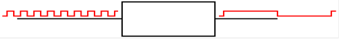
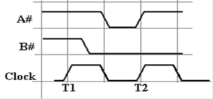
Here is a sample diagram, showing two hypothetical
discrete signals. Here the discrete
signal B#
goes
low during the high phase of clock T1 and stays low. Signal A# goes low along with the
second
half of clock T1 and stays low for one half clock period.
A collection of
signals, such as 32 address lines or 16 data lines cannot be represented with
such
a
simple diagram. For each of address and
data, we have two important states; the signals are
valid,
and signals are not valid
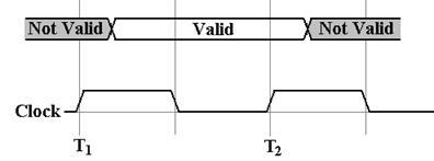
For example,
consider the address lines on the bus.
Imagine a 32–bit address. At some
time
after
T1, the CPU asserts an address on the address lines. This means that each of the 32 address
lines
is given a value, and the address is valid until the middle of the high part of
clock pulse T2,
at
which the CPU ceases assertion.
Having seen these conventions, it is time to study a pair of
typical timing diagrams. We first
study the timing diagram for a synchronous bus.
Here is a read timing diagram.
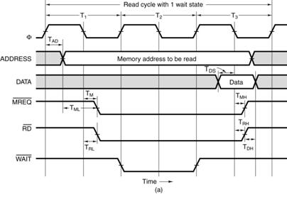
What we have here is a timing diagram that covers three full
clock cycles on the bus. Note that
during the high clock phase of T1, the address is asserted on the
bus and kept there until the low
clock phase of T3. Before and
after these times, the contents of the address bus are not specified.
Note that this diagram specifies some timing constraints. The first is TAD, the maximum
allowed
delay for asserting the address after the clock pulse if the memory is to be
read during the high
phase of the third clock pulse.
Note that the memory chip will assert the data for one half
clock pulse, beginning in the middle
of the high phase of T3. It
is during that time that the data are copied into the MBR.
Note that the three control signals of interest, now called MREQ#, RD#, and WAIT# are
asserted low. The reason for changing
from the over–bar notation is that your author’s word
processing program was consistently messing up the format when displaying that.
We also have another constraint TML, the minimum
time that the address is stable before the
signal MREQ#
is asserted. The purpose of the diagram
above is to indicate what has to happen
and when it has to happen in order for a memory read to be successful via this
synchronous bus.
We have four discrete signals (the clock and the three control signals) as well
as two multi–bit
values (memory address and data).
For the discrete signals, we are interested in the specific
value of each at any given time. For the
multi–bit values, such as the memory address, we are only interested in
characterizing the time
interval during which the values are validly asserted on the data lines.
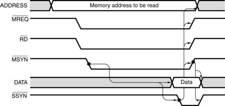
The timing diagram for an asynchronous bus includes some
additional information. Here the
focus is on the protocol by which the two devices interact. This is also called the “handshake”.
The bus master asserts MSYN# and the
bus slave responds with SSYN# when
done.
The asynchronous bus uses similar notation for both the
discrete control signals and the
multi–bit values, such as the address and data.
What is different here is the “causal arrows”,
indicating that the change in one signal is the causation of some other
event. Note that the
assertion of MSYN# causes the memory
chip to place data on the bus and assert SSYN#. That
assertion causes MSYN# to be
dropped, data to be no longer asserted, and then SSYN# to drop.
The
Fetch–Execute Cycle
As noted several times before in
this text, a stored program computer operates by fetching
instructions from memory and executing them; this is the “fetch–execute cycle”.
Depending on
the level of detail one wishes to discuss, there are quite a few ways to
characterize this process.
One common way is to break the cycle into three parts:
1. Fetch the instruction is copied from memory
into the CPU.
2. Decode the control logic identifies the
instruction.
3. Execute the CPU executes the instruction and
possibly writes the result to memory.
Your instructor has written a
textbook on Computer Architecture, in which he wants to focus on
addressing modes in a computer. For this
purpose, he breaks the cycle also into 3 parts: fetch,
defer, and execute. Others may break the
cycle into 5 phases, or as many as 12.
No matter how it is described, the
basic function of the fetch–execute cycle is the same: bring
instructions from the memory and execute them.
At the time an instruction is fetched from
memory, it has been converted to binary machine code and stored at a fixed
memory location.
In raw form, the binary instructions
are almost unreadable. Here is how the
code might appear in
a hexadecimal data representation, in which each hexadecimal digit represents
32 binary bits.
We shall first show a listing with eight hexadecimal digits per line and then
show the meaning of
the code. We shall not present the
absolute binary. Hexadecimal notation is
covered soon.
B8 23 01
05
25 00 8B D8
03 D8 8B CB
2B C8 2B C0
EB EE
The process of converting this mess
into something that can be understood is called disassembly.
We shall work with that in the near future.
The key is to find the opcode in the machine code
listing and then to identify what other digits go with it. In the first line, we would note that the
one–byte value B8 is the numeric code for moving a value into a register, an
instruction that is
three bytes in length. Hence the first
complete instruction is B82301. Here is the
complete
disassembly of the above code fragment.
It seems to be toy code with little real purpose.
B82301 MOV
AX, 0123 Move value 0x0123 to AX
052500 ADD AX, 0025 Add value 0x0025 to AX
8BD8 MOV BX, AX Copy contents of AX into BX
03D8 ADD BX, AX Add contents of BX to AX
8BCB MOV CX, AX Copy contents of AX into CX
2BC8 SUB CX, AX Subtract AX from CX
2BC0 SUB
AX, AX Subtract AX from AX,
clearing it
EBEE JMP 100 Go to address 100
The above mess shows the advantage
of using assembly language over pure binary code, and
further the significant advantage of coding in a higher level language.
At this point, we mention three
registers found in the Pentium CPU. As
noted above, both
registers and memory store data. The
primary difference between a register and a memory word
is that the register is considered logically a part of the CPU, while memory is
considered a
separate subsystem. Two of these
registers, IP and IR, are special purpose registers; they
are
used by the CPU Control Unit and cannot be referenced directly by the
program. The other
register, AX, is a general purpose
register; assembly language instructions can reference it
directly and often do. Here are the definitions
of these registers.
AX This
is also called the Accumulator, in
that it accumulates results. The best
analogy is the display on
a single line calculator, which holds the results of the
calculation as it
progresses. As we shall see later, there
are a number of ways to
access the accumulator;
as AX it is 16 bits, as EAX it is 32 bits.
IR This
is called the Instruction Register. The fetch–execute cycle functions by
copying a binary machine
language instruction into the Instruction Register for
access by the Control
Unit, which decodes it and begins execution.
IP This
is the Instruction Pointer, pointing
to the instruction to be fetched next.
Other designs call this
register the PC or Program Counter, probably because it
does not count
anything. As an efficiency, while one
instruction is executing the
Instruction Pointer is
already pointing to the next instruction.
This often causes
confusion for the
inexperienced assembly language programmer.
Using pseudo–Java, the instruction
fetch is simply described: IR
= Memory[IP++].
Instruction Prefetching
There have been a number of design
changes undertaken in order to speed up the execution of
machine language instructions. One is
based on the realization that the execution of one
instruction can be done in parallel with the fetching of the next
instruction. This design option,
called “prefetching” works because
instructions are normally executed in sequence.
Breaks in
the sequence, such as loops, jumps, and subroutine calls tend to be less
common.
Here is a diagram showing the idea
of a prefetch unit. The idea originated
with the IBM 7030,
called “Stretch” in the late 1950’s.
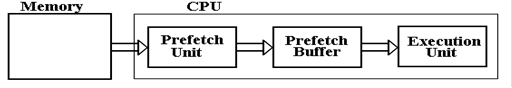
The prefetch buffer is implemented
in the CPU with on–chip registers. It is
implemented as a
single queue, which is a FIFO (first–in, first–out) data structure. Normally the instructions are
issued to the execution unit in the order they are fetched and placed in the
prefetch buffer.
When the execution of one instruction completes, the next one is already in the
buffer and can be
quickly executed. Any program branch
(loop structure, conditional branch, etc.) will invalidate
the contents of the prefetch buffer, which must be reloaded.
The
Memory Component
We shall speak of computer memory in
more detail in chapters 6 and 12 of this textbook. For the
moment, we shall confine ourselves to a few general remarks. The memory stores the
instructions and data for an executing program.
Memory is characterized by the smallest
addressable unit:
Byte
addressable the smallest unit is an 8–bit byte.
Word
addressable the smallest
unit is a word, usually 16 or 32 bits in length.
Most modern computers are byte addressable,
facilitating access to character data. The
CPU has
two registers dedicated to handling memory.
The
MAR (Memory Address Register) holds the
address being accessed.
The
MBR (Memory Buffer Register) holds the data
being written to the memory or being
read from the memory. This is sometimes called the Memory Data Register.
We have already discussed the memory
control signals issued by the CPU when we used them as
an example of notation for bus control.
Here they are again, Select# and
R/W#.
|
Select#
|
R/W#
|
Action
|
|
1
|
0
|
Memory
contents are not changed
or accessed. Nothing happens.
|
|
1
|
1
|
|
0
|
0
|
CPU
writes data to the memory.
|
|
0
|
1
|
CPU
reads data from the memory.
|
Byte
Addressing vs. Word Addressing
The addressing capacity of a
computer is dictated by the number of bits in the MAR. If the
MAR (Memory Address Register Contains) N bits, then 2N items can be
addressed. In a byte
addressable machine, the maximum memory size would be 2N bytes. If the machine is word
addressable, with 2–byte words, the maximum memory size is 2N words
or 2N+1 bytes.
Word addressable machines might have their memory sized
quoted in bytes, but they do not
access individual bytes. As an example,
we examine two obsolete computers, the PDP–11/70
and the CDC–6600. Each used an 18–bit
address; the PDP–11/70 addressed 256 KB, the
CDC–6600 addressed 256 K words (60 bits each).
The CDC–6600 could have been considered
to have 1,920 KB of memory. However, it
was not byte addressable; the smallest addressable
unit was a 60–bit integer.
Almost every modern computer is byte addressable to allow
direct access to the individual bytes
of a character string. A modern computer
that is byte addressable can still issue both word and
longword instructions. These just
reference data two bytes at a time and four bytes at a time.
Word
Addressing in a Byte Addressable Machine
Each 8–bit byte has a distinct
address. A 16–bit word at address Z
contains bytes at addresses Z
and Z + 1. A 32–bit word at address Z
contains bytes at addresses Z, Z + 1, Z + 2, and Z + 3.
Note that computer organization and architecture refer to addresses, rather
than variables.
The idea of a variable is an artifact of higher level languages.
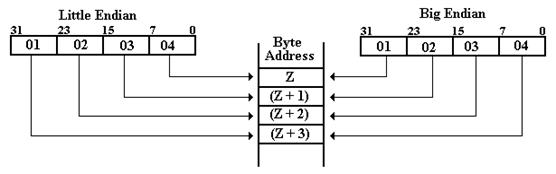
Big–Endian
vs. Little–Endian Addressing
Here is a problem. Consider a 32–bit integer, which takes four
bytes to store. Suppose that the
value is in the 32–bit accumulator, EAX. Following standard practice, we number the
bits in the
integer with values from 0 through 31.
Following practice that is standard for every computer
design except the IBM Mainframe series, we number the most significant bit 31
and the least
significant bit 0. We assume that the
hexadecimal value 0x01020304 is stored in this register.
For those who are interested, the decimal value is 16, 909, 060.

Suppose the instruction MOV Z, EAX is executed. What is placed into address Z. This depends
on whether the Pentium is a big–endian or little–endian device. (It is a big–endian device, but
we shall examine both options.)
Here is one representation of the two options for storing
the value. The value that goes into
each address is a one–byte number, comprising two hexadecimal digits.
Address Big-Endian Little-Endian
Z 01 04
Z + 1 02 03
Z + 2 03 02
Z
+ 3 04 01
The following diagram might make things more obvious. Note that the value in the
32–bit register EAX is the same on both sides.
Example:
“Core Dump” at Address 0x200
Basically a core dump is an obsolete term for a listing, by address, of the
hexadecimal values in
each addressable byte of primary memory.
The name is due to the fact that, for 20 to 30 years,
the most popular implementation of primary memory used magnetic cores. We have already
seen one example of a core dump in the above listing of binary machine code in
hexadecimal
format. Core dumps contain both
instructions and data; they are very tedious to read. It is here
that modern debugging tools really shine.
In reading these examples, remember the powers of
16, the basis of hexadecimal numbers.
The powers of 256 are 2560
= 1, 2561 = 256, 2562 = 65536, and 2563 =
16,777,216
Suppose one has the following memory map as a result of a
core dump. The memory is byte
addressable; each byte holds a number represented by two hexadecimal digits.
|
Address
|
0x200
|
0x201
|
0x202
|
0x203
|
|
Contents
|
02
|
04
|
06
|
08
|
What is the value of the 32–bit long integer stored at
address 0x200?
This is stored in the four bytes at addresses 0x200, 0x201,
0x202, and 0x203. For the
big–endian option, the number is 0x02040608.
Its decimal value is
2·2563 + 4·2562 + 6·2561 + 8·1 = 33,818,120
Little Endian: The
number is 0x08060402. Its decimal value
is
8·2563 + 6·2562 + 4·2561 + 2·1 = 134,611,970.
NOTE: Read the
bytes backwards, not the hexadecimal digits.
Example 2:
“Core Dump” at Address 0x200
Suppose one has the following memory
map as a result of a core dump.
The memory is byte addressable.
|
Address
|
0x200
|
0x201
|
0x202
|
0x203
|
|
Contents
|
02
|
04
|
06
|
08
|
What is the value of the 16–bit integer stored at address
0x200?
This number is stored in the two bytes at addresses 0x200
and 0x201. The bytes at addresses
0x202 and 0x203 are not part of this 16–bit integer.
Big Endian The
value is 0x0204.
The
decimal value is 2·256
+ 4 = 516
Little Endian: The
value is 0x0402.
The
decimal value s 4·256
+ 2 = 1,026
Simple
I/O – Parallel Ports
In our discussion above on memory,
we hinted at the operation. An address
is provided to
memory and the CPU commands either a read from that address or a write to that
address. While
there may be a bit more to it than this, we have stated the essence of these
operations. However,
there is no requirement that addresses refer only to memory.
Beginning with at least the Intel
8085 (1977), the Intel architectures have supported two distinct
busses, a bus to memory and a bus to Input / Output devices. In the terminology used for these
devices, the addressable locations on the I/O bus are called “ports”.
Each port corresponds to an
8–bit register, sometimes called a data
latch.
For an input port, the data latch holds the byte generated by the input
device so that it can be
read by the CPU. For an output port, the data latch holds the
data written to the device so that
the CPU does not stall while the output device processes the data.
At this point, we should notice that
most input and output devices are served by more than one
port address. This is due to the
requirement for device control and status checking. Each device
commonly has at least three registers associated with it, each on a different
port.
Command This is an output port allowing the CPU
to send commands to the I/O device.
Even input
devices, such as card readers, have such a register.
Status This is an input port allowing the
CPU to determine the status of the I/O
device. Even output devices, such as printers, have
such a register.
Data This is the register that allows
the data to be transferred. Depending on
the device,
it maps to either an input port or an output port.
We shall discuss matters of I/O
design more in chapters 9, 10 and 11 of this text.
Gulliver’s Travels and “Big-Endian”
vs. “Little-Endian”
The author of these notes has been
told repeatedly of the literary antecedents of the terms
“big–endian” and “little-endian” as applied to byte ordering in computers. In a fit of scholarship,
he decided to find the original quote.
Here it is, taken from Chapter IV of Part I (A Voyage to
Lilliput) of Gulliver’s Travels by Jonathan Swift, published October 28, 1726.
The edition consulted for these
notes was published in 1958 by Random House, Inc. as a part of
its “Modern Library Books” collection.
The LC Catalog Number is 58-6364.
The story of “big-endian” vs.
“little-endian” is described in the form on a conversation between
Gulliver and a Lilliputian named Reldresal,
the Principal Secretary of Private Affairs to the
Emperor of Lilliput. Reldresal
is presenting a history of a number of struggles in Lilliput, when
he moves from one difficulty to another.
The following quote preserves the unusual
capitalization and punctuation found in the source material.
“Now, in the midst of these
intestine Disquiets, we are threatened with an Invasion from the
Island of Blefuscu, which is the other great
Empire of the Universe, almost as large and powerful
as this of his majesty. ….
[The two great Empires of Lilliput
and Blefuscu] have, as I was going to tell
you, been engaged
in a most obstinate War for six and thirty Moons past. It began upon the following Occasion. It
is allowed on all Hands, that the primitive Way of breaking Eggs before we eat
them, was upon
the larger End: But his present Majesty’s Grand-father, while he was a Boy,
going to eat an Egg,
and breaking it according to the ancient Practice, happened to cut one of his
Fingers. Whereupon
the Emperor his Father, published an Edict, commanding all his Subjects, upon
great Penalties,
to break the smaller End of their Eggs.
The People so highly resented this Law, that our
Histories tell us, there have been six Rebellions raised on that Account;
wherein one Emperor
lost his Life, and another his Crown.
These civil Commotions were constantly fomented by the
Monarchs of Blefuscu; and when they were
quelled, the Exiles always fled for Refuge to that
Empire. It is computed, that eleven
Thousand Persons have, at several Times, suffered Death,
rather than submit to break their Eggs at the smaller end. Many hundred large Volumes have
been published upon this Controversy: But the Books of the Big–Endians have been long
forbidden, and the whole Party rendered incapable by Law of holding
Employments.”
Jonathan Swift was born in Ireland in 1667
of English parents. He took a B.A. at
Trinity College
in Dublin and some time later was ordained an Anglican priest, serving briefly
in a parish
church, and became Dean of St. Patrick’s in Dublin in 1713. Contemporary critics consider the
Big–Endians and Little–Endians
to represent Roman Catholics and Protestants respectively. In
the 16th century, England made several shifts between Catholicism
and Protestantism. When the
Protestants were in control, the Catholics fled to France; when the Catholics
were in control; the
Protestants fled to Holland and Switzerland.
Lilliput seems to represent England,
and its enemy Blefuscu is variously considered to
represent
either France or Ireland. Note that the
phrase “little–endian” seems not to appear explicitly in
the text of Gulliver’s Travels.