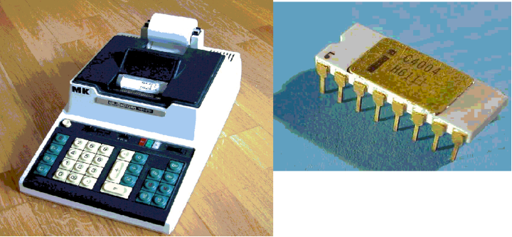
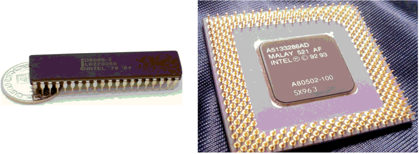
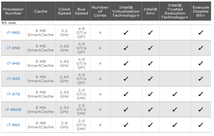
The Intel–4004
September
1969 The Japanese company, Busicom, asked Intel to manufacture
a set of twelve custom chips for a proposed electronic calculator.
Ted
Hoff of Intel realized that it was possible to design a 4–bit general–purpose
CPU on a single chip. This would do the
job more cheaply and simply.
November
1971 The Intel–4004 chip was
delivered. It had 2300 transistors.
More on the
Intel–4004
The
Intel–4004 was designed to perform arithmetic on a variant of
Packed Decimal values, stored with four bits per decimal digit.
Its
clock speed was 108 kilohertz, which is 0.108 megahertz.
It
could address 128 bytes of program memory and 512 bytes of data memory.
The
Intel–8008 and Intel–8080
When
Intel thought it might be able to use the 4004 in other projects, it offered
to buy back the rights to the chip by refunding the $60,000 it had been paid
to develop it. Busicom quickly agreed.
Intel
then began the design of the Intel–8008, an eight–bit upgrade to the 4004.
When
the Intel–8008 proved so popular, Intel began design of another upgrade.
This was the Intel–8080, released in 1974.
The
Intel–8080 quickly became a mass market item.
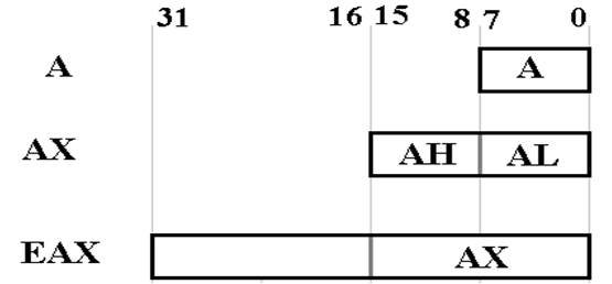
The EAX Register
In
1974, the Intel–8008 had an 8–bit accumulator, called the A register.
In
1978, the Intel–8086 had a 16–bit accumulator, called the AX register.
In
1983, the Intel–80386 had a 32–bit accumulator, called the EAX register.
All
designs had to run Intel–8008 code, thus support the A register.
After
1978, all designs had to run Intel–8086 code, supporting the AX register.
Here
is Intel’s solution to the problem. All
IA–32 code can directly access:
EAX (32 bits), AX (16 bits), AH, or AL (each is 8 bits).
Other Register
Groupings
Grouping 32–bit 16–bit 8–bit
A EAX AX AH and AL
B EBX BX AH
and BL
C ECX CX CH
and CL
D EDX DX DH and DL
Example: Setting the 16–bit register AX to value 0x1234
(hexadecimal)
Intel will call this
number 1234h.
MOV
EAX, 00001234h // Also sets upper 16
bits.
MOV
AX, 1234h // Set only AX
// Upper 16 bits
not affected.
MOV
AH, 12h // Set bits 15 – 8 of EAX
MOV AL, 34h // Set bits 7 – 0 of EAX
There
is no special name for bits 31 – 16 of any register.
More History:
the Intel–8086 and After
1978 The Intel 8086 and related 8088 processors
are released.
Each has 16–bit internal
data registers and busses.
The Intel 8086 had a 16–bit
external data bus.
The Intel 8088 had an 8–bit
external data bus (cheaper).
Each has a 20–bit address bus.
This would allow 1 megabyte
to be addressed.
Bill Gates: “Who would need more than 1 megabyte of
memory?”
Division
of this 1 megabyte (1024 kilobytes = 220 bytes)
640 kilobytes for user program memory
384 kilobytes for system use: graphics memory,
I/O buffers, etc.
More History
1980 The Intel–8087 is announced as a
floating–point coprocessor for
the Intel–8086 and
Intel–8088.
As
a coprocessor, it did not adhere to the Intel–8086 ISA.
The
internal floating–point representation called for 80 bits.
This had a large influence on the IEE–754 floating–point standards.
This
was the first of a line of coprocessors: 80187, 80287, 80387, & 80487.
Later models of the Intel–80486 and all models of the Pentium placed the
floating point processor on the CPU chip, dropping the coprocessor chip.
1982 The
Intel 80186 was announced. It had a
clock speed of 6 MHz.
It was not compatible with
the IBM PC design, so it was not popular.
1982 The
Intel 80286 was announced, with an address space to 24 bits,
for an astounding 16
Megabytes allowed.
(Intel should have jumped to
32–bit addressing, but
had
convincing financial reasons not to do so).
The 80286 originally had a 6
MHz clock.
Still More
History
1983 The
introduction of the Intel–80386, the first of the IA–32 family.
This CPU had 32–bit registers,
32–bit data busses, and a 32–bit address bus.
The 32–bit accumulator was called
the “EAX register”.
The Intel–80386 was introduced with a 16
MHz clock.
It had three memory protection modes:
protected, real, and virtual.
The Intel–80386 is the first of the IA–32
line of processors.
1989 The Intel 80486 is introduced. It was the first of the Intel
microprocessors to contain
one million transistors.
Later variants incorporated the
floating–point processor in the core.
1992 Intel attempts to introduce the Intel
80586.
It could not get a trademark on a
number, so it changed the name
to “Pentium”.
The name “80586” was used briefly
as a generic name for the
Pentium and its clones by
manufacturers such as AMD.
16–Bit and
32–Bit Addressing
Sixteen–bit Addressing
The
Intel 8086 and later use a segmented address system in order to generate
20–bit addresses from 16–bit registers.
Each
of the main address registers was paired with a segment register.
The
IP (Instruction Pointer) is paired
with the CS (Code Segment) register.
The
SP (Stack Pointer) is paired with
the SS (Stack Segment) register.
NOTE: The Intel terminology IP is superior to the
standard name for the
register holding the address
of the next instruction to execute.
The standard name is PC (Program
Counter), so named because
it does not count anything.
The
Intel 8086 used the segment:offset approach to generating a 20–bit address
from a 16–bit segment value and 16–bit offset.
The
steps are as follows.
1. The
16–bit value in the segment register is treated as a 20–bit number
with four leading binary
zeroes. This is one hexadecimal 0.
2. This
20 bit value is left shifted by four, shifting out the high order four
0 bits and shifting in four
low order 0 bits.
This is equivalent to adding
one hexadecimal 0.
3. The
16–bit offset is expanded to a 20–bit number with four leading 0’s
and added to the shifted
segment value. The result is a 20–bit
address.
Example: CS = 0x1234 and IP = 0x2004.
CS with 4 trailing 0’s: 0001 0010 0011 0100 0000 or 0x12340
IP with 4 leading 0’s: 0000 0010 0000 0000 0100 or 0x02004
Effective address: 0001 0100 0011 0100 0100 or 0x14344
Backward
Compatibility in the I/O Busses
Here is a figure
that shows how the PC bus grew from a 20–bit address through
a 24–bit address to a 32–bit address while retaining backward compatibility.
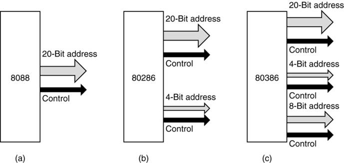
Intel–8086/8088
peripherals could be attached to the external bus of
either an Intel–80286 or Intel–80386.
Intel
80286 peripherals could be attached to an Intel–80386 data bus.
The Intel–80286
Sockets
The
IBM computer designed around the Intel–80286 was called the
IBM PC/AT for “Personal Computer /
Advanced Technology”
Memory Models:
Another Intel–8086 Holdover
Segment–offset
addressing is based on the use of 16–bit offsets.
The
offset is treated as a 16–bit unsigned
integer.
This
allows byte offsets in the range 0 through 65,535, a maximum
size of 64 KB.
If
the code is larger than 64 KB, the CS register must be managed explicitly.
If
the data area is larger than 64 KB, the DS register must be managed.
This
leads to a number of memory models,
seen on early assemblers. These are
based on the size of the code and
the size of the data.
Code Size Data
Size Model to Use
Under 64 KB Under
64 KB Small or Tiny
Over 64KB Under 64 KB Medium
Under 64 KB Over 64 KB Compact
Over 64 KB Over 64 KB Large
The
smaller memory models give rise to code that is more compact and
efficient. Modern code, with 32–bit
addressing, does not require these.
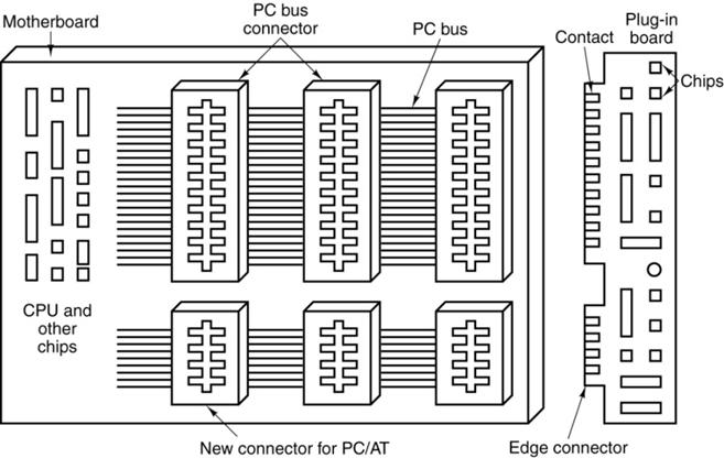
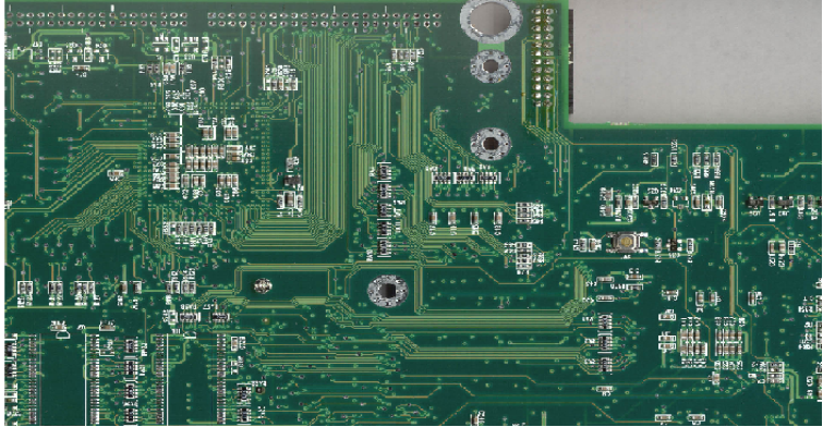
Motherboards
A
computer comprises a number of interconnected components.
Early
designs, for example the PDP–10 from 1968, used wires.
These backplanes were expensive and difficult to manufacture.
This
lead to the creation of the PCB (Printed Circuit Board) or Motheboard.
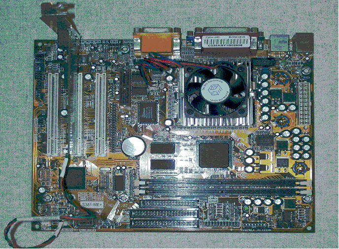
Another
Motherboard
This
motherboard appears to have copper traces.
Note the fan for the CPU.
Sockets and
Slots
Each
is a mechanical component that allows a circuit element (CPU, memory
module, etc.) to be inserted into the motherboard. In the early designs, the
CPU would be connected directly to the motherboard via a socket.
Some
later designs had the CPU mounted in a module with other components
(probably cache memory). That module was
connected via a slot.
The
design of slots and sockets was driven by the CPU pin count.
Intel 8086 Pentium 1
Early Sockets
Here is a table of some of the
early sockets used for the IA–32 series.
|
Socket |
Year |
CPU
families |
Package |
Pin
|
Bus
speed |
|
DIP |
1970s |
Intel 8086, Intel 8088 |
DIP |
40 |
5/10 MHz |
|
Socket
1 |
1989 |
Intel 80486 |
PGA |
169 |
16–50 MHz |
|
Socket
2 |
? |
Intel 80486 |
PGA |
238 |
16–50 MHz |
|
Socket
3 |
1991 |
Intel 80486 |
PGA |
237 |
16–50 MHz |
|
Socket
4 |
? |
Intel Pentium |
PGA |
273 |
60–66 MHz |
|
Socket
5 |
? |
Intel Pentium, AMD K5 |
PGA |
320 |
50–66 MHz |
|
Socket
6 |
? |
Intel 80486 |
PGA |
235 |
? |
|
Socket
7 |
1994 |
Intel Pentium, Intel Pentium |
PGA |
321 |
50–66 MHz |
|
Socket
8 |
1995 |
Intel Pentium Pro |
PGA |
387 |
60–66 MHz |
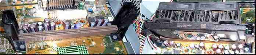
Slots and the
SECC
The
introduction of the Pentium II (Pentium Pro) required a new packaging
method, called SECC (Single–Edged Contact Cartridge).
The
Pentium II had a design yielding significant performance benefits,
but presenting many difficulties in manufacture and testing.
The
answer was a separate circuit board, called a SECC, onto which the
CPU and cache memory would be mounted.
Here is a Pentium 2 in a SECC.

Slot 1
Slot 1 refers to the
physical and electrical specification for the connector
used by some of Intel's microprocessors:
Pentium Pro, Celeron, Pentium II and the Pentium III.
Slot
1 (also Slot1 or SC242) is a slot-type connector with 242 contacts.
Here
are two pictures showing a Slot 1 connection.
The Empty Slot The CPU and Cooling Fans in the Slot
Slot 2 refers to the
physical and electrical specification for the 330-lead Single
Edge Contact Cartridge (or
edge-connector) used by some of Intel's Pentium II
Xeon and certain models of the Pentium III Xeon.
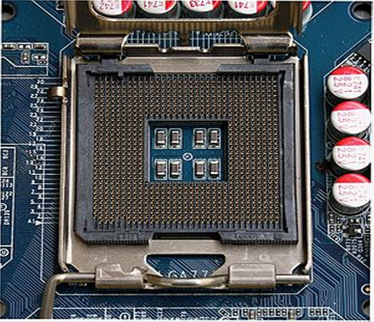
The LGA 775
Socket
Here
is a picture from [R017] of the LGA 775 mounted on some sort of
motherboard. It is used by some of the
Pentium 4 designs.
Back to the
Power Wall
We now revisit the problem that stopped the advance in CPU
clock speeds. It is
called the “power wall”, because the issue was the power emitted by the CPU.
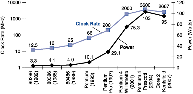
· The design goal for
the late 1990’s and early 2000’s was to drive the clock
rate up. This was done by adding more transistors to a
smaller chip.
· Unfortunately, this
increased the power dissipation of the CPU chip
beyond the capacity of inexpensive
cooling techniques.
Roadmap for CPU Clock Speed: Circa 2005
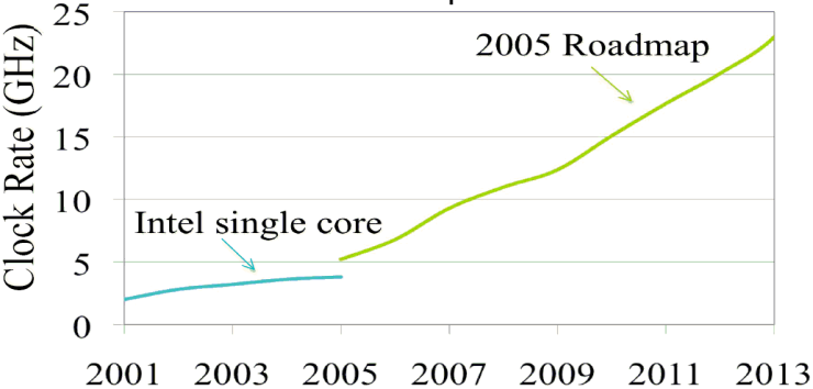
Here is the result of the best
thought in 2005. By 2015, the clock
speed
of the top “hot chip” would be in the 12 – 15 GHz range.
These projections were made purely
on the electrical considerations, such as
circuit density and line size. Ignoring
power issues, these were very reasonable.
The CPU Clock Speed Roadmap (A Few Revisions Later)
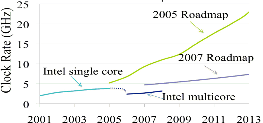
This reflects the practical
experience gained with dense chips that were literally
“hot”; they radiated considerable thermal power and were difficult to cool.
Law of Physics: All electrical power consumed is eventually
radiated as heat.
Cooling
a Faster Single–Core CPU
Here are some solutions to cooling the “hot CPU”.
With coolers such as these, it is possible to “overclock” the CPU; that is,
to run it at a higher clock rate than the commercially released version.
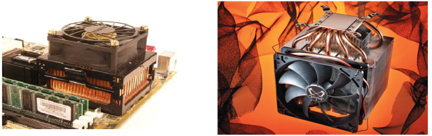
Akasa Copper Heatsink Mugen
2 Cooler
A Google search for “Computer
Cooling Radiators” shows a brisk market
in water cooling units for commodity CPU chips.
The
Intel
The CPU chip (code named “
in the actual clock rate. The fastest
mass–produced chip ran at 3.8 GHz, though
some enthusiasts (called “overclockers”) actually ran the chip at 8.0 GHz.
Upon release, this chip was thought to generate about 40%
more heat per
clock cycle that earlier variants. This
gave rise to the name “PresHot”.
The
which was intended to be scaled up eventually to ten gigahertz. The heat
problems could never be handled, and Intel abandoned the architecture.
The following are adapted from a review of the
·
The
·
The only way to keep it below 60
Celsius (140 F) was to operate it
with the cover off and plenty of ventilation.
·
Even equipped with the massive Akasa
King Copper heat sink (see a
previous slide), the system reached 77 Celsius (171 F) when operating
at 3.8 GHz under full load and shut itself down.
Multicore Chips: The Start of a New Line
Rather than continuing to improve single–program
performance, many
commercial chip manufacturers have adopted a “server mentality”; increase
the throughput of a number of programs running concurrently.
We shall study parallel processing later. At that time, we shall not that the
difficulty lies in keeping all processors doing productive work.
The division of a single problem among a large number of
processors, or the
use of a large number of processors for cooperating tasks, is difficult.
Recall that a multicore
chip is just a CPU chip with multiple processors.
In a server, especially a large one such as the IBM z/10,
there are a large number
of independent processes that do not need to intercommunicate. Allocation of
processors (cores) to such a job mix is almost trivial.
Question: Compare a single
processor operating at 4 GHz to a
dual core processor
with each core operating at 2 GHz.
The dual core processor is likely to consume less power, but
can it do
the same amount of work per unit time as the faster single core processor?
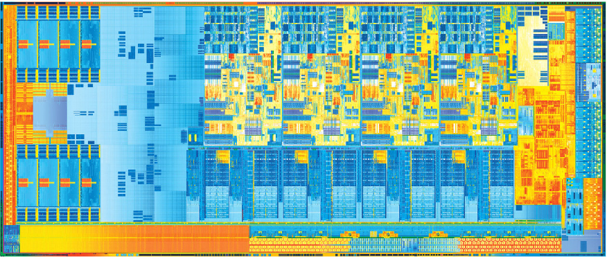
Intel’s Multicore Chip Offerings for 2010
For 2010, Intel Corporation has released a new series of multicore
processors.
Here is a Intel Corp overview of this series.
All of these seem to be quad–core.
Picture of a Modern Quad–Core CPU
Intel’s Rationale
According to Intel, the multi–core technology will
·
permanently alter the course of
computing as we know it,
·
provide new levels of energy
efficient performance,
·
deliver full parallel execution of
multiple software threads, and
·
reduce the amount of electrical
power to do the computations.
The
current technology provides for one, two, four, or eight cores in
a single processor.
Intel
expects to have available soon single processors with several tens
of cores, if not one hundred.
This
new technology seems to be targeted at the commercial desktop machine,
which can “run several demanding modern applications at once”.
At
present, there are little hard data on multicore machines.
What we have mostly is marketing hype.
That might change soon.