Design of the
ALU
Adder, Logic, and the Control Unit
This lecture
will finish our look at the CPU and ALU of the computer.
Remember:
1. The
ALU performs the arithmetic and logic operations.
2. The
control unit causes the CPU to do what the program says to do.
We
begin by reviewing the binary adder, and discussing ways to speed it up.
The Binary Adder
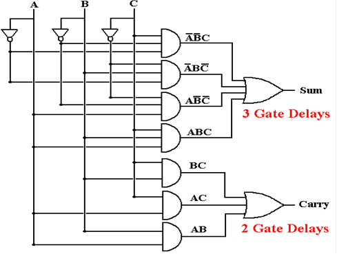
Here
is a diagram of the full adder we discussed in the previous lecture.
Note
the timings on the output.
After the input is valid, the carry out
is valid two gate delays later.
the
sum is valid three gate delays later.
Another Full
Adder Implementation
Here
is an implementation in Rob Williams’s book.
Note the timings.
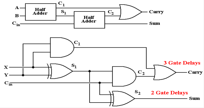
The
sum is faster, but the carry–out is slower.
The carry–out timing is more important.
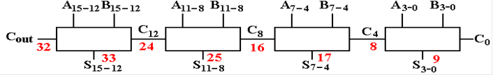
A Four–Bit
Ripple–Carry Adder
Here
is the symbol we often use for a full adder.
It has three inputs and two outputs.
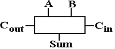
Here
is a four–bit adder built from these elements.
It has the timings added.
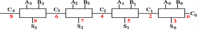
Note
that the correct value of the carry “ripples” from right to left.
The sum bit is valid only after nine gate delays.
NOTE: It is the time to propagate the carry values
that makes this slow.
If it were not for this
problem with the carry, all values would be valid at T = 3.
For that reason, we favor
designs that produce the carry bit more quickly.
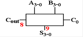
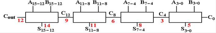
The Four–Bit
Adder as a Building Block
Here
is a block diagram of the four–bit adder with its timings.
Here
is a 16–bit adder built from four of these building blocks. Note its timings.
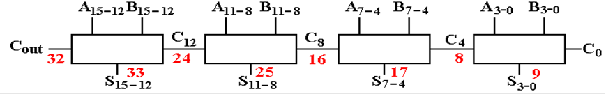
Consider
an N–bit adder. The high order sum bit
is SN–1,
produced in 2·(N – 1) + 3 gate delays.
In
general, a ripple–carry adder produces a valid N–bit sum after 2·N + 1 gate
delays.
A
32–bit sum requires 65 gate delays, about 65 to 130 nanoseconds. Much too slow!
The Carry
Look–Ahead Adder
Modern
adders achieve greater speed by generating the carry–in to higher bits more
quickly.
The
standard design is a variant of the carry look–ahead adder.
Here
is a taste of what that design does. In
our ripple–carry adder, the carry bits are
generated independently and propagate.
This takes time.
Here: C1 = A0·B0 + A0·C0 +
B0·C0
= A0·B0 +
(A0 + B0)·C0
Likewise: C2 = A1·B1 + (A1 +
B1)·C1 // Wait 2 gate delays to get C1
right.
Why
not C2 = A1·B1 +
(A1 + B1)·[A0·B0 +
(A0 + B0)·C0 ]
= A1·B1 +
(A1 + B1)·A0·B0·C0 +
(A1 + B1)·(A0 + B0)·C0
This
is messy, but it is achievable in three gate delays, not the four listed above.
The Carry
Look–Ahead Adder (Part 2)
We
can extend these equations to any carry bit, but let’s focus on four bits.
The
notation is much simpler if we adopt standard notation: Gk = Ak · Bk
Pk = Ak + Bk
We
can now write the above two equations (and the two others) as
C1 = G0 + P0·C0
C2 = G1 + P1·G0 +
P1·P0·C0
C3 = G2 + P2·G1 +
P2·P1·G0 +
P2·P1·P0·C0
C4 = G3 + P3·G2 +
P3·P2·G1 +
P3·P2·P1·G1 +
P3·P2·P1·P0·C0
This may look
messy, but note the following
1. Each
value of Gk and Pk
can be computed independently, at the same time,
in only one gate delay.
2. Each
of C1, C2, C3, and C4 can be
calculated in two more gate delays,
for a total of three gate
delays for each.
3. Using
Rob Williams’s circuit Sk = [Ak Å Bk] Å Ck, the sum can
be computed two gate
delays after the carry is valid. Each
sum in 5 gate delays.
Comparison of
Ripple Carry and Carry Look–Ahead
This slide shows
the relative timings of the two designs for a four–bit adder.
The timings are
identical for a circuit that both adds and subtracts.
The ripple–carry
adder
The carry
look–ahead adder.
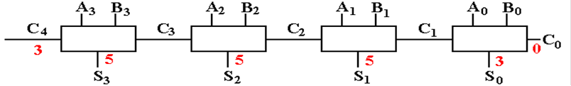
This illustrates
a classic design trick, used constantly in the development of modern
computers. Adding more hardware enables
tricks to speed up the circuitry.
A More Realistic
Design
Theoretically,
the carry look–ahead adder can compute a 16–bit sum in 5 gate delays.
Such a design
would require a few hundred basic gates.
It would be hard to farbricate.
A more realistic
design would be based on connecting four–bit adders.
Here is the comparison.
The ripple–carry
design.
The carry
look–ahead design.
This is about
2.4 times as fast as the original.
Standard design tricks can be applied
to make it again twice as fast, thus five times as fast as the ripple–carry
adder.
Controlling the
ALU
The Control Unit (CU) is the part of the
CPU that issues signals to cause the
computer to do what the program instructs it to do.
In the next few
slides, we shall investigate how control signals are applied to the
Arithmetic Logic Unit (ALU).
In each of the
next few slides, the ALU will be considered to have two inputs (A and B)
and one output (C). The figure below
uses the standard symbol for an ALU.
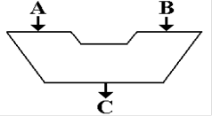
We begin with a
very simple three–function ALU and develop the design from there.
1. C
= A ·
B
2. C
= A + B
3. C
= A Å
B
A real ALU must
do more than this, but we just want to get an idea of its control.
Three Control
Signals for Three Functions
A control signal
is a binary signal with two values: asserted and not asserted.
These control signals are asserted high; TRUE (1) = Asserted and FALSE (0) =
Not asserted.
A control signal
is often labeled by the action it enables: here and, not, and xor.
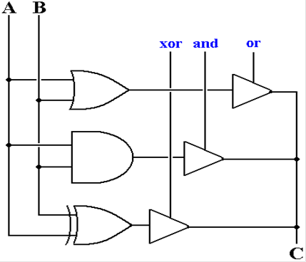
If one of these
signals is asserted, the corresponding function is placed on line C.
If more than one signal is asserted, the circuit malfunctions.
Encoding the
Control Signals
One way to
insure that two or more control signals are not asserted at the same time is
to specify a binary code for every action.
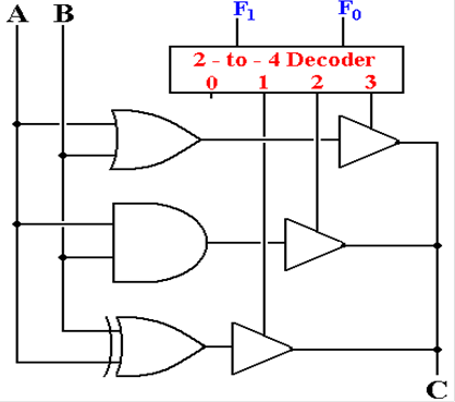
The codes are 00 Do
nothing
01 Exclusive OR
10 AND
11 OR
The “Do Nothing”
Option
Note that output
0 of the decoder is not attached to anything.
When the
function code is 00, the ALU does not place anything on its output.
Why not specify another useful function, such as the logical NOT?
In order to see
the answer, we must remember that the ALU must function in context.
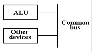
Here, there are
a number of devices that can put output onto the common bus.
When another device is called on to assert data on the bus, the ALU must not
assert anything.
The Shift Unit
The shift unit is part of the ALU. Its function is to shift data.
There are three
types of shifts:
Logical shifts
Arithmetic shifts
Circular shifts
The shift
operations are very useful, though they may seem a bit strange at first.
Shift operations
do not correspond to any logical operators.
Shift operations
do not directly correspond to any arithmetic operators,
though the arithmetic shifts can be made to be equivalent to multiplication
and division by powers of two.
The shift
operations just move bits within a register.
Double shift
operations move bits within a pair of registers.
NOTE: For simplicity, we use 8–bit examples.
We assume that bit 7 is
the sign bit if the 8–bit example illustrates signed integers.
Simple Logical
Shifts
Here are some
examples of simple logical shifts, in which a 0 is shifted into
the vacated “spot”.
The original
value in binary: 1001 0110
The original value right shifted one place: 0100 1011
The original value right shifted two places 0010 0101
The original
value in binary: 1001 0110
The original value left shifted one place: 0010 1100
The original value left shifted two places 0101 1000
Here are two
single–bit logical shifts.
Logical
Left Shift Logical
Right Shift
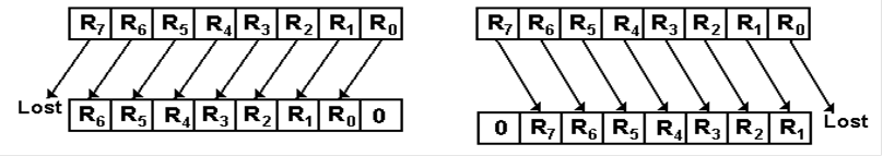
Note that the
sign bit can be changed by a logical shift
Arithmetic
Shifts
Arithmetic
shifts are similar to logical, except that the sign bit is preserved.
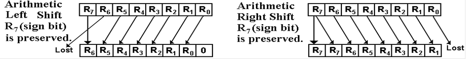
Here are two
illustrations of a sequence of arithmetic shifts on positive and negative numbers.
Right Arithmetic Shift Left
Arithmetic Shift
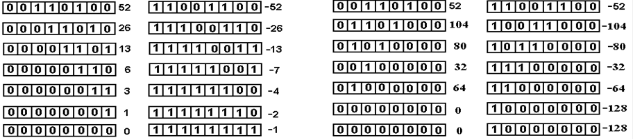
The right shift
does resemble division by 2 until one gets to either 1 or –1.
The left shift
occasionally resembles multiplication by 2.
Note 2·104 = 208 = 128 + 80.
If the value goes outside of the range [–128, 127], shifting is not equivalent
to multiplication.
Circular Shifts
Here the bits
are wrapped around; nothing is lost.
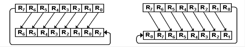
In this example,
a left circular shift by N bits is the same as a right circular shift by (8 –
N).
For 32 bits, the
equivalence is N and (32 – N).
Double Shifts
Here is an
arithmetic right double shift as might be implemented on the IBM Mainframe.
In this
architecture
1. Integer
registers are numbered 0 through 15, and identified by number.
2. Double
register shifts are applied to even–odd pairs, such as (8, 9) or (10, 11).
If the pair below were (4,
5), the instruction might be SRDA 4, 1.
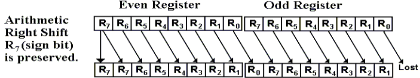
Most
architectures support six types of double shifts: three double left shifts
and three double right shifts.
Each of left and
right can be logical, arithmetic, or circular.
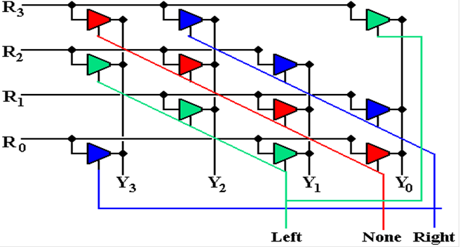
A Four–Bit Circular
Barrel Shifter
A barrel shifter
can do all of the shifting in one step.
An N–bit barrel
shifter is implemented with N2 tri–state buffers.
For this reason, it is hard to draw large barrel shifters.
Here is the
example, with 3 options: no shift, circular left by 1, and circular right by 1.