Views of
Memory
We begin with a number of views of computer memory and
comment on their use.
The simplest view of memory is that presented at the
ISA (Instruction Set Architecture)
level. At this level, memory is a
monolithic addressable unit.
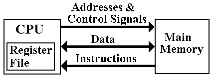
At this level, the memory is a repository for data and
instructions, with no internal
structure apparent. For some very
primitive computers, this is the actual structure.
In this view, the CPU issues addresses and control
signals. It receives instructions
and data from the memory and writes data back to the memory.
This is the view that suffices for many high–level
language programmers.
In no modern architecture does the CPU write
instructions to the main memory.
The Logical
Multi–Level View of Memory
In a course such as this, we want to investigate the
internal memory structures
that allow for more efficient and secure operations.
The logical view for this course is a three–level view
with
cache memory, main memory, and
virtual memory.
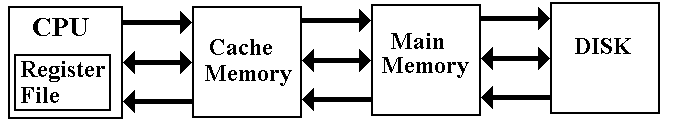
The primary memory is backed by a “DASD” (Direct
Access Storage Device),
an external high–capacity device.
While “DASD” is a name for a device that meets certain
specifications, the standard
disk drive is the only device currently in use that “fits the bill”. Thus DASD = Disk.
This is the view we shall take when we analyze cache
memory.
A More
Realistic View of Multi–Level Memory
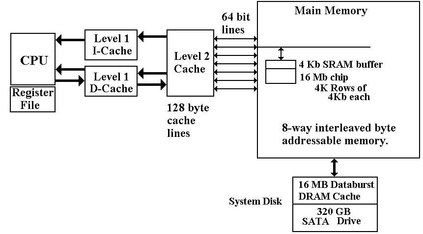
Generic
Primary / Secondary Memory
This
lecture covers two related subjects: Virtual
Memory and Cache Memory.
The
two subjects have much in common; their theoretical basis is the same.
In
each case, we have a fast primary memory
backed by a bigger secondary memory.
The “actors” in the two cases
are as follows:
Technology Cache Memory Virtual Memory
Faster Memory SRAM
Cache DRAM Main Memory
Slower Memory DRAM
Main Memory Disk
Block Name Block Page
Block Fits into Cache
Line Page Frame
Block Size 32 to 128 bytes 512
to 4,096 bytes
Always
a multiple of 512.
NOTE: The logical block of secondary
memory is always the same size as its frame
Cache memory: A 32–byte cache line implies memory blocks
of 32 bytes.
Virtual memory: A 512–byte page frame implies pages of 512
bytes.
Effective
Access Time
The discussion of effective access time should be
considered in the generic model of
primary (faster) memory vs. secondary (slower and larger) memory.
Faster memory Access
time = TP (Primary Time).
Slower memory Access
time = TS (Secondary Time).
Always we have TP £ 0.10 · TS. For virtual memory TP £ 0.00010 · TS.
Effective
Access Time: TE = h · TP + (1 – h) · TS, where h (the
primary hit rate) is
the fraction of memory accesses satisfied by the primary memory; 0.0 £ h £ 1.0.
This formula does extend
to multi–level caches. For example a
two–level cache has
TE = h1 · T1 + (1 – h1) · h2 · T2 + (1 – h1) · (1 – h2) · TS.
NOTATION WARNING: In some contexts, the DRAM main memory is called
“primary memory”. I never use that
terminology when discussing multi–level memory.
Examples:
Cache Memory
Suppose a single cache
fronting a main memory, which has 80 nanosecond access time.
Suppose the cache memory
has access time 10 nanoseconds.
If the hit rate is 90%,
then TE = 0.9 · 10.0 + (1 – 0.9) · 80.0
` = 0.9 · 10.0 + 0.1 · 80.0 = 9.0 + 8.0 = 17.0 nsec.
If the hit rate is 99%,
then TE = 0.99 · 10.0 + (1 – 0.99) · 80.0
` = 0.99 · 10.0 + 0.01 · 80.0 = 9.9 + 0.8 = 10.7 nsec.
Suppose a L1 cache with T1
= 4 nanoseconds and h1 = 0.9
Suppose a L2 cache with T2 = 10 nanoseconds
and h2 = 0.99
This is defined to be the number of hits on references that are a miss at L1.
Suppose a main memory with TS = 80.0
TE = h1
· T1 + (1 – h1) · h2
· T2 + (1 – h1) · (1 – h2)
· TS.
= 0.90 · 4.0 + 0.1 · 0.99 · 10.0 + 0.1 · 0.01 · 80.0
= 0.90 · 4.0 + 0.1 · 9.9 + 0.1 · 0.80
= 3.6 + 0.99 + 0.08 = 4.67 nanoseconds.
Note that with these hit
rates, only 0.1 · 0.01 = 0.001 = 0.1% of the memory
references are handled by the much slower main memory.
Example:
Virtual Memory
Suppose a main memory with access time of 80
nanoseconds being backed by a
disk with access time 10 milliseconds (10,000,000 nanoseconds).
Suppose 1,024–byte disk blocks and a hit rate of .9981
( 1,022 / 1,024).
Then, TE =
h · TP + (1 – h) · TS
=
0.9981 · 80 + 0.0019 · 10,000,000
=
79.8 + 19,000 = 19,080 nanoseconds
(approximately).
Suppose 1,024–byte disk blocks and a hit rate of
.9999.
Then, TE =
h · TP + (1 – h) · TS
=
0.9999 · 80 + 0.0001 · 10,000,000
=
80.0 + 1,000 = 1,080 nanoseconds
(approximately).
One can easily see that effective virtual memory is
based on having a very high hit rate.
The
Principle of Locality
It is the principle
of locality that makes this multi–level memory hierarchy work.
There are a number of ways to state this principle of
locality, which refers to the
observed tendency of computer programs to issue addresses in a small range.
Temporal Locality if a program references an address,
it
will likely address it again.
Spatial Locality if a program references an address,
the
next address issues will likely be “close”.
Sequential Locality programs tend to issue sequential
addresses,
executing
one instruction after another.
In 1968, Peter J. Denning, noted what he called the “working set”, which refers
to the tendency of computer programs to spend considerable periods of time
issuing
addresses within a small range.
In the Virtual Memory arena, this causes a small
number of pages to be read into the
main memory and used continuously for a significant time. It is this set of pages
that is precisely the working set.
Generic
Primary / Secondary Memory View
A small fast expensive
memory is backed by a large, slow, cheap memory.
Memory references are
first made to the smaller memory.
1. If
the address is present, we have a “hit”.
2. If
the address is absent, we have a “miss” and must transfer the addressed
item from the slow
memory. For efficiency, we transfer as a
unit the block
containing the addressed
item.
The mapping of the
secondary memory to primary memory is “many to one” in that
each primary memory block can contain a number of secondary memory addresses.
To compensate for each of
these, we associate a tag with each
primary block.
For example, consider a
byte–addressable memory with 24–bit addresses and 16 byte
blocks. The memory address would have
six hexadecimal digits.
Consider the 24–bit address
0xAB7129. The block containing that
address is every
item with address beginning with 0xAB712: 0xAB7120, 0xAB7121, … , 0xAB7129,
0xAB712A, … 0xAB712F.
The primary block would
have 16 entries, indexed 0 through F. It
would have the 20–bit
tag 0XAB712 associated with the block, either explicitly or implicitly.
Valid and
Dirty Bits
Consider a cache line
with eight bytes and a tag field.
|
Tag \ Offset |
0 |
1 |
2 |
3 |
4 |
5 |
6 |
7 |
|
0 |
0 |
0 |
0 |
0 |
0 |
0 |
0 |
0 |
What does this cache line
contain?
1. It
contains nothing as data have not been copied from main memory.
2. It
contains the first 8 bytes of an all–zero array at address 0.
How
do we know which it is? We need some
tags associated with each cache line.
At
system start–up, the faster memory contains no valid data, which are copied as
needed from the slower memory.
Each block would have
three fields associated with it
The tag field (discussed
above) identifying the memory addresses
contained
Valid bit set
to 0 at system start–up.
set to 1 when valid data have been copied into the block
Dirty bit set
to 0 at system start–up.
set to 1 whenever the CPU writes to the faster memory
set to 0
whenever the contents are copied to the slower memory.
Associative
Memory
Associative memory is
“content addressable” memory. The contents
of the memory
are searched in one memory cycle.
Consider an array of 256
entries, indexed from 0 to 255 (or 0x0 to 0xFF).
Suppose that we are
searching the memory for entry 0xAB712.
Normal memory would be
searched using a standard search algorithm, as learned
in beginning programming classes.
If the memory is unordered, it
would take on average 128 searches to find an item.
If the memory is ordered, binary
search would find it in 8 searches.
Associative memory would find the item in one search.
Think of the control circuitry
as “broadcasting” the data value (here oxAB712) to all memory cells at the same
time.
If one of the memory cells has the value, it raises a Boolean flag and the item
is found.
We do not consider
duplicate entries in the associative memory.
This can be handled
by some rather straightforward circuitry, but is not done in associative
caches.
Associative
Cache
We now focus on cache
memory, returning to virtual memory only at the end.
Primary memory = Cache Memory (assumed to be one level)
Secondary memory = Main DRAM
Assume
a number of cache lines, each holding 16 bytes.
Assume a 24–bit address.
The simplest arrangement
is an associative cache. It is also the hardest to implement.
Divide
the 24–bit address into two parts: a 20–bit tag and a 4–bit offset.
|
Bits |
23 – 4 |
3 – 0 |
|
Fields |
Tag |
Offset |
A cache line in this
arrangement would have the following format.
|
D bit |
V Bit |
Tag |
16 indexed entries |
|
0 |
1 |
0xAB712 |
M[0xAB7120] … M[0xAB712F] |
The placement of the 16 byte
block of memory into the cache would be determined by
a cache line replacement policy. The policy would probably be as follows:
1. First,
look for a cache line with V = 0. If one
is found, then it is “empty”
and available, as nothing
is lost by writing into it.
2. If all cache
lines have V = 1, look for one with D = 0.
Such a cache line
can be overwritten without
first copying its contents back to main memory.
Direct–Mapped
Cache
This
is simplest to implement, as the cache line index is determined by the address.
Assume
256 cache lines, each holding 16 bytes.
Assume a 24–bit address.
Recall that 256 = 28, so that we need eight bits to select the cache
line.
Divide
the 24–bit address into three fields: a 12–bit explicit tag, an 8–bit line
number,
and a 4–bit offset within the cache line.
Note that the 20–bit memory tag is divided
between the 12–bit cache tag and 8–bit line number.
|
Bits |
23 – 12 |
11 – 4 |
3 – 0 |
|
Cache View |
Tag |
Line |
Offset |
|
Address View |
Block Number |
Offset |
|
Consider the address 0xAB7129.
It would have
Tag = 0xAB7
Line = 0x12
Offset = 0x9
Again,
the cache line would contain M[0xAB7120] through
M[0xAB712F].
The cache line would also have a V bit and a D bit (Valid and Dirty bits).
This
simple implementation often works, but it is a bit rigid. An design that is a
blend
of the associative cache and the direct mapped cache might be useful.
Set–Associative
Caches
An
N–way set–associative cache uses
direct mapping, but allows a set of N memory
blocks to be stored in the line. This
allows some of the flexibility of a fully associative
cache, without the complexity of a large associative memory for searching the
cache.
Suppose
a 2–way set–associative implementation of the same cache memory.
Again
assume 256 cache lines, each holding 16 bytes.
Assume a 24–bit address.
Recall that 256 = 28, so that we need eight bits to select the cache
line.
Consider
addresses 0xCD4128 and 0xAB7129. Each
would be stored in cache line
0x12. Set 0 of this cache line would
have one block, and set 1 would have the other.
|
Entry 0 |
Entry 1 |
||||||
|
D |
V |
Tag |
Contents |
D |
V |
Tag |
Contents |
|
1 |
1 |
0xCD4 |
M[0xCD4120] to M[0xCD412F] |
0 |
1 |
0xAB7 |
M[0xAB7120] to M[0xAB712F] |