Views of
Memory
We begin with a number of views of computer memory and
comment on their use.
The simplest view of memory is that presented at the
ISA (Instruction Set Architecture)
level.
At this level, memory is a monolithic addressable unit.
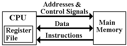
At this level, the memory is a repository for data and
instructions, with no internal
structure apparent. For some very
primitive computers, this is the actual structure.
In this view, the CPU issues addresses and control
signals. It receives instructions
and data from the memory and writes data back to the memory.
This is the view that suffices for many high–level
language programmers.
In no modern architecture does the CPU write
instructions to the main memory.
The Logical
Multi–Level View of Memory
In a course such as this, we want to investigate the
internal memory structures that
allow for more efficient and secure operations.
The logical view for this course is a three–level view
with
cache memory, main memory, and
virtual memory.
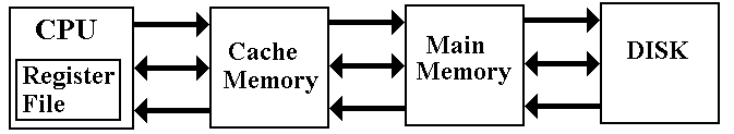
The primary memory is backed by a “DASD” (Direct
Access Storage Device), an
external high–capacity device.
While “DASD” is a name for a device that meets certain
specifications, the standard
disk drive is the only device currently in use that “fits the bill”. Thus DASD = Disk.
This is the view we shall take when we analyze cache
memory.
A More
Realistic View of Multi–Level Memory
Generic
Primary / Secondary Memory
This
lecture covers two related subjects: Virtual
Memory and Cache Memory.
In
each case, we have a fast primary memory backed by a bigger secondary memory.
The “actors” in the two cases
are as follows:
Technology Primary Memory Secondary Memory Block
Cache Memory SRAM
Cache DRAM Main Memory Cache Line
Virtual Memory DRAM
Main Memory Disk Memory Page
Access Time TP
(Primary Time) TS
(Secondary Time)
Effective
Access Time: TE = h · TP + (1 – h) · TS, where h (the
primary hit rate) is
the fraction of memory accesses satisfied by the primary memory; 0.0 £ h £ 1.0.
This formula does extend
to multi–level caches. For example a
two–level cache has
TE = h1 · T1 + (1 – h1) · h2 · T2 + (1 – h1) · (1 – h2) · TS.
NOTATION WARNING: In some contexts, the DRAM main memory is called
“primary memory”. I never use that
terminology when discussing multi–level memory.
Examples:
Cache Memory
Suppose a single cache
fronting a main memory, which has 80 nanosecond access time.
Suppose the cache memory
has access time 10 nanoseconds.
If the hit rate is 90%,
then TE = 0.9 · 10.0 + (1 – 0.9) · 80.0
` = 0.9
· 10.0 + 0.1 · 80.0 = 9.0 + 8.0 = 17.0 nsec.
If the hit rate is 99%,
then TE = 0.99 · 10.0 + (1 – 0.99) · 80.0
` = 0.99
· 10.0 + 0.01 · 80.0 = 9.9 + 0.8 = 10.7 nsec.
Suppose a L1 cache with T1
= 4 nanoseconds and h1 = 0.9
Suppose a L2 cache with T2 = 10 nanoseconds and h2 = 0.99
This is defined to be the number of hits on references that are a miss at L1.
Suppose a main memory with TS = 80.0
TE = h1
· T1 + (1 – h1) · h2
· T2 + (1 – h1) · (1 – h2)
· TS.
= 0.90 · 4.0 + 0.1 · 0.99 · 10.0 + 0.1 · 0.01 · 80.0
= 0.90 · 4.0 + 0.1 · 9.9 + 0.1 · 0.80
= 3.6 + 0.99 + 0.08 = 4.67 nanoseconds.
Note that with these hit
rates, only 0.1 · 0.01 = 0.001 = 0.1% of the memory references
are handled by the much slower main memory.
Precise
Definition of Virtual Memory
Virtual memory has a common
definition that so frequently represents its actual
implementation that we may use it.
However, I shall give its precise definition.
Virtual
memory is a mechanism for translating logical
addresses (as issued by an
executing program) into actual physical memory
addresses.

This definition alone
provides a great advantage to an Operating
System, which can
then allocate processes to distinct physical memory locations according to some
optimization.
Secondary Storage
Although this is a precise
definition, virtual memory has always been implemented
by pairing a fast DRAM Main Memory with a bigger, slower “backing store”. Originally,
this was magnetic drum memory, but it soon became magnetic disk memory.
The invention of time–sharing operating systems introduced
another variant of VM,
now part of the common definition. A
program and its data could be “swapped out”
to the disk to allow another program to run, and then “swapped in” later to
resume.
Common
(Accurate) Definition of Virtual Memory
Virtual memory allows the
program to have a logical address space much larger than
the computers physical address space. It
maps logical addresses onto physical addresses
and moves “pages” of memory between
disk and main memory to keep the program running.
An address space is the range of addresses, considered as unsigned
integers, that can
be generated. An N–bit address can
access 2N items, with addresses 0 … 2N – 1.
16–bit address 216
items 0 to 65535
20–bit address 220 items 0 to 1,048,575
32–bit address 232 items 0 to 4,294,967,295
In all modern
applications, the physical address space is no larger than the logical
address space. It is often somewhat
smaller than the logical address space.
As
examples, we use a number of machines with 32–bit logical address spaces.
Machine Physical Memory Logical Address Space
VAX–11/780 16 MB 4 GB (4, 096 MB)
Pentium (2004) 128 MB 4
GB
Desktop Pentium 512 MB 4
GB
Server Pentium 4 GB 4
GB
NOTE: The MAR structure usually allows the two
address spaces to be equal.
Generic Primary
/ Secondary Memory View
A small fast expensive
memory is backed by a large, slow, cheap memory.
Memory references are
first made to the smaller memory.
1. If
the address is present, we have a “hit”.
2. If
the address is absent, we have a “miss” and must transfer the addressed
item from the slow
memory. For efficiency, we transfer as a
unit the block
containing the addressed
item.
The mapping of the
secondary memory to primary memory is “many to one” in that
each primary memory block can contain a number of secondary memory addresses.
To compensate for each of
these, we associate a tag with each
primary block.
For example, consider a
byte–addressable memory with 24–bit addresses and 16 byte
blocks. The memory address would have
six hexadecimal digits.
Consider the 24–bit address 0xAB7129. The block containing that address is
every item with address beginning with 0xAB712: 0xAB7120, 0xAB7121, … ,
0xAB7129, 0xAB712A, … 0xAB712F.
The primary block would
have 16 entries, indexed 0 through F. It
would have the
20–bit tag 0XAB712 associated with the block, either explicitly or implicitly.
Valid and
Dirty Bits
At system start–up, the
faster memory contains no valid data, which are copied as
needed from the slower memory.
Each block would have
three fields associated with it
The tag field (discussed
above) identifying the memory addresses
contained
Valid bit set
to 0 at system start–up.
set to 1
when valid data have been copied into the block
Dirty bit set
to 0 at system start–up.
set to 1 whenever
the CPU writes to the faster memory
set to 0
whenever the contents are copied to the slower memory.
Associative
Memory
Associative memory is
“content addressable” memory. The
contents of the memory
are searched in one memory cycle.
Consider an array of 256
entries, indexed from 0 to 255 (or 0x0 to 0xFF).
Suppose that we are
searching the memory for entry 0xAB712.
Normal memory would be
searched using a standard search algorithm, as learned
in beginning programming classes.
If the memory is unordered, it
would take on average 128 searches to find an item.
If the memory is ordered, binary
search would find it in 8 searches.
Associative memory would find the item in one search.
Think of the control circuitry
as “broadcasting” the data value (here oxAB712) to all memory cells at the same
time.
If one of the memory cells has the value, it raises a Boolean flag and the item
is found.
We do not consider
duplicate entries in the associative memory.
This can be handled
by some rather straightforward circuitry, but is not done in associative
caches.
Associative
Cache
We now focus on cache
memory, returning to virtual memory only at the end.
Primary memory = Cache Memory (assumed to be one level)
Secondary memory = Main DRAM
Assume
a number of cache lines, each holding 16 bytes.
Assume a 24–bit address.
The simplest arrangement
is an associative cache. It is also the hardest to implement.
Divide
the 24–bit address into two parts: a 20–bit tag and a 4–bit offset.
|
Bits |
23 – 4 |
3 – 0 |
|
Fields |
Tag |
Offset |
A cache line in this
arrangement would have the following format.
|
D bit |
V Bit |
Tag |
16 indexed entries |
|
0 |
1 |
0xAB712 |
M[0xAB7120] … M[0xAB712F] |
The placement of the 16 byte
block of memory into the cache would be determined
by a cache line replacement policy. The policy would probably be as follows:
1. First,
look for a cache line with V = 0. If one
is found, then it is “empty”
and available, as nothing
is lost by writing into it.
2. If all cache
lines have V = 1, look for one with D = 0.
Such a cache line
can be overwritten without
first copying its contents back to main memory.
Direct–Mapped
Cache
This
is simplest to implement, as the cache line index is determined by the address.
Assume
256 cache lines, each holding 16 bytes.
Assume a 24–bit address.
Recall that 256 = 28, so that we need eight bits to select the cache
line.
Divide
the 24–bit address into three fields: a 12–bit explicit tag, an 8–bit line
number,
and a 4–bit offset within the cache line.
Note that the 20–bit memory tag is divided
between the 12–bit cache tag and 8–bit line number.
|
Bits |
23 – 12 |
11 – 4 |
3 – 0 |
|
Cache View |
Tag |
Line |
Offset |
|
Address View |
Block Number |
Offset |
|
Consider the address 0xAB7129.
It would have
Tag = 0xAB7
Line = 0x12
Offset = 0x9
Again,
the cache line would contain M[0xAB7120] through M[0xAB712F].
The cache line would also have a V bit and a D bit (Valid and Dirty bits).
This
simple implementation often works, but it is a bit rigid. An design that is a
blend of the associative cache and the direct mapped cache might be useful.
Set–Associative
Caches
An
N–way set–associative cache uses
direct mapping, but allows a set of N memory
blocks to be stored in the line. This
allows some of the flexibility of a fully associative
cache, without the complexity of a large associative memory for searching the
cache.
Suppose
a 2–way set–associative implementation of the same cache memory.
Again
assume 256 cache lines, each holding 16 bytes.
Assume a 24–bit address.
Recall that 256 = 28, so that we need eight bits to select the cache
line.
Consider
addresses 0xCD4128 and 0xAB7129. Each
would be stored in cache line
0x12. Set 0 of this cache line would
have one block, and set 1 would have the other.
|
Entry 0 |
Entry 1 |
||||||
|
D |
V |
Tag |
Contents |
D |
V |
Tag |
Contents |
|
1 |
1 |
0xCD4 |
M[0xCD4120] to M[0xCD412F] |
0 |
1 |
0xAB7 |
M[0xAB7120] to M[0xAB712F] |
Virtual
Memory (Again)
Suppose
we want to support 32–bit logical addresses in a system in which physical
memory is 24–bit addressable.
We
can follow the primary / secondary memory strategy seen in cache memory.
We shall see this again, when we study virtual memory in a later lecture.
For
now, we just note that the address structure of the disk determines the
structure
of virtual memory. Each disk stores data
in blocks of 512 bytes, called sectors.
In
some older disks, it is not possible to address each sector directly. This is due to
the limitations of older file organization schemes, such as FAT–16.
FAT–16
used a 16–bit addressing scheme for disk access. Thus 216 sectors could be
addressed. Since each sector contained 29
bytes, the maximum disk size under
“pure FAT–16” is 225 bytes = 25 · 220 bytes = 32 MB.
To
allow for larger disks, it was decided that a cluster of 2K sectors
would be the
smallest addressable unit. Thus one
would get clusters of 1,024 bytes, 2,048 bytes, etc.
Virtual
memory transfers data in units of clusters, the size of which is system
dependent.
Examples of
Cache Memory
We
need to review cache memory and work some specific examples.
The
idea is simple, but fairly abstract. We
must make it clear and obvious.
While
most of this discussion does apply to pages in a Virtual Memory system,
we shall focus it on cache memory.
To review, we consider the main
memory of a computer. This memory might
have
a size of 384 MB, 512 MB, 1GB, etc. It
is divided into blocks of size 2K bytes,
with K > 2.
In
general, the N–bit address is broken into two parts, a block tag and an offset.
The most significant (N –
K) bits of the address are the block tag
The least significant K
bits represent the offset within the block.
We
use a specific example for clarity.
byte addressable memory
a 24–bit address
cache block size of 16
bytes, so the offset part of the address is K = 4 bits.
Remember
that our cache examples use byte addressing for simplicity.
EXAMPLE: The
Address 0xAB7129
In
our example, the address layout for main memory is as follows:
Divide
the 24–bit address into two parts: a 20–bit tag and a 4–bit offset.
|
Bits |
23 – 4 |
3 – 0 |
|
Fields |
Tag |
Offset |
Let’s examine the sample
address in terms of the bit divisions above.
|
Bits: |
23 – 20 |
19 – 16 |
15 – 12 |
11 – 8 |
7 – 4 |
3 – 0 |
|
Hex Digit |
A |
B |
7 |
1 |
2 |
9 |
|
Field |
0xAB712 |
0x09 |
||||
So,
the tag field for this block contains the value 0xAB712.
The
tag field of the cache line must also contain this value, either explicitly or
implicitly. More on this later.
Remember: It is the
cache line size that determines the size of the blocks in
main memory. They must be the same size, here 16 bytes.
What Does
The Cache Tag Look Like?
All
cache memories are divided into a number of cache lines. This number is also a
power of two, usually between 256 = 28 and 216 (for
larger L2 caches).
Our
example used in this lecture calls for 256 cache lines.
Associative Cache
As
a memory block can go into any available cache line, the cache tag must
represent
the memory tag explicitly: Cache Tag =
Block Tag. In our example, it is
0xAB712.
Direct Mapped and Set–Associative Cache
For
any specific memory block, there is exactly one cache line that can contain it.
Suppose
an N–bit address space. 2L
cache lines, each of 2K bytes.
|
Address Bits |
(N – L – K) bits |
L bits |
K bits |
|
Cache Address |
Cache Tag |
Cache Line |
Offset |
|
Memory Address |
Memory Block Tag |
Offset |
|
To retrieve the memory block
tag from the cache tag, just append the cache line number.
In our example: The Memory Block Tag = 0xAB712
Cache Tag = 0xAB7
Cache Line = 0x12
Example:
Associative Cache for Address 0xAB7129
Suppose
that the cache line has valid data and that the memory at address 0xAB7129
has been read by the CPU. This forces
the block with tag 0xAB712 to be read in.
|
Offset |
Contents |
|
0x00 |
M
[ 0xAB7120 ] |
|
0x01 |
M
[ 0xAB7121 ] |
|
0x02 |
M
[ 0xAB7122 ] |
|
0x03 |
M
[ 0xAB7123 ] |
|
0x04 |
M
[ 0xAB7124 ] |
|
0x05 |
M
[ 0xAB7125 ] |
|
0x06 |
M
[ 0xAB7126 ] |
|
0x07 |
M
[ 0xAB7127 ] |
|
0x08 |
M
[ 0xAB7128 ] |
|
0x09 |
M
[ 0xAB7129 ] |
|
0x0A |
M
[ 0xAB712A ] |
|
0x0B |
M
[ 0xAB712B ] |
|
0x0C |
M
[ 0xAB712C ] |
|
0x0D |
M
[ 0xAB712D ] |
|
0x0E |
M
[ 0xAB712E ] |
|
0x0F |
M
[ 0xAB712F ] |
Cache Tag = 0xAB712
Valid = 1
Dirty = 0
Example:
Direct Mapped Cache for Address 0xAB7129
Suppose
that the cache line has valid data and that the memory at address 0xAB7129
has been read by the CPU. This forces
the block with tag 0xAB712 to be read in.
|
Offset |
Contents |
|
0x00 |
M
[ 0xAB7120 ] |
|
0x01 |
M
[ 0xAB7121 ] |
|
0x02 |
M
[ 0xAB7122 ] |
|
0x03 |
M
[ 0xAB7123 ] |
|
0x04 |
M
[ 0xAB7124 ] |
|
0x05 |
M
[ 0xAB7125 ] |
|
0x06 |
M
[ 0xAB7126 ] |
|
0x07 |
M
[ 0xAB7127 ] |
|
0x08 |
M
[ 0xAB7128 ] |
|
0x09 |
M
[ 0xAB7129 ] |
|
0x0A |
M
[ 0xAB712A ] |
|
0x0B |
M
[ 0xAB712B ] |
|
0x0C |
M
[ 0xAB712C ] |
|
0x0D |
M
[ 0xAB712D ] |
|
0x0E |
M
[ 0xAB712E ] |
|
0x0F |
M
[ 0xAB712F ] |
Cache Line = 0x12
Cache Tag = 0xAB7
Valid = 1
Dirty = 0
Because the cache line is always the lower order
bits of the memory block tag, those bits
do not need to be part of the cache tag.
Reading and
Writing in a Cache Memory
Let’s
begin our review of cache memory by considering the two processes:
CPU Reads from Cache
CPU Writes to Cache
Suppose
for the moment that we have a direct
mapped cache, with line 0x12 as follows:
|
Tag |
Valid |
Dirty |
Contents (Array
of 16 entries) |
|
0xAB7 |
1 |
0 |
M[0xAB7120] to
M[0xAB712F] |
Line
Number: 0x12
Since
the cache line has contents, by definition we must have Valid = 1.
For
this example, we assume that Dirty = 0 (but that is almost irrelevant here).
Read from Cache.
The
CPU loads a register from address 0xAB7123.
This is read directly from the cache.
Write to Cache
The
CPU copies a register into address 0xAB712C.
The appropriate page is present in
the cache line, so the value is written and the dirty bit is set; Dirty = 1.
Now What?
Here
is a question that cannot occur for reading from the cache.
Writing to the cache has changed the value in the cache.
The cache line now differs from the corresponding block in main memory.
The
two main solutions to this problem are called “write back” and “write through”.
Write Through
In
this strategy, every byte that is written to a cache line is immediately
written back to
the corresponding memory block. Allowing
for the delay in updating main memory,
the cache line and cache block are always identical.
Advantages: This is a very simple strategy. No “dirty bit” needed.
Disadvantages: This means that
writes to cache proceed at main memory speed.
Write Back
In
this strategy, CPU writes to the cache line do not automatically cause updates
of
the corresponding block in main memory.
The
cache line is written back only when it is replaced.
Advantages: This is a fast
strategy. Writes proceed at cache speed.
Disadvantages: A bit more complexity
and thus less speed.
Example: Cache
Line Replacement
For
simplicity, assume direct mapped caches.
Assume
that memory block 0xAB712 is present in cache line 0x12.
We
now get a memory reference to address 0x895123.
This is found in memory
block 0x89512, which must be placed in cache line 0x12.
The
following holds for each of a memory read from or memory write to 0x895123.
Process
1. The valid bit for cache line 0x12 is
examined. If (Valid = 0) go to Step 5.
2. The memory tag for cache line 0x12 is examined
and compared to the desired
tag 0x895. If (Cache Tag = 0x895) go to Step 6.
3. The cache tag does not hold the required
value. Check the dirty bit.
If (Dirty = 0) go to Step 5.
4. Here, we have (Dirty = 1). Write the cache line back to memory block
0xAB712.
5. Read memory block 0x89512 into cache line
0x12. Set Valid = 1 and Dirty = 0.
6. With the desired block in the cache line,
perform the memory operation.
More on the
Mapping Types
We
have three different major strategies for cache mapping.
Direct Mapping this is the
simplest strategy, but it is rather rigid.
One can
devise “almost realistic” programs that defeat this mapping.
It is
possible to have considerable page replacement with a cache
that
is mostly empty.
Fully Associative this offers
the most flexibility, in that all cache lines can be used.
This is
also the most complex, because it uses a larger associative
memory,
which is complex and costly.
N–Way Set Associative
This is a
mix of the two strategies.
It uses a
smaller (and simpler) associative memory.
Each cache
line holds N = 2K sets, each the size of a memory block.
Each cache
line has N cache tags, one for each set.
Example:
4–Way Set-Associative Cache
Based
on the previous examples, let us imagine the state of cache line 0x12.
|
Tag |
Valid |
Dirty |
Contents: Arrays of 16
bytes. |
|
0xAB7 |
1 |
1 |
M[0xAB7120] through
M[0xAB712F] |
|
0x895 |
1 |
0 |
M[0x895120] through
M[0x89512F] |
|
0xCD4 |
1 |
1 |
M[0xCD4120] through
M[0xCD412F] |
|
0 |
0 |
0 |
Unknown |
Memory references to
blocks possibly mapped to this cache line.
1. Extract
the cache tag from the memory block number.
2. Compare
the tag to that of each valid set in the cache line.
If we have a match, the
referenced memory is in the cache.
Say
we have a reference to memory location 0x543126, with memory tag 0x54312.
This maps to cache line 0x12, with cache tag 0x543.
The
replacement policy here is simple.
There is an “empty set”, indicated by its
valid bit being set to 0. Place the
memory block there.
If
all sets in the cache line were valid, a replacement policy would probably look
for
a set with Dirty = 0, as it could be replaced without being written back to
main memory.
Relationships
Between the Cache Mapping Types
Consider
variations of mappings to store 256 memory blocks.
Direct Mapped Cache 256
cache lines
“1–Way Set Associative” 256 cache lines 1
set per line
2–Way Set Associative 128
cache lines 2 sets per
line
4–Way Set Associative 64
cache lines 4 sets per
line
8–Way Set Associative 32
cache lines 8 sets per
line
16–Way Set Associative 16
cache lines 16 sets per
line
32–Way Set Associative 8
cache lines 32 sets per
line
64–Way Set Associative 4
cache lines 64 sets per
line
128–Way Set Associative 2 cache lines 128
sets per line
256–Way Set Associative 1 cache line 256
sets per line
Fully Associative Cache 256 sets
N–Way
Set Associative caches can be seen as a hybrid of the Direct Mapped Caches
and Fully Associative Caches
As N goes up, the performance
of an N–Way Set Associative cache improves.
After
about N = 8, the improvement is so slight as not to be worth the additional
cost.
Example:
Both Virtual Memory and Cache Memory
Any
modern computer supports both virtual memory and cache memory.
Consider
the following example, based on results in previous lectures.
Byte–addressable memory
A 32–bit logical address, giving a
logical address space of 232 bytes.
224 bytes of physical memory,
requiring 24 bits to address.
Virtual memory implemented using page
sizes of 212 = 4096 bytes.
Cache memory implemented using a fully
associative cache with
cache line size of 16
bytes.
The
logical address is divided as follows:
|
Bits |
31 – 28 |
27 – 24 |
23 – 20 |
19 – 16 |
15 – 12 |
11 – 8 |
7 – 4 |
3 – 0 |
|
Field |
Page Number |
Offset in Page |
||||||
The physical address is divided
as follows:
|
Bits |
23 – 20 |
19 – 16 |
15 – 12 |
11 – 8 |
7 – 4 |
3 – 0 |
|
Field |
Memory Tag |
Offset |
||||
VM and
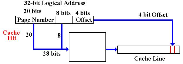
Cache: The Complete Process
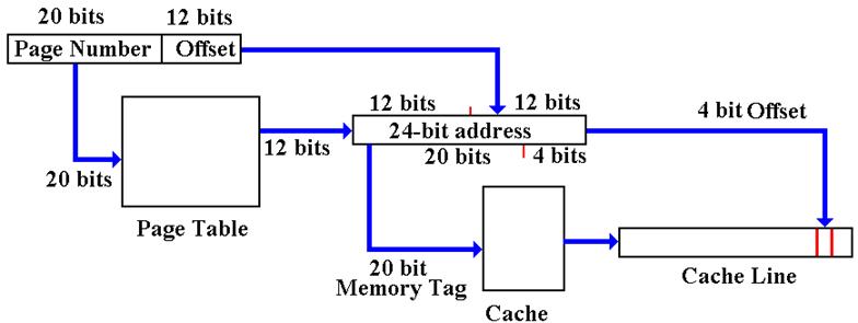
We
start with a 32–bit logical address.
The
virtual memory system uses a page table to produce a 24–bit physical address.
The
cache uses a 24–bit address to find a cache line and produce a 4–bit offset.
This
is a lot of work for a process that is supposed to be fast.
The
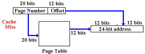
Virtually Mapped Cache
Suppose
that we turn this around, using the high order 28 bits as a virtual tag.
If the addressed item is in the cache, it is found immediately.
A
Cache Miss accesses the Virtual Memory system.
More on
Virtual Memory: Can It Work?
When
there is a cache miss, the addressed item is not in any cache line.
The
virtual memory system must become active.
Is the addressed item in main
memory, or must it be retrieved from the backing store (disk)?
The
page table is accessed. If the page is
present in memory, the page table has the
high–order 12 bits of that page’s physical address.
But wait! The page
table is in memory.
Does this imply
two memory accesses for each memory reference?
This
is where the TLB (Translation Look–aside
Buffer) comes in.
It is a cache for a page table, more accurately called the “Translation Cache”.
The
TLB is usually implemented as a split associative cache.
One associative cache for
instruction pages, and
One associative cache for data
pages.
A
page table entry in main memory is accessed only if the TLB has a miss.
Memory
Segmentation
Memory paging divides the address space into a number of equal
sized blocks,
called pages. The page sizes are fixed for convenience of
addressing.
Memory segmentation divides the program’s address space into logical segments,
into which logically related units are placed.
As examples, we conventionally have
code segments, data segments, stack segments, constant pool segments, etc.
Each
segment has a unique logical name. All accesses to data in a segment must be
through a <name, offset> pair that explicitly
references the segment name.
For
addressing convenience, segments are usually constrained to contain an integral
number of memory pages, so that the more efficient paging can be used.
Memory
segmentation facilitates the use of security techniques for protection.
All
data requiring a given level of protection can be grouped into a single
segment,
with protection flags specific to giving that exact level of protection.
All
code requiring protection can be placed into a code segment and also protected.
It
is not likely that a given segment will contain both code and data. For this reason,
we may have a number of distinct segments with identical protection.