Early Intel Microprocessors
Model Introduced Clock Speed Transistor Count Address Space
4004 11/15/1971 740 kHz 2,300
@ 10 mm 640 bytes
8008 4/1/1972 800 kHz 3,500
@ 10 mm 16 KB
8080 4/1/1974 2 MHz 6,000
@ 6 mm 64 KB
8085 March
1976 5 MHz 6,500
@ 3 mm 64 KB
8086 6/8/1976 10 MHz 29,000
@ 3 mm 1 MB
80286 2/1/1982 25 MHz 134,000 @ 1.5 mm 16 MB
80386 10/17/1985 16 MHz 275,000 @ 1.0 mm 232 bytes
80486 4/10/1989 25 MHz 1.2 million @ 1.0 mm 232 bytes
Pentium 3/22/1993 66 MHz 3.1 million 232 bytes
Pentium 10/10/1994 75 MHz 3.2 million @ 0.6 mm 232 bytes
Pentium 3/27/1995 120 MHz 3.2 million @ 0.6 mm 232 bytes
The 80386 was
the first of the IA–32 family, each of which has a 32–bit
address space, able to address 4GB = 232
bytes.
Legacy of the Intel 8008
The
Intel 4004 was a 4–bit device initially designed to work in a hand–held
calculator that used BCD (4 bit encoded) decimal digits.
The
Intel 8008, as the first of a set of 8–bit designs, was introduced with
no requirement for backward compatibility with the 4004.
The
Intel 8008 had seven general–purpose registers (A, B, C, D, E, H, L),
each of which was an eight–bit register.
We focus on four: A, B, C, and D.
The
introduction of the Intel 8086 in 1976 brought with it the need to expand
these four registers to 16 bits.
The
Intel 80386, introduced in 1983, required 32–bit registers.
How was this to be made compatible with code that required either 8–bit
or 16–bit registers? The answer was a
design trick involving renaming.
The Three Versions of the A Register
The
register renaming conventions will be illustrated for the A register found
in the Intel 8008. It was an 8–bit
register.
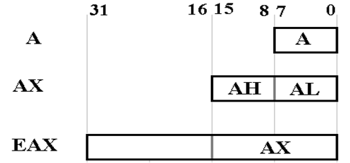
The
Intel 8086 version of the accumulator was called the AX register. It was
split into two halves: the AL and AH, each with 8 bits.
The
Intel 8008 code referencing the A register would now reference the AL.
When the 80386 introduced the use of 32–bit registers, the
accumulator became the
EAX register. It was divided into the AX,
AH, and AL registers, each of which can
be referenced directly by assembly language instructions.
Notes on the IA–32 History
1971 Intel
announces the first microprocessor, its 4004, in November 1971.
This was a four–bit
processor; BCD digits use 4 bits.
1972 An 8–bit
upgrade of the 4004 is announced in April 1972.
It is the 8008.
1974 The Intel
8080 processor is released in April 1974.
It has a 2 MHz clock.
It had 8–bit registers,
and 8–bit data bus, and a 16–bit address bus.
The accumulator was called
the “A register”.
1978 The Intel
8086 and related 8088 processors are released.
Each has 16–bit
registers, 16–bit internal
data busses, and a 20–bit address bus.
Each had
a 5MHz clock; the 8088 ran
at 4.7 MHz for compatibility with the scan rate
of
a standard TV, which could be used as an output device.
The
16–bit accumulator was called the “AX register”. It was divided into two
smaller registers: the AH
register and
According
to Bill Gates “Who would need more than 1 megabyte of memory?”
1980 The Intel
8087 floating–point coprocessor is announced.
Many of the 80x86
series (8088, 8086, 80286,
and 80386) will use a floating–point
coprocessor on a separate
chip.
IA–32 History (Part 2)
1982 The Intel 80286 was announced. It extended the address space to 24 bits,
for an astounding 16
Megabytes allowed. (Intel should have
jumped to
32–bit addressing, but had
convincing financial reasons not to do so).
The
80286 originally had a 6 MHz clock.
A
number of innovations, now considered to be mistakes, were introduced
with the Intel 80286. The first was a set of bizarre memory mapping
options,
which allowed larger
programs to run. These were called “extended memory”
and “expanded memory”. We are
fortunate that these are now history.
Each of
these memory mapping options was based on the use of 64 kB
segments. Unfortunately, it was hard to write code for
data structures that
crossed a segment
boundary, possibly due to being larger than 64 kB.
The
other innovation was a memory protection system, allowing the CPU to
run in one of two modes: real or protected. The only problem
is that no
software developer elected
to make use of these modes.
As a
result of the requirement for backward compatibility, every IA–32
processor since the 80286
must include this mechanism, even if it is not used.
IA–32 History (Part 3)
1983 The
introduction of the Intel 80386, the first of the IA–32 family.
This CPU had 32–bit registers,
32–bit data busses, and a 32–bit address bus.
The 32–bit accumulator was
called the “EAX register”.
The
Intel 80386 was introduced with a 16 MHz clock.
The
80386 had three memory protection modes: protected,
real, and virtual.
We now have three
protection modes that we can ignore.
1989 The
introduction of the Intel 80486, a higher performance version of the
Intel 80386. It originally had a 25 MHz clock. The 80486 DX2, introduced
in 1993, had a 50 MHz
clock.
The
80486 had an 8KB on–chip SRAM cache, used for both instructions and
data. The 80486 DX had an integrated FPU (Floating
Point Unit)
The
80486 was apparently the first Intel CPU to provide the specialized
instructions required to
support multiprocessing. These allow one
processor
to “claim” a memory
location and prevent other processors from accessing
that location until the
value in the location had been updated.
Your
instructor recalls the 80486 as a superior version of the 80386.
IA–32 History (Part 4): The Intel 80586
The Pentium was introduced in March 1993. The design apparently had been named
the Intel 80586 for a short time, but that name was dropped.
The reason for the name change was a dispute over trade
marks. Another company,
AMD (Advanced Micro Devices), had been marketing an 80486.
Before marketing the Pentium, Intel asked to trademark the
name “80586”, but was
told that a number could not be given a trademark. The name was changed to
“Pentium” to prevent AMD from marketing a device with the same name.
AMD did develop and market a chip quite similar to the
Pentium. It was originally
marketed as an 80586, but that name was soon dropped.
In 2000, Intel introduced the Pentium 4 (aka “Pentium IV”),
which represented a
significant redesign of the original Pentium.
By then, clock speeds were 2.0 GHz,
typical of that seen on present–day devices.
In 2001, Intel introduced the Itanium processor. This was the first in the IA–64
series, which supported 64–bit addressing.
Conceptually, this was a radical
redesign of the Pentium, which included a larger general–purpose register set.
However, the IA–64 was still backward compatible. It would run IA–32 code,
and even the old Intel 8008 code.
Supporting Peripheral Devices: Early Decisions
As the CPU designs evolve to support wider data busses and
wider address busses,
this gives rise to the possibility of supporting more sophisticated I/O
devices.
These devices, widely called “peripherals”, might include
hardware such as a printer,
flat–bed scanner, magnetic tape drive, removable disk, and the like.
When the Intel 80386 was introduced, there were three main
design types
in common use.
The Intel 8086, with a 20–bit
address bus and 16–bit data bus.
The Intel 80286, with a 24–bit address bus and 16–bit data
bus.
The Intel 80386, first of the IA–32 line, with 32–bit
address bus and 32–bit data bus.
The compatibility issue was very important in being able to
sell new computers
to customers with installed hardware bases.
The customer might want to use an 8086–compatible device
with a computer
based on the Intel 80286. Could this be
done, when the busses were not compatible?
How about 8086–compatible and 80286–compatible devices with
an Intel 80386?
Backward Compatibility in PC Busses
Here is a figure that shows how the
PC bus grew from a 20–bit address through
a 24–bit address to a 32–bit address while retaining backward compatibility.
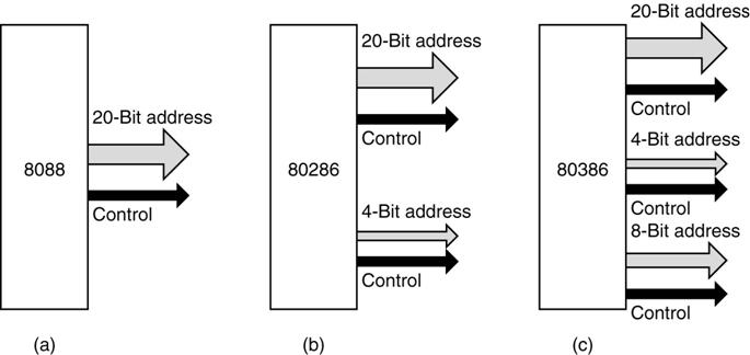
The requirement is that I/O
components (printers, disk drives, etc.) purchased for the
Intel 8088 should be plug–compatible with both the Intel 80286 and Intel 80386.
Those purchased for the Intel 80286
should be plug–compatible with the Intel 80386.
The basic
idea: You are more likely to buy a
new computer if you
can use
your old peripheral devices.
Backward Compatibility in PC Busses (Part 2)
Here is a picture of the PC/AT
(Intel 80286) bus, showing how the original
configuration was kept and augmented, rather than totally revised.
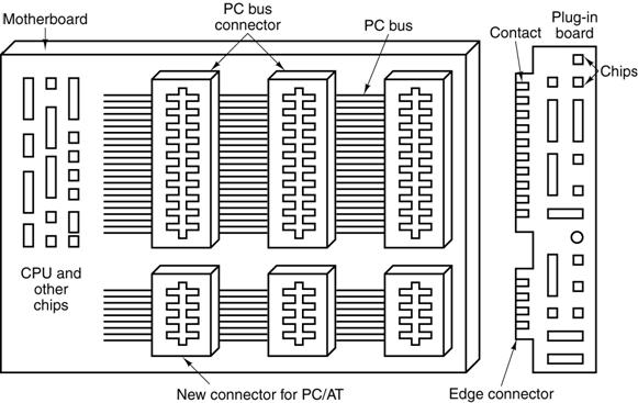
Note that the top slots can be used
by the older 8088 cards, which do not have the
“extra long” edge connectors.
This cannot be used with cards for
the Intel 80386; that would be “forward compatibility”
A Problem with Addressing
Many early computers (including the
PDP–11 manufactured by the Digital Equipment
Corporation, the IBM System/360, and the Intel 8086) faced the problem of
generating
an address that was larger than the number of bits allocated for the address.
Each of the PDP–11 and the Intel
8086 had the same problem and provided the
same solution.
The Intel 8086 was supposed to
support a 20–bit address space, allowing 1MB to
be addressed. However, all address
registers were 16–bit registers.
The answer to this problem, as we
shall soon see, was to use 16–bit segment
registers as well as dedicated address registers.
Each address in this scheme would be
specified by a segment register and an
offset (address) register in the form xxx:yyy, where
xxx denotes the 16–bit value in the segment register ,
and
yyy denotes the 16–bit
value in the offset register.
The IBM System/360 used a similar arrangement with base
registers and offsets.
We discuss that solution in the course on IBM Assembly Language.
Addressing: Segments and Offset
The
Intel 8086 and later use a segmented address system in order to generate
addresses
from 16–bit registers. Each of the main address registers was paired
with an offset.
The IP (Instruction Pointer) register is
paired with the CS (Code Segment)
register.
Each of the IP and CS is a 16–bit register in the earlier designs.
NOTE: The Intel terminology is far superior to the
standard name, the PC (Program
Counter), which is so
named because it does not count anything.
The SP (Stack Pointer) register is paired
with the SS (Stack Segment)
register.
The Intel
8086 used the segment:offset
approach to generating a 20–bit address.
The steps are as follows.
1. The
16–bit value in the segment register is treated as a 20–bit number
with four leading binary
zeroes.
2. This
20 bit value is left shifted by four, shifting out the high order
four 0 bits and shifting
in four low order 0 bits.
3. The
16–bit offset is expanded to a 20–bit number with four leading 0’s
and added to the shifted
segment value. The result is a 20–bit
address.
Example: CS =
0x1234 and IP = 0x2004. 0x12340 +
0x02004 = 0x14344.
The Flat Address Space: Intel 80386 and Later
All
computers in the IA–32 series must support the displacement:offset method of
addressing in order to run legacy code.
This is “backwards compatibility”.
The native
addressing mode in the IA–32 series is called a “flat address space”.
The 16–bit
IP (Instruction Pointer) is now the lower order 16 bits of
the EIP (Extended Instruction Pointer), which can be used without a segment.
The 16–bit
SP (Stack Pointer) is now the lower order 16 bits of
the ESP (Extended Stack Pointer), which also can be used without a segment.
This
diversity of addressing modes has given rise to a variety of “memory models”
based on the addressing needed for code and data.
Memory Models: These are conventional assembly language
models based on the
size of
the code and the size of the data.
Code Size Data Size Model
to Use
Under
64 KB Under 64 KB Small or Tiny
Over 64KB Under 64 KB Medium
Under 64 KB Over 64 KB Compact
Over 64 KB Over 64 KB Large
The smaller memory models give rise to code that is more
compact and efficient.
The IA–32 Register Set
The IA–32
register set contains eight 32–bit registers that might be called
“general purpose”, though they retain some special functions.
These
registers are: EAX, EBX, ECX, EDX, ESP,
EBP, ESI, and EDI.
These are
the 32–bit extensions of the 16–bit registers
AX, BX,
CD, DX, SP, BP, SI, and DI.
The 16–bit
segment registers are: CS, DS, SS, ES, FS and GS.
These appear to be retained only for compatibility with earlier code.
In the
original Intel 8086 design, the AX register was considered as a single
accumulator,
with the other registers assigned supporting roles.
It is
likely that most IA–32 code maintains this distinction, though it is not
required.
Instruction Lengths in the IA–32
It is here
that the IA–32 architecture shows itself to be not RISC.
The IA–32
instruction set originated in the 1970’s when memory was at a premium.
During that time, one have a variety of instruction formats in order to
improve the code density and make better use of memory.
The
instruction lengths commonly supported by the IA–32 architecture are
1 byte, 2 bytes, 3 bytes, 5 bytes, and 6 bytes.
This
variable length considerably complicates the design of an instruction prefetch unit.
The
instruction prefetch unit fetches an instruction
while the previous one
is executing. This trick of fetching and
execution in parallel goes back
at least to the IBM Stretch in the late 1950’s.
Instruction
prefetch in RISC designs, such as the MIPS, is quite
simple.
For most designs, just grab the next four bytes.
For the
IA–32, the number of bytes to be prefetched as the
next instruction
depends on the opcode. This makes for a
more complex and slower control unit.
The IA–64 Architecture
The IA–64
architecture is a design that evolved from the Pentium 4 implementation
of the IA–32 architecture. The basic
issues involve efficient handling of the
complex instruction set that has evolved over the 35 year evolution of the
basic design.
We begin
with a brief discussion of the Pentium 4, introduced in November, 2000.
The Pentium 4 is an implementation of the IA–32 architecture.
The limit
on the clock speed of the Pentium 4 design is set by the power consumption.
The basic issue with power consumption is the heat generated. If the heat is not
removed properly, it can cause the CPU to overheat and malfunction.
The
Pentium 4 is an example of a processor that uses an advanced pipelining scheme,
called “superscalar”, to execute more than one instruction per clock cycle.
The
Pentium 4 converts each binary machine language instruction of the IA–32
Instruction Set Architecture into one or more micro–operations. These are
stored on
the trace cache, which replaces the
Level–1 Instruction Cache.
The IA–64 Architecture (Page 2)
The IA–64
architecture is the outcome of collaboration between Intel and the
Hewlett–Packard Corporation. In some
sense, it is an outgrowth of the Pentium 4.
The IA–64
architecture has many features similar to RISC, but with one major exception:
it expects a sophisticated compiler to issue machine language that can be
exploited
by the superscalar architecture.
The
current implementations of the IA–64 are called the “Itanium” and “Itanium 2”.
One
wonders if the name is based on that of the element Titanium. In any case, the geeks
soon started to call the design the “Itanic”, after
the ship “Titanic”, which sank in 1912.
The
Itanium was released in June 2001: the Itanium 2 in 2002.
Here are some of the features of the IA–64 design.
1. The IA–64 has 128 integer registers and 128
floating–point registers.
2. The IA–64 translates the binary machine
language into 128–bit instruction words
that represent up to three
assembly language instructions that can be executed
during one clock pulse. A sophisticated compile emits these 128–bit
instructions
and is responsible for handling
data and control dependencies. More on this later.
3. The design might be called “VLIW” (Very Long
Instruction Word) except that
Intel seems to prefer “EPIC”
(Explicitly Parallel Instruction Computing).
Intel Hits the Power Wall
The problem is now called “the Power Wall”. It is illustrated in this figure,
taken from Patterson & Hennessy.
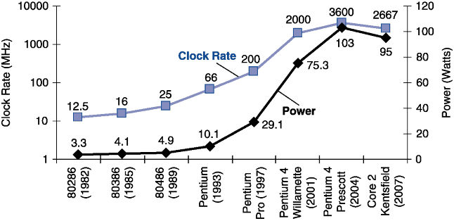
· The design goal for
the late 1990’s and early 2000’s was to drive the clock
rate up. This was done by adding more transistors to a
smaller chip.
· Unfortunately, this
increased the power dissipation of the CPU chip
beyond the capacity of inexpensive
cooling techniques.
The CPU Clock Speed Roadmap (After Some Experience)
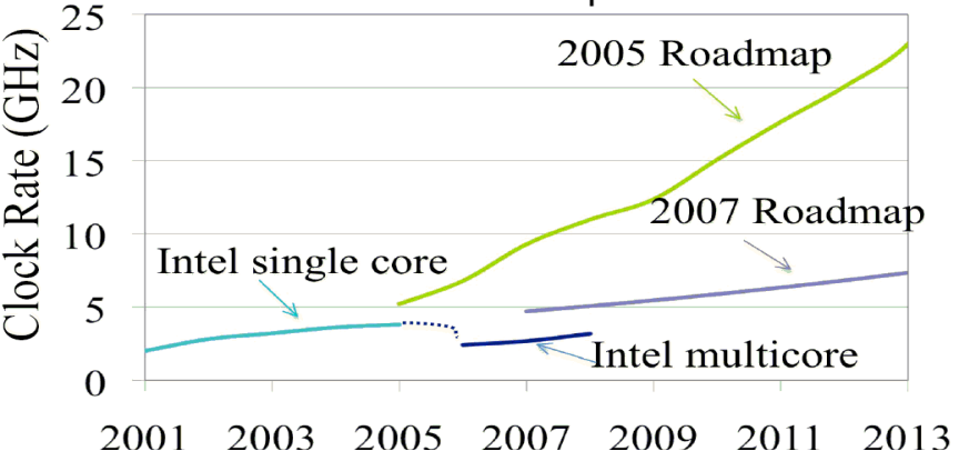
This reflects the practical
experience gained with dense chips that were literally
“hot”; they radiated considerable thermal power and were difficult to cool.
Law of Physics: All electrical power consumed is eventually
radiated as heat.
References
Stanley
Mazor, The History of the Microcomputer – Invention
and Evolution,
Invited Paper in Readings in Computer Architecture, Morgan Kauffman, 2000.
ISBN 1 – 55860 – 539 – 8.
http://en.wikipedia.org/wiki/Intel_80486